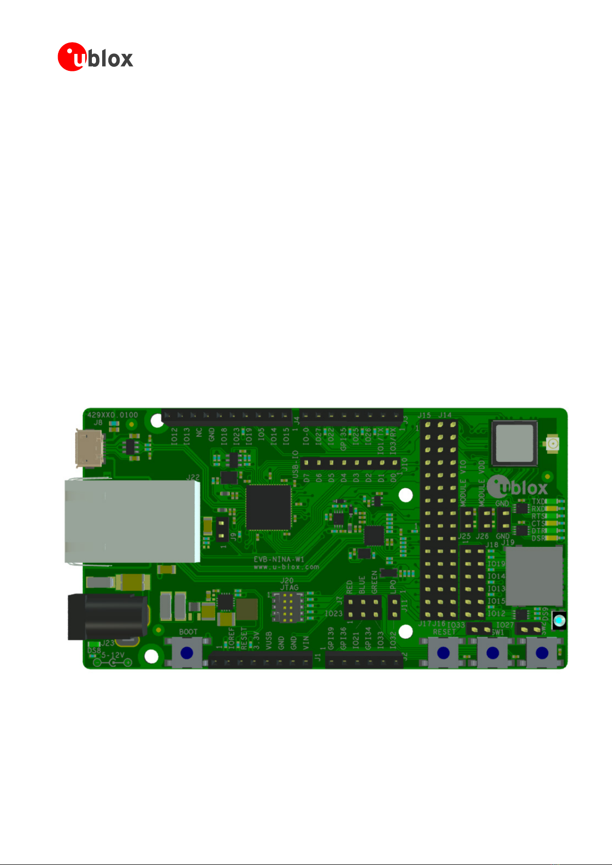
EVK-NINA-W13 - User Guide
UBX-17011007 - R04 Product description
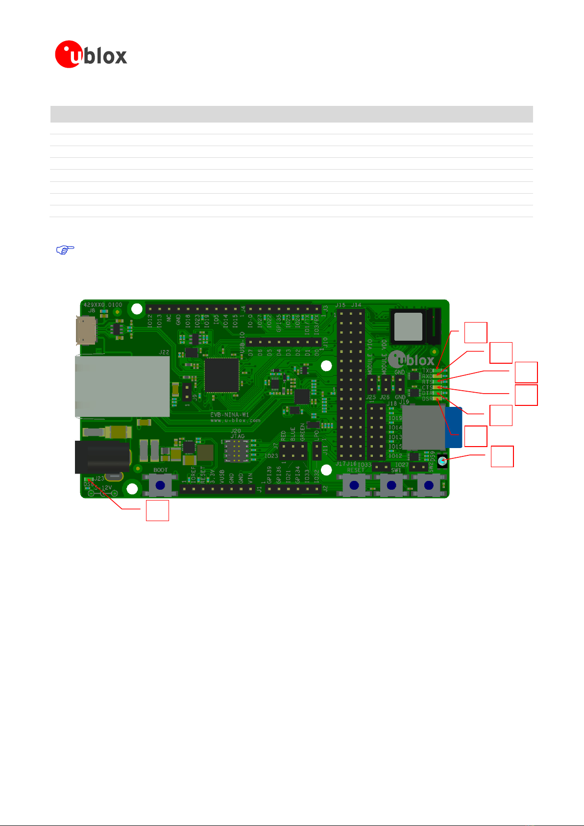
Page 7 of 20
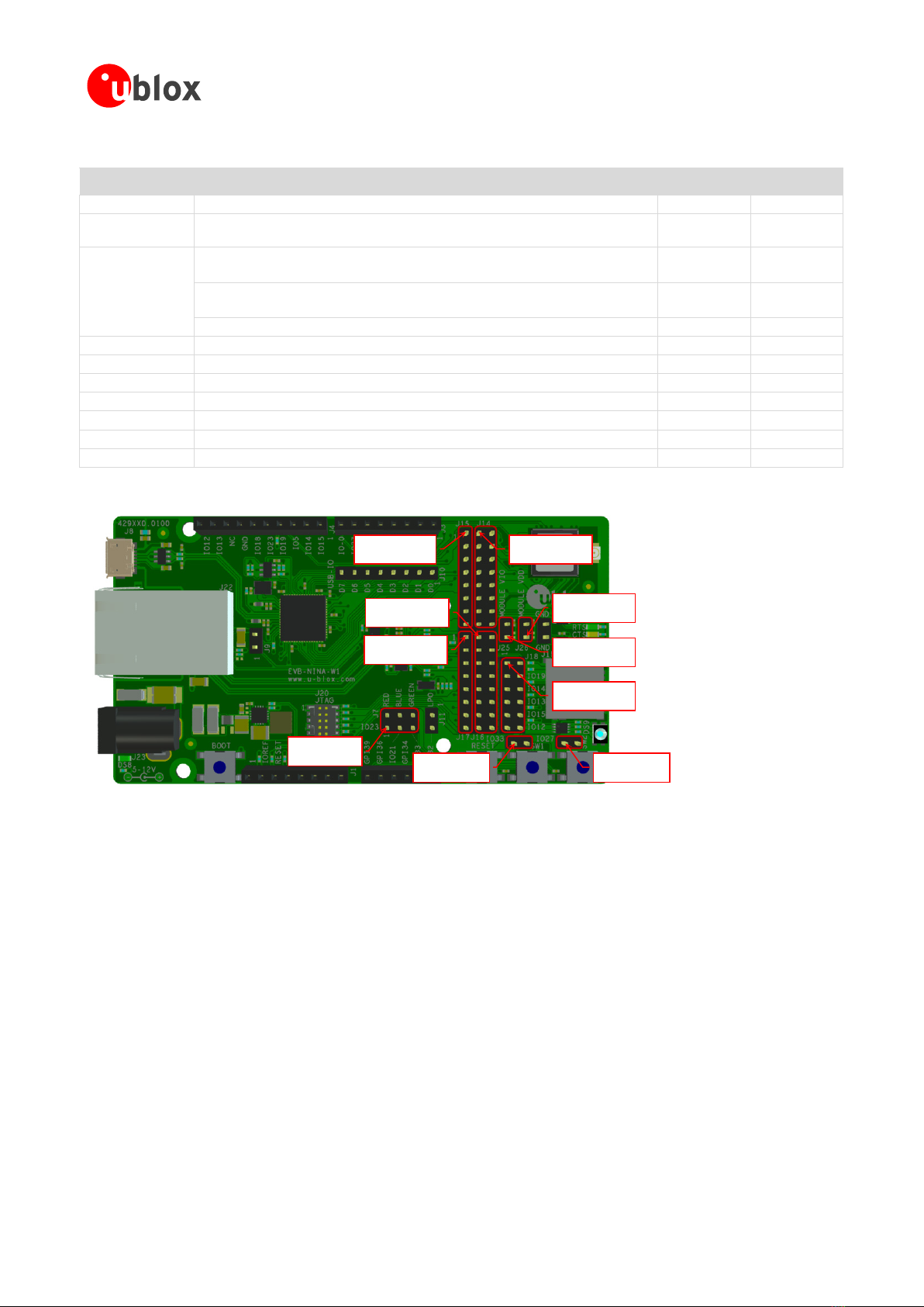
Middle row jumper pin Connected to
J14-1 Module pin-28
J14-3 Module pin-29
J14-5 Module pin-1
J14-7 Module pin-21
J14-9 Module pin-20
J14-11 Module pin-16
J14-13 Module pin-17
J14-15 Module pin-18
J16-1 Module pin-8
J16-3 Module pin-27
J16-5 Module pin-25
J16-7 Module pin-24
J16-9 Module pin-31
J16-11 Module pin-35
J16-13 Module pin-32
J16-15 Module pin-36
Table 2: Available module pins at the middle row of jumpers J14 and J16
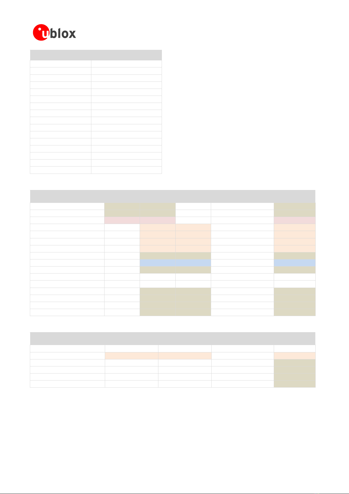
Connected to Left row
jumper pin
Middle row
jumper pin
Right row
jumper pin
Connected to Default
IO-5, J4 pin-3 J15-1 J14-1 J14-2 SPI_CS, U5-PB-3 [ J15-1_J14-1 ]
IO-18, J4 pin-6 J15-2 J14-3 J14-4 SPI_CLK, U5-PB-0 [ J15-2_J14-3 ]
IO-23, J4 pin-5 J15-3 J14-5 J14-6 SPI_MOSI, U5-PB-1 [ J15-3_J14-5 ]
reserved J15-4 J14-7 J14-8 J18 pin-1_3 [ J14-7_J14-8 ]
reserved J15-5 J14-9 J14-10 IO-22, J3 pin-6 (RTS) [ J14-9_J14-10 ]
reserved J15-6 J14-11 J14-12 IO-25, J3 pin-4 (DTR) [ J14-11_J14-12 ]
reserved J15-7 J14-13 J14-14 IO-26, J3 pin-3 (DSR) [ J14-13_J14-14 ]
reserved J15-8 J14-15 J14-16 IO-27, J3 pin-7 [ J14-15_J14-16 ]
reserved J17-1 J16-1 J16-2 IO-21, J2 pin-3 [ J16-1_J16-2 ]
reserved J17-2 J16-3 J16-4 IO-0, J3 pin-8 [ J16-3_J16-4 ]
reserved J17-3 J16-5 J16-6 reserved
reserved J17-4 J16-7 J16-8 reserved
Reserved J17-5 J16-9 J16-10 J18 pin-5 [ J16-9_J16-10 ]
Reserved J17-6 J16-11 J16-12 J18 pin-7 [ J16-11_J16-12 ]
Reserved J17-7 J16-13 J16-14 J18 pin-9 [ J16-13_J16-14 ]
Reserved J17-8 J16-15 J16-16 J18 pin-11 [ J16-15_J16-16 ]
Table 3: IO-allocation via jumpers J14, J15, J16, and J17
Connected to Left row
jumper pin
Right row jumper
pin
Connected to Default
J14-8 J18-1 J18-2 SPI_MISO, U5-PB-2
J14-8 J18-3 J18-4 IO-19, J4 pin-4 (CTS) [ J18-3_J18-4 ]
J16-10 J18-5 J18-6 IO-14, J4 pin-2 [ J18-5_J18-6 ]
J16-12 J18-7 J18-8 IO-13, J4 pin-9 [ J18-7_J18-8 ]
J16-14 J18-9 J18-10 IO-15, J4 pin-1 [ J18-9_J18-10 ]
J16-16 J18-11 J18-12 IO-12, J4 pin-10 [ J18-11_J18-12 ]
Table 4: IO-allocation via jumper J18