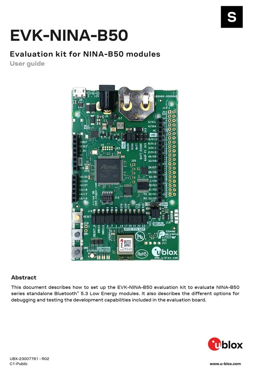
Ublox EVK-NINA-B1 User manual

EVK-NINA-B1
Evaluation kit for NINA-B1 modules
User guide
Abstract
This document describes how to set up the EVK-NINA-B1 evaluation kit to evaluate NINA-B1 series
standalone Bluetooth®Low Energy modules. It also describes the different options for debugging
and the development capabilities included in the evaluation board.
www.u-blox.com
UBX-15028120 - R11

EVK-NINA-B1 - User guide
UBX-15028120 - R11 Page 2 of 21
Document information
Title
EVK-NINA-B1
Subtitle
Evaluation kit for NINA-B1 modules
Document type
User guide
Document number
UBX-15028120
Revision and date
R11
21-Oct-2019
Disclosure restriction
This document applies to the following products:
Product name
Type number
Firmware version
PCN reference
EVK-NINA-B111
EVK-NINA-B111-00
EVK-NINA-B112
EVK-NINA-B112-00
u-blox or third parties may hold intellectual property rights in the products, names, logos and designs included in this
document. Copying, reproduction, modification or disclosure to third parties of this document or any part thereof is only
permitted with the express written permission of u-blox.
The information contained herein is provided “as is” and u-blox assumes no liability for its use. No warranty, either express or
implied, is given, including but not limited to, with respect to the accuracy, correctness, reliability and fitness for a particular
purpose of the information. This document may be revised by u-blox at any time without notice. For the most recent
documents, visit www.u-blox.com.
Copyright © u-blox AG.

EVK-NINA-B1 - User guide
UBX-15028120 - R11 Page 3 of 21
Contents
Document information................................................................................................................................2
Contents ..........................................................................................................................................................3
1Product description ..............................................................................................................................4
1.1 Overview........................................................................................................................................................4
1.2 Kit includes ................................................................................................................................................... 5
1.3 Jumper description ....................................................................................................................................5
1.4 LEDs...............................................................................................................................................................5
1.5 Connectors ................................................................................................................................................... 6
1.6 Buttons..........................................................................................................................................................9
1.7 Configuration options ................................................................................................................................9
1.7.1 Power supply........................................................................................................................................9
1.7.2 Disconnecting the debug MCU interface and LEDs ..................................................................10
1.7.3 NFC antenna interface ....................................................................................................................11
1.7.4 Current measurement .....................................................................................................................11
1.8 Software debug options ..........................................................................................................................12
2Setting up the evaluation board ..................................................................................................... 13
2.1 Evaluation board setup............................................................................................................................13
2.2 Starting up .................................................................................................................................................13
2.3 Getting the latest software ....................................................................................................................13
Appendix ........................................................................................................................................................ 14
BGlossary .................................................................................................................................................. 19
Related documents ................................................................................................................................... 20
Revision history.......................................................................................................................................... 20
Contact........................................................................................................................................................... 21

EVK-NINA-B1 - User guide
UBX-15028120 - R11 Product description Page 4 of 21
1Product description
1.1 Overview
The EVK-NINA-B1 evaluation kit includes an evaluation board, which can be used as a reference
design for the NINA-B1 series modules, a quick start guide, an NFC antenna, and a USB cable. For the
NINA-B111 module, the evaluation board has a U.FL coaxial connector for connecting to the external
antenna. The NINA-B112 module has an onboard antenna; thus the evaluation board does not have a
U.FL connector.
The main features of the EVK-NINA-B1 are:
Available in two variants - NINA-B111 and NINA-B112
All the NINA-B1 module pins are available at connectors
Can be powered through USB, external power supply, or coin cell battery
Has an onboard debug MCU that allows serial communication and flashing/debugging over USB.
The EVK-NINA-B1 evaluation kits are available in the following two different versions depending on
the NINA-B1 series module that is mounted:
EVK-NINA-B111 –Evaluation kit for NINA-B111module with antenna pin
EVK-NINA-B112 –Evaluation kit for NINA-B112 module with onboard antenna
This section describes the main connectors and settings that are required to get started. Figure 1
shows the EVK-NINA-B1 evaluation board.
Figure 1: EVK-NINA-B1 evaluation board
⚠Take care when handling the EVK-NINA-B112. Applying force to the NINA-B112 module might
damage the internal antenna.

EVK-NINA-B1 - User guide
UBX-15028120 - R11 Product description Page 5 of 21
1.2 Kit includes
The EVK-NINA-B1 evaluation kit includes the following:
NINA-B1 evaluation board
2.4 GHz antenna with u.fl connector (only in EVK-NINA-B111)
NFC antenna
USB cable
Quick Start card
1.3 Jumper description
Parameter
Description
Name
Default
Power source
selector
Selects the source from where the board is powered
J7
External/USB
Peripheral
connections
Selects the signals that will be connected to the
module peripherals such as LEDs and MCU
interface
J9
All mounted
Table 1: EVK-NINA-B1 jumper description
1.4 LEDs
Function
Description
Name
Color
Orange Debugger
LED
Red when EVK (both module and debug chip) is in reset
DS5
Orange
Green Debugger LED
Non blinking LED shows comunication link between the
debug chip and the PC.
DS6
Green
UART Rx
Blinking LED shows UART Rx activity
DS7
Green
UART Tx
Blinking LED shows UART Tx acitivty
DS8
Orange
UART CTS
Blinking LED shows CTS activity
DS1
Green
UART RTS
Blinking LED shows RTS activity
DS2
Orange
RGB LED
RGB LED shows status for
u-connectXpress
☞See the NINA-B1 data sheet [1] for additional
information.
DS9
RGB
Table 2: EVK-NINA-B1 LEDs description

EVK-NINA-B1 - User guide
UBX-15028120 - R11 Product description Page 7 of 21
Figure 3: EVK-NINA-B1 connectors
Connector
Description
J1, J2, J3, J4 and J18
Connectors for accessing all GPIOs on NINA-B1
J12
Serial wire debug connector for NINA-B1 module
J10
U.FL connector for external antenna (EVK-NINA-B111 only)
J11
Pin header for NFC antenna connection
J5
Power jack
BT1
Battery holder
J8
USB connector
J15
Module VCC power rail header
J6
Module VCC_IO power rail header
J17
External 5-12V supply pin
Table 3: EVK-NINA-B1 connector description
Conn.
NINA-B1
Pin No.
nRF52
pin
Arduino
pin
Description
Schematic
net name
Alternate functions and notes
J1
1
-
N/C
Not Connected
-
Not connected
2
-
IOREF
I/O reference voltage level.
Selectable by user to 1.7 –3.6 V
VDD_IO
See section 1.7.1
3
P0.21
RESET
Reset signal input. Active low logic
RESET_N
4
-
3.3V
3.3 V DC regulated supply output
3V3

EVK-NINA-B1 - User guide
UBX-15028120 - R11 Product description Page 8 of 21
Conn.
NINA-B1
Pin No.
nRF52
pin
Arduino
pin
Description
Schematic
net name
Alternate functions and notes
5
-
5V
5 V regulated supply output
5V
Cannot be used as supply input, use
VIN instead. Only supplied by USB
VBUS.
6
GND
GND
Ground
GND
7
GND
GND
Ground
GND
8
-
VIN
External DC supply input, 5 –12 VDC
VIN
J2
1
P0.03
A0
Analog input
GPIO_25
Analog function capable GPIO
2
P0.02
A1
Analog input
GPIO_24
Analog function capable GPIO
3
P0.04
A2
Analog input
GPIO_27
Analog function capable GPIO
4
P0.30
A3
Analog input
SWITCH_2/
GPIO_18
Analog function capable GPIO,
SWITCH_2 on NINA-B1.
This signal is pulled low when the
button SW2 is pressed
5
P0.29
A4
Analog input
UART_DSR/
GPIO_17
Analog function capable GPIO,
UART_DSR signal on NINA-B1
6
P0.28
A5
Analog input
UART_DTR/
GPIO_16
Analog function capable GPIO,
UART_DTR signal on NINA-B1
J3
1
P0.05
D0/RX
Digital I/O, UART RX
UART_RXD/
GPIO_23
UART_RXD signal on NINA-B1
2
P0.06
D1/TX
Digital I/O, UART TX
UART_TXD/
GPIO_22
UART_TXD signal on NINA-B1
3
P0.07
D2
Digital I/O
UART_CTS/
GPIO_21
UART_CTS signal on NINA-B1
4
P0.31
D3
Digital I/O
UART_RTS/
GPIO_20
UART_RTS signal on NINA-B1
5
P0.18
D4
Digital I/O
GPIO_8
SWO signal on NINA-B1
6
-
D5
Digital I/O
GPIO_15
SWDIO
7
P0.09
D6
Digital I/O
GPIO_28
Configured for NFC use
8
P0.10
D7
Digital I/O
GPIO_29
Configured for NFC use
J4
1
-
D8
Digital I/O
GPIO_11
SWDCLK
2
P0.08
D9
Digital I/O
GPIO_1
3
P0.11
D10
Digital I/O
GPIO_2
4
P0.13
D11
Digital I/O
GPIO_4
5
P0.12
D12
Digital I/O
GPIO_3
6
P0.14
D13
Digital I/O
GPIO_5
7
GND
Ground
GND
8
-
AREF
Analog reference voltage level
-
Not connected
9
P0.02
SDA
I2C data signal
GPIO_24
10
P0.03
SCL
I2C clock signal
GPIO_25
Table 4: Pin number mapping of NINA-B1 Module and nRF52
☞The EVK-NINA-B1 has an I/O voltage range of 1.7-3.6 V. It can therefore be used only with
shields that support an I/O voltage within this range.
The EVK-NINA-B1 has a pinout that is compatible with some Arduino or Arduino inspired shields. This
section describes the features of the EVK pins that a shield has to comply with:
IOREF: The I/O voltage level of the NINA-B1 module. Is 3.3 V by default, but the EVK can be modified
to allow for other voltages (1.7-3.6 V).
RESET: Is connected to the RESET button (SW0).

EVK-NINA-B1 - User guide
UBX-15028120 - R11 Product description Page 9 of 21
3.3 V: A regulated 3.3 V output or the battery supply voltage, depending on the power configuration
used. May only be used as a 3.3 V input if no jumpers are mounted on jumper J7.
5 V: Is only a 5 V supply output if the EVK is being powered by USB. If any other power configuration
is used, this pin will be unconnected (floating). It is safe to connect an external 5 V supply to this
pin when the USB power configuration is not used.
VIN: May be used as a 3.8-12 V supply input to power the EVK-NINA-B1.
A0: Is also connected to the EVK pin SCL (NINA pin 25).
A1: Is also connected to the EVK pin SDA (NINA pin 24).
Pin 0 (RX): Is connected to the NINA-B1 UART RX pin (NINA pin 23).
Pin 1 (TX): Is connected to the NINA-B1 UART TX pin (NINA pin 22).
SDA: Is also connected to the EVK pin A1.
SCL: Is also connected to the EVK pin A0.
☞Note on SCL/SDA: On some Arduino boards, the I2C signals, SCL and SDA, are connected to
the pins A4 and A5 while on some other boards, it is connected to the SCL and SDA pins in the
top right hand corner. Some shields therefore short these pins together. This can cause
problems when using the EVK-NINA-B1 as in this scenario, the SCL/SDA pins are also
connected to the A0/A1 pins.
☞Note on digital I/O pins: Some of the digital I/O pins can be connected to the
on-board debug MCU, thus allowing serial communication and flashing/debugging over USB.
This can cause interference on signals that are also used by an Arduino shield. See Section
1.7.2 on how to disconnect these signals from the debug MCU.
1.6 Buttons
The EVK-NINA-B1 evaluation board has four buttons. Three of them are directly connected to NINA-
B1 pins. The fourth button is connected to the debug MCU interface.
Button
Description
SW0
NINA-B1 reset button connected to pin 19
SW1
General function button connected to pin 7
SW2
General function button connected to pin 18
Table 5: EVK-NINA-B1 buttons description
1.7 Configuration options
1.7.1 Power supply
The EVK-NINA-B1 can be powered the following different ways:
USB
External power supply
CR2032 coin cell battery
Depending on the selected power source, and whether or not NFC will be used, you must fit the jumper
on pin header J7 in one of the three different positions as shown in Figure 4.

EVK-NINA-B1 - User guide
UBX-15028120 - R11 Product description Page 10 of 21
Figure 4: Power supply jumper positions of EVK-NINA-B1
1. To power the board from USB or external power supply, the jumper on J7 should be in position
1 as shown in Figure 4.
2. To power the board from the CR2032 coin cell battery for applications where NFC is not used,
the jumper on J7 should be in position 2.
3. To power the board from the CR2032 coin cell battery for applications where NFC will be used,
the jumper on J7 should be in position 3. The rationale for this is that the high field strength
on the NFC antenna can cause reverse current flow to the coin cell battery –hence the
possibility to connect the D4 diode as a protection for the reverse current.
If you would like to utilize the flexible input voltage 1.7-3.6 V of the NINA-B1 module, the power source
has to be connected to header J7. Connect the positive voltage to one of the pins - 1, 2 or 3 (bottom
row in Figure 4) and connect the ground to one of the two pins marked “GND” in Figure 4.
Coin cell battery considerations
When powering the EVK with a coin cell battery, keep in mind that the debug MCU will also have to be
powered by the battery. This will drain the battery faster than needed for a realistic solution. The
debug chip can be disabled to minimize the leakage during a battery powered setup. This is done by
removing resistor R9; R9 is shown in Figure 5.
Figure 5: Resistor R9
1.7.2 Disconnecting the debug MCU interface and LEDs
The J9 pin header includes all signals that are passed between the NINA-B1 module, the MCU
interface, and the LEDs.
If for some reason, you do not need these connections, then there is a possibility to disconnect these
signals separately by removing the selected jumpers. For instance, this could be useful in a current
measurement scenario.

EVK-NINA-B1 - User guide
UBX-15028120 - R11 Product description Page 11 of 21
Figure 6: Peripherals connection pin header of EVK-NINA-B1
1.7.3 NFC antenna interface
The NFC antenna interface is available on the J11 connector. The default configuration is shown in
Figure 7. 0 Ωresistors are mounted on R15 and R16. This connects the J11 NFC antenna connector
to pins 28 and 29 of the NINA-B1 module. If NFC is not needed, and pins 28 and 29 are used as GPIOs
available on connector J3, then resistors on R15 and R16 should be removed and instead mounted on
R13 and R14.
Figure 7: NFC antenna interface J11 of EVK-NINA-B1
1.7.4 Current measurement
The EVK-NINA-B1 offers the possibility to measure current consumption for the NINA-B1 module.
Figure 8: Current measurement pin header J15 of EVK-NINA-B1
The current consumption for the NINA-B1 module on the EVK-NINA-B1 can be measured in two ways
as explained in the following subsections.

EVK-NINA-B1 - User guide
UBX-15028120 - R11 Product description Page 12 of 21
Figure 9: Placement of R4 and R6 (10 Ωresistors)
1.7.4.1 Current measurement with ampere-meter
Remove the jumpers on J15 and J6. Remove the 10 Ωresistors R4 and R6 and connect the ampere-
meter in series between the pins 1 and 2 of the J15 pin header. This will give the NINA-B1 current
consumption reading on the ampere-meter.
1.7.4.2 Current measurement with Oscilloscope
Remove the 10 Ωresistor on R4. Remove the jumpers on J15 and J6 and connect an oscilloscope to
pins 1 and 2 of the J15 pin header. Then, this will display the voltage drop over the R6 resistor. Current
consumption will be proportional to the voltage drop.
If R6=1 Ω, then 1 mV voltage drop equals 1 mA of current. If R6=10 Ω, then 10 mV voltage drop equals
1 mA of current.
⚠The USB interface, MCU interface, and the LEDs should not be connected during current
consumption measurement.
1.8 Software debug options
You can debug the software using the following two options in EVK-NINA-B1:
Onboard debug solution available on the USB connector
Using an external debugger connected to J12 connector
An external debugger connected to the J12 connector is useful when powering the evaluation board
with the CR2032 coin cell battery, or through the external power supply connector J5. It could also be
useful in a scenario where the debug MCU interface has been disconnected from the NINA-B1 module
using the jumpers on J9 header. The SEGGER J-Link software [5] is required to debug using the
onboard J-Link hardware on the EVK-NINA-B1.

EVK-NINA-B1 - User guide
UBX-15028120 - R11 Setting up the evaluation board Page 13 of 21
2Setting up the evaluation board
2.1 Evaluation board setup
The EVK-NINA-B1 will be delivered with the u-blox Connectivity Software installed on the module.
Before connecting the module, download and install the latest u-blox s-center evaluation software
from the u-blox website.
To use Bluetooth Low Energy on the EVK-NINA-B111, connect a 2.4 GHz antenna to the U.FL antenna
connector (J10). The EVK-NINA-B112 has an onboard antenna.
Plug in either an external power supply in J5 connector or connect to a USB host with a USB cable
attached to J8 connector. You can also power the evaluation board with a CR2032 coin cell battery.
The status light (DS6) will turn green, indicating it has power. The NFC antenna can be connected to
the J11 connector.
⚠Be careful to check polarity before connecting external power supply to the EVK-NINA-B1
evaluation board. Center conductor is positive (+) and the ring is negative (-).
The operating system will install the correct drivers automatically. The drivers will only need to be
installed the first time you connect the unit to a new computer.
⚠If the drivers are not installed automatically, download the nRFgo Studio from
www.nordicsemi.com to get the Jlink CDC UART driver.
A COM port will automatically be assigned to the unit by Windows. On Windows 7, open the Control
Panel, click Hardware and Sound. Click Device Manager in Devices and Printers. This will open Device
Manager window where you can view the assigned COM ports.
2.2 Starting up
Perform the following steps to enable communication with the module:
1. Start the u-blox s-center evaluation software.
2. Use the default baudrate 115200, 8N1 with flow control.
3. You will now be able to communicate with the module through AT-commands.
For a list of available AT commands, see the u-blox Short Range AT Commands Manual [3].
To get started with basic use case setups of the EVK-NINA-B1 with u-blox Connectivity Software, see
the NINA-B1 Getting Started [3].
If you would like to use the EVK-NINA-B1 together with Nordic Semiconductor SDK or Arm®MbedTM
operating system, refer to the Software section of the NINA-B1 System Integration Manual [2].
2.3 Getting the latest software
Go to the u-blox support webpage to obtain the latest available firmware. Instructions on reflashing
the EVK-NINA-B1 can be found in the Software section of the NINA-B1 System Integration Manual
[2].

EVK-NINA-B1 - User guide
UBX-15028120 - R11 Appendix Page 14 of 21
Appendix
ASchematics

EVK-NINA-B1 - User guide
UBX-15028120 - R11 Appendix Page 15 of 21

EVK-NINA-B1 - User guide
UBX-15028120 - R11 Appendix Page 16 of 21

EVK-NINA-B1 - User guide
UBX-15028120 - R11 Appendix Page 17 of 21

EVK-NINA-B1 - User guide
UBX-15028120 - R11 Appendix Page 18 of 21

EVK-NINA-B1 - User guide
UBX-15028120 - R11 Appendix Page 19 of 21
B Glossary
Abbreviation
Definition
API
Application programming Interface
CTS
Clear To send
EVK
Evaluation kit
GND
Ground
GPIO
General-Purpose Input/Output
LED
Light-Emitting Diode
MCU
Micro controller unit
MSD
Mass storage device
NFC
Near Field Communication
U.FL
Coaxial RF connector
USB
Universal serial bus
RTS
Request to send
SDK
Software development kit
SPA
Serial port application
UART
Universal Asynchronous Receiver/Transmitter
Table 6: Explanation of the abbreviations and terms used

EVK-NINA-B1 - User guide
UBX-15028120 - R11 Related documents Page 20 of 21
Related documents
[1] NINA-B1 data sheet, doc. no. UBX-15019243
[2] NINA-B1 series system integration manual, doc. no. UBX-15026175
[3] u-blox Short range AT commands manual, doc. no. UBX-14044127
[4] NINA-B1 getting started doc. no. UBX-16009942
[5] SEGGER J-Link software - https://www.segger.com/jlink-software.html
☞For regular updates to u-blox documentation and to receive product change notifications,
register on our homepage (www.u-blox.com).
Revision history
Revision
Date
Name
Comments
R01
22-Feb-2016
phak,fbro,
kgom
Initial release.
R02
26-May-2016
fbro
Updated information about current measurement (section 1.7.4). Updated
the links to Nordic resources in section 2.2. Removed SW3 from section 1.6.
R03
17-Jun-2016
fbro, kgom
Modified the document status to Advance Information. Modified Figure 3 and
Table 3. Included information about the u-blox NINA-B1 firmware (section 2).
R04
5-Jul-2016
fbro, kgom
Included information about how to flash the EVK-NINA-B1.
R05
9-Sep-2016
fbro, kgom
Modified Figure 2. Updated the section “UART flashing”. Changed the
document status to Early Production Information.
R06
24-Oct-2016
apet, kgom
Added information about mbed OS.
R07
1-Mar-2017
ajoh, fbro,
kgom, apet
Included information on Arduino shield compatibility. Added schematics and
placement (Appendix A). Updated all the figures. Replaced Document status
with Disclosure restriction.
R08
16-May-2017
kgom
Minor updates.
R09
23-Nov-2017
kgom
Minor changes based on the recent brand guidelines of Arm Mbed.
R10
6-Dec-2018
mwej, fbro,
kgom
Added a new table describing Arduino to NINA to nRF pin numbering
(Table 4).
R11
21-Octa-2019
flun
Clarified the status for RGB LED in Table 2 (section 1.4).
This manual suits for next models
4
Table of contents
Other Ublox Motherboard manuals

Ublox
Ublox C030-R412M User manual

Ublox
Ublox EVK-L20 User manual

Ublox
Ublox EVK-JODY-W3 User manual

Ublox
Ublox C099-F9P User manual

Ublox
Ublox EVK-M101 User manual

Ublox
Ublox BMD-34 Series User manual

Ublox
Ublox EVK-R6 User manual

Ublox
Ublox EVK-N2 Series User manual

Ublox
Ublox EVK-M9DR User manual

Ublox
Ublox EVK-BMD-340 User manual

Ublox
Ublox SARA-R5 Series User manual

Ublox
Ublox EVK-M10QSAM User manual

Ublox
Ublox EVK-NORA-W36 User manual

Ublox
Ublox EVK-R6 User manual

Ublox
Ublox EVK-NORA-B1 User manual

Ublox
Ublox EVK-U2X User manual

Ublox
Ublox EVK-NINA-B3 Series User manual

Ublox
Ublox EVK-JODY-W2 User manual

Ublox
Ublox C102-F9R User manual

Ublox
Ublox EVK-M8L User manual