Ublox EVK-VERA-P174 User manual

EVK-VERA-P174
Evaluation kit for VERA-P1 Host-based V2X transceiver
modules
User Guide
Abstract
This document describes how to set up the EVK-VERA-P174 evaluation kit to evaluate the VERA-P1
series host-based 802.11p V2X transceiver modules.
www.u-blox.com
UBX-17048707 - R06

EVK-VERA-P174 - User Guide
UBX-17048707 - R06 Page 2 of 30
Document Information
Title
EVK-VERA-P174
Subtitle
Evaluation kit for VERA-P1 Host-based V2X transceiver modules
Document type
User Guide
Document number
UBX-17048707
Revision and date
R06
17-Apr-2019
Disclosure Restriction
This document applies to the following products:
Product name
Type number
Firmware version
PCN reference
EVK-VERA-P174
EVK-VERA-P174-00A-00
N/A
u-blox or third parties may hold intellectual property rights in the products, names, logos and designs included in this
document. Copying, reproduction, modification or disclosure to third parties of this document or any part thereof is only
permitted with the express written permission of u-blox.
The information contained herein is provided “as is” and u-blox assumes no liability for its use. No warranty, either express or
implied, is given, including but not limited to, with respect to the accuracy, correctness, reliability and fitness for a particular
purpose of the information. This document may be revised by u-blox at any time without notice. For the most recent
documents, visit www.u-blox.com.
Copyright © u-blox AG.

EVK-VERA-P174 - User Guide
UBX-17048707 - R06 Page 3 of 30
Contents
Document Information................................................................................................................................ 2
Contents ..........................................................................................................................................................3
1Evaluation kit description...................................................................................................................5
1.1 Overview........................................................................................................................................................5
1.2 Kit includes ................................................................................................................................................... 6
1.3 Software and documentation...................................................................................................................6
1.4 System requirements ................................................................................................................................6
1.5 Specifications .............................................................................................................................................. 7
2Getting started.......................................................................................................................................8
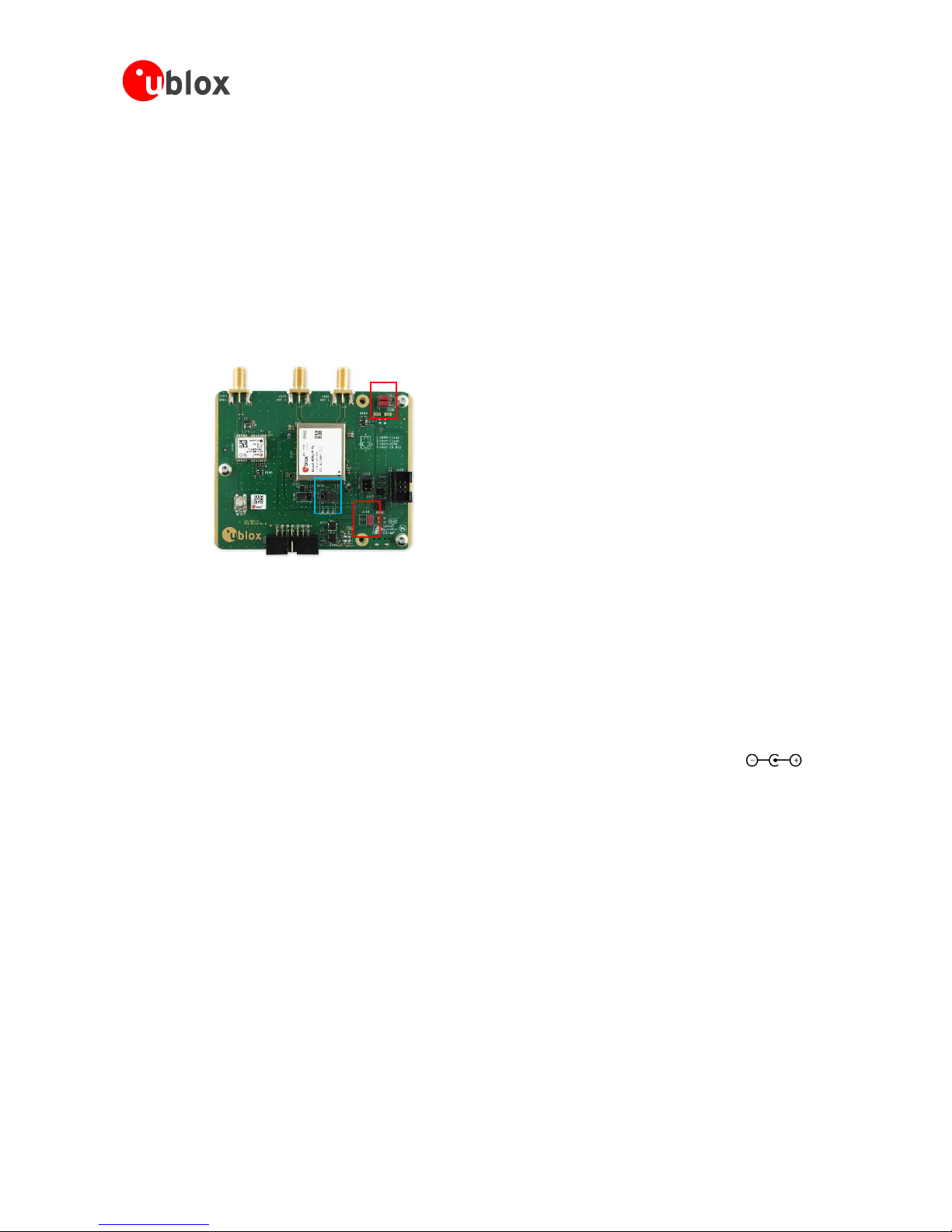
3Board description...................................................................................................................................9
3.1 Block diagram .............................................................................................................................................. 9
3.2 Overview........................................................................................................................................................9
3.2.1 Main board .........................................................................................................................................10
3.2.2 USB and power supply board..........................................................................................................10
3.3 Connectors .................................................................................................................................................12
3.3.1 Power supply and configuration ....................................................................................................12
3.3.2 USB interface.....................................................................................................................................12
3.3.3 Bootstrapping....................................................................................................................................12
3.3.4 SPI interface ......................................................................................................................................12
3.3.5 SPI chip select ...................................................................................................................................13
3.3.6 1PPS interface...................................................................................................................................13
3.3.7 GNSS interface..................................................................................................................................13
3.3.8 SMA connectors................................................................................................................................14
3.3.9 Host interface connector ................................................................................................................14
3.4 LEDs.............................................................................................................................................................14
3.5 Buttons........................................................................................................................................................14
3.6 Design files .................................................................................................................................................14
4Software ................................................................................................................................................ 20
4.1 Quick start instructions...........................................................................................................................20
4.2 Module calibration ....................................................................................................................................22
4.3 Usage examples ........................................................................................................................................23
4.3.1 Transmit and receive counters ......................................................................................................23
4.3.2 Channel configuration .....................................................................................................................24
4.3.3 Transmitter test ...............................................................................................................................24
4.3.4 Receiver test ......................................................................................................................................25
4.3.5 LLC native IPv6 functionality .........................................................................................................26
4.4 Building the software for a different target platform .......................................................................27
Appendix ....................................................................................................................................................... 28
AGlossary ................................................................................................................................................. 28
Related documents ....................................................................................................................................29

EVK-VERA-P174 - User Guide
UBX-17048707 - R06 Page 4 of 30
Revision history...........................................................................................................................................29
Contact.......................................................................................................................................................... 30

EVK-VERA-P174 - User Guide
UBX-17048707 - R06 Evaluation kit description
Page 5 of 30
1Evaluation kit description
1.1 Overview
VERA-P1 is a compact, embedded transceiver module that enables development of electronics for
Vehicle-to-Everything (V2X) communication systems. The module includes an integrated
MAC/LLC/Baseband processor and the required RF front-end components. It connects to a host
processor through USB or SPI interface.
The EVK-VERA-P174 evaluation kit provides a simple way to evaluate the VERA-P1 series host-
based V2X transceiver modules. The evaluation kit serves as an evaluation and development
platform providing full access to the interfaces of the VERA-P1 radio module, and allows integration
of the VERA-P1 module with an external PC or host processor development platform.
The main features of the EVK-VERA-P174 evaluation kit are:
Enables host communication via Micro USB connector or SPI pin header
Provides two SMA antenna connectors for the VERA-P1 module
Has an integrated u-blox NEO-M8U GNSS module with SMA antenna connector
Has an on-board SPI flash for evaluating different boot options
Provides an integrated USB 2.0 hub to access VERA-P1, GNSS, and SPI flash via a single
connector
Has 9 –28 V DC power supply input with the option to provide external supplies separately and
measure current consumption
Table 1 lists the available versions of the evaluation kit:
Evaluation kit
Description
Suitable for evaluation of
EVK-VERA-P174
Evaluation kit for the VERA-P1 module
VERA-P173 (with single radio firmware)
VERA-P174 (with dual radio firmware)
Table 1: EVK-VERA-P174 evaluation kit
☞See the VERA-P1 series Data Sheet [1] and VERA-P1 series System Integration Manual [2] for
the features supported by VERA-P1 series V2X modules.
The EVK-VERA-P174 consists of two boards, which are connected by a board-to-board connector.
The upper main board contains the VERA-P174 and the NEO-M8U GNSS module. The USB interface
and main power supply are included on the lower power supply board. The board-to-board connector
allows the main board to be directly connected to a compatible host board.

EVK-VERA-P174 - User Guide
UBX-17048707 - R06 Evaluation kit description
Page 6 of 30
Figure 1: EVK-VERA-P174 main board
1.2 Kit includes
The EVK-VERA-P174 evaluation kit includes the following:
Evaluation board with the VERA-P174 module (main and power supply boards)
Two 5.9 GHz DSRC antennas (Triton TD.10 5 dBi)
Micro USB cable
Quick Start card
1.3 Software and documentation
The Linux drivers, firmware, and basic evaluation tools for the VERA-P1 series modules are available
via u-blox support. Distribution of the software requires signing of the u-blox Limited Use License
Agreement (LULA-N).
☞Contact u-blox support for your area as listed in the Contact section to obtain the software
package.
1.4 System requirements
Host PC with a USB 2.0 interface
Native Linux OS or virtual machine for building and running the software (for example, Ubuntu
18.04)

EVK-VERA-P174 - User Guide
UBX-17048707 - R06 Evaluation kit description
Page 7 of 30
1.5 Specifications
Table 2 and Table 3 list the absolute maximum ratings and operating conditions for the
EVK-VERA-P174:
Symbol
Description
Min.
Max.
Unit
V_Sys
Main power supply 9 –28 V
-0.3
28.0
V
5V0_A1,
5V0_A2
Power supply voltage 5 V
-0.3
6.0
V
3V3
Power supply voltage 3.3 V
-0.3
3.9
V
VIO
I/O supply voltage 1.8 V/3.3 V
-0.3
3.9
V
TSTORAGE
Storage temperature
-40
+95
ºC
Table 2: Absolute maximum ratings
Symbol
Description
Min.
Typ
Max.
Unit
V_Sys
Main power supply voltage
9
12
28
V
5V0_A1,
5V0_A2
Power supply voltage 5.0 V
4.5
5.0
5.5
V
3V3
Power supply voltage 3.3 V
3.0
3.3
3.6
V
VIO
I/O supply voltage 1.8 V/3.3 V
1.65
1.8
1.95
V
3.0
3.3
3.6
V
TA
Ambient operating temperature
- 40
-
+ 95
ºC
Ripple Noise
Peak-to-peak voltage ripple on 3V3 supply lines
-
-
175
mV
Peak-to-peak voltage ripple on 5V0 supply lines.
125
mV
Table 3: Operating conditions
Symbol
Description
Conditions
Typ
Max.
Unit
VIH
Input high voltage
0.7*VIO1
VIO1
V
VIL
Input low voltage
-0.3
0.62
V
VHYS
Input hysteresis
0.18
-
V
VOH
Output high voltage
IOmax = 5 mA
VIO - 0.4
-
V
VOL
Output low voltage
IOmax = -5 mA
-
0.4
V
Table 4: Digital pad ratings
1
1PPS pad always uses 1.8 V internally generated IO supply regardless of the VIO pad voltage.
2
RSTn pad is internally pulled high to VIO voltage by 100k. During reset, it should be below 0.2 V.

EVK-VERA-P174 - User Guide
UBX-17048707 - R06 Getting started
Page 8 of 30
2Getting started
The basic steps to evaluate the VERA-P1 series modules using the EVK-VERA-P174 evaluation kit
are provided below:
1. Make sure that jumpers are placed on the current measurement pin headers on the main board
as shown in Figure 2. The jumpers for 5 V, 3.3 V, and 1.8 V supply must be placed on the power
supply board to use the on-board voltage regulators. The jumper for VIO voltage selection on the
power supply board is set to 3.3 V by default. See the description on the back of the board for the
jumper locations.
Figure 2: Jumper locations on the main board
2. Place jumpers on Boot_0 and Boot_1 to select the USB DFU boot mode.
3. Connect two external 5.9 GHz antennas to the SMA antenna connectors of the VERA-P1 series
module.
⚠Always make sure that the RF ports are properly terminated to a 50 Ωload such as an antenna,
spectrum analyzer or 802.11p receiver. If you directly connect the RF ports of the two
EVK-VERA-P174 evaluation kits, include a minimum attenuation of 50 dB, to avoid damage to
the modules.
4. Connect a 9 –28 V, 12 W power adapter to the 2.5 x 2.5 mm barrel power connector ( ) on
the power supply board. The power and reset LEDs will be on.
5. Connect the micro USB connector on the power supply board to a host processor or a PC. The
USB LED will be on.
6. Follow the quick start instructions in section 4.1 to build the Linux driver and applications for the
VERA-P1 series modules and download the firmware to the VERA-P1 series module.
5V
3V3
VIO
Boot
mode

EVK-VERA-P174 - User Guide
UBX-17048707 - R06 Board description
Page 9 of 30
3Board description
This section describes the EVK-VERA-P174 evaluation board, the available connectors, and
configuration settings.
3.1 Block diagram
Figure 3 shows a general block diagram of the evaluation board.
Figure 3: Block diagram of the EVK-VERA-P174 evaluation board
3.2 Overview
Table 5 lists the available connectors on the upper main board of the EVK-VERA-P174 and their
functions. Table 6 lists the available connectors on the lower power supply board of the
EVK-VERA-P174 and their functions.
VERA-P1
GNSS
SMA
SMA
SMA
8 MBit Flash
SPI
USB-to-UART
Bridge
UART
USB
Hub
USB-to-SPI
Bridge
Power Supply
9V ... 28V
USB
USB
USB & Power Board
VERA-P1 Main Board
Host Connector
& Pin Header
5V
3.3V
1.8V
1PPS

EVK-VERA-P174 - User Guide
UBX-17048707 - R06 Board description
Page 10 of 30
3.2.1 Main board
Figure 4: EVK-VERA-P1 Main board assembly overview
Designator
Connector
Description
J112
Bootstrapping
Jumpers to select the VERA-P1 boot mode
J105
SPI
SPI interface connector
J108
1PPS
Jumper and connector for the internal or external 1PPS signal
J109
3V3 current measure
Pin header to measure current on 3V3 rail
J110
VIO current measure
Pin header to measure current on VIO rail
J111
5V current measure
Pin header to measure current on 5V rail
J102
ANT1
SMA connector for antenna 1 of VERA-P1
J103
ANT2
SMA connector for antenna 2 of VERA-P1
J113
SPI CS
Jumper to configure SPI chip select routing between VERA-P1, SPI flash, and host
J104
GNSS antenna
SMA connector for the GNSS antenna
J106
GNSS connector
Connector for GNSS UART/1PPS signals
J101
Host interface
connector
Board-to-board connector to the power supply board
Table 5: EVK-VERA-P174 Main board connector description
3.2.2 USB and power supply board
Bootstrapping
(J112)
1PPS
(J108)
Reset
button
VERA-P1 ANT 1
(J102)
VERA-P1 ANT 2
(J103)
GNSS antenna
connector
(J104)
GNSS (J106)
Reset LED
Firmware LED
1PPS LED
5V (J111)
3V3
(J109)
SPI CS
(J113)
SPI (J105)
VIO (J110)

EVK-VERA-P174 - User Guide
UBX-17048707 - R06 Board description
Page 11 of 30
Figure 5: USB Power supply board assembly overview
Designator
Connector
Description
J1
Main supply
2.5 x 2.5 mm barrel connector for 9 –28 V power supply
Connect jumpers J7, J8, J9 and J10 before using
J8
Jumper for 5 V supply
Disconnect to use external 5 V supply on J5
J7
Jumper for 3.3 V supply
Disconnect to use external 3.3 V supply on J4
J5
External 5 V supply
Connector for external 5 V supply
J4
External 3.3 V supply
Connector for external 3.3 V supply
J10
VIO select
Jumper to select VIO voltage 1.8 V or 3.3 V
J9
Jumper for 1.8 V supply
Disconnect to use external 1.8 V supply on J6
J6
External 1.8 V supply
Connector for external 1.8 V supply
J2
Micro USB
USB interface connector
J3
Host interface
connector
Board-to-board connector to the main board
Table 6: EVK-VERA-P174 Power supply board connector description
5V supply
(J8+J5)
Power supply
reset button
VIO select
(J10)
Main supply
jack (J1)
USB LED
Power LED
Micro USB
(J2)
3V supply
(J4+J7)
1.8V supply
(J6+J9)

EVK-VERA-P174 - User Guide
UBX-17048707 - R06 Board description
Page 12 of 30
3.3 Connectors
3.3.1 Power supply and configuration
The VERA-P1 module is supplied with 3.3 V, 5 V, and a VIO that can be either 3.3 V or 1.8 V. Power
supply for the evaluation board is provided through a DC power jack connector (J1) with an input
voltage of 9-28 V.
All supply voltages can be generated from the on-board DC-DC converters and LDO regulators or
supplied externally via the connectors J5 (5 V), J4 (3.3 V) and J6 (1.8 V) of the power supply board.
Disconnect the jumpers J8, J7 or J9 on the power supply board to use the external power supply
connectors. The VIO voltage for the VERA-P1 module can be selected with jumper J10 on the power
supply board between 1.8 V and 3.3 V.
Individual current consumption on the 3.3 V, 5 V, and VIO rails of the VERA-P1 module can be
measured with the respective pin headers J109, J111, and J110 on the main board.
3.3.2 USB interface
The USB host communication for the VERA-P1 module is provided through the micro USB connector
J2 on the power supply board. The connector J2 is connected to a USB 2.0 hub on the power supply
board, which connects the USB port to the following downstream devices:
The USB interface of the VERA-P1 module on the main board
The u-blox NEO-M8U GNSS module on the main board via a USB-to-UART bridge (FT234XD-T)
The SPI interface of the VERA-P1 module or on-board SPI flash on the main board via a USB-to-
SPI bridge (FT2232H port A)
3.3.3 Bootstrapping
The bootstrapping jumper J112 on the main board is used to select the boot mode of the VERA-P1
module. The valid bootstrap options are listed in Table 7. To set a logic level 0, connect the boot pin
with a jumper to GND. Leave the pin open for logic level 1.
Boot mode
Boot 2
Boot 1
Boot 0
Description
SPI master
1
1
0
VERA-P1 acts as an SPI master and automatically downloads a
bootloader or firmware from an SPI flash.
SPI slave
1
0
1
Firmware download is under the control of an external SPI master.
VERA-P1 acts as SPI slave.
USB-DFU
1
0
0
USB Device Firmware Upgrade (DFU) boot mode. The VERA-P1 module
presents itself on the USB bus as a DFU device for downloading the
SDR firmware.
Table 7: Boot mode configuration
The EVK-VERA-P174 contains an on-board SPI flash to support the SPI master boot option. See
section 3.3.5 for further configuration of the SPI chip select routing options.
3.3.4 SPI interface
The SPI interface connector J105 on the main board can be used to connect to the SPI interface of
the VERA-P1 module or the on-board SPI flash. The SPI chip select jumpers are used to select either
the VERA-P1 module or the SPI flash.

EVK-VERA-P174 - User Guide
UBX-17048707 - R06 Board description
Page 13 of 30
Pin No.
Assignment
1
SPI data MISO
2
VIO
3
SPI clock
4
SPI data MOSI
5
SPI chip select
6
GND
3.3.5 SPI chip select
The EVK-VERA-P174 contains an 8 Mbit SPI flash (SST25VF080B), which can be used to store the
radio firmware or a different bootloader for the VERA-P1 module. The SPI chip select pin header
(J113) on the main board is used to configure the routing of the SPI chip select signal between the
VERA-P1, host, and SPI flash. Table 8 shows the possible configurations:
SPI CS routing
Jumper settings3
(J113)
Description
Host to flash via USB
2
(1-3)
Used to program the flash from the host over USB. The SPI flash is
accessible via the USB interface on the power supply board. A USB-to-SPI
bridge (FT2232H) connects the SPI flash to the USB.
Host to flash via J105
2
(1-3),
4
(5-6)
Used to program the flash from the host directly over SPI. The SPI flash is
accessible via the SPI interface connector or the host interface connector.
Jumper on 5-6 is used to disable the USB-to-SPI bridge.
VERA-P1 to flash
1
(1-2),
4
(5-6)
Used to connect VERA-P1 to the SPI flash for firmware or bootloader
download, when boot mode “SPI master” is selected (see 3.3.3).
Host to VERA-P1 via
J105
3
(2-4),
4
(5-6)
Used to connect VERA-P1 to the host over SPI, when boot mode “SPI slave”
is selected (see 3.3.3). The VERA-P1 SPI interface is accessible via the SPI
interface connector or the host interface connector.
Table 8: SPI Chip select configuration
3.3.6 1PPS interface
A 1PPS UTC reference signal is required by the IEEE1609.4 MAC inside the module to align
transmissions during channel switching and timekeeping. The 1PPS pin header J108 on the main
board can be used to connect the 1PPS signal from the on-board NEO-M8U GNSS receiver to the
1PPS signal input of the VERA-P1 module.
Place a jumper on pins 1 and 2 of the 1PPS pin header to connect the 1PPS signal from the NEO-M8U
GNSS module to the VERA-P1 module. The Pin 2 (VERA-P1 1PPS) and 3 (GND) can be used to
connect a 1PPS signal from an external GNSS to the VERA-P1 module. The signal level for the
external 1PPS can be in the range from 1.8 –5 V and is converted to 1.8 V via a level shifter.
3.3.7 GNSS interface
The signals of the GNSS UART and 1PPS signal are available on the connector J106.
3
Italic number is the designation as printed on the EVK

EVK-VERA-P174 - User Guide
UBX-17048707 - R06 Board description
Page 14 of 30
Pin No.
Pin name
Type
Level
Description
5
VIO2
Power
VIO
VIO voltage
7
GND
Ground
10
1PPS
I/O
I: 1.8 - 5.5 V
O: 3.3 V
1PPS signal output from GNSS (J108 1-2) or input to VERA-P1 (J108 2-
3)
11
NEO_UART_RX
I
0 - 3.3 V
GNSS UART RX
12
NEO_UART_TX
O
3.3 V
GNSS UART TX
13
GND
Ground
3.3.8 SMA connectors
The EVK-VERA-P174 includes two SMA connectors, ANT1 (J102) and ANT2 (J103), which are used
to connect external antennas or measurement instruments to the antenna pins of the VERA-P1
module.
A third SMA connector (J104) is included to connect an active antenna to the on-board NEO-M8U
GNSS module.
The SMA connectors on the EVK are specified for RF signals up to 18 GHz.
⚠Always ensure that the RF ports of the VERA-P1 module are properly terminated to a 50 Ωload
such as an antenna, spectrum analyzer, or 802.11p receiver. If you directly connect the RF ports
of two EVK-VERA-P174 evaluation kits, include a minimum attenuation of 50 dB, to avoid
damage to the modules.
3.3.9 Host interface connector
The host interface connector is used in the EVK to connect the VERA-P1 main board to the power
supply and USB interface board. Additionally, it can be used to connect the VERA-P1 main board
directly to a compatible host board. The connector on the main board is a QMS-052-0675-L-D-PC4
and the counterpart on the power supply board is a QFS-052-0675-L-D-PC4.
3.4 LEDs
Table 9 lists the available LEDs on the EVK-VERA-P174:
Name
Designator
Location
Function
Power
LED1
Power supply board
Indicates 3.3 V supply (LED on)
USB
LED2
Power supply board
Indicates USB connection to the host (LED on)
Reset
LED103
Main board, near pin 1 of VERA-P1
Indicates VERA-P1 module in reset (LED off)
1PPS
LED102
Main board
Indicates 1PPS signal (LED blinking)
Firmware
LED101
Main board
Indicates firmware loaded (LED on) through current
measurement
Table 9: LED Description
3.5 Buttons
The reset button on the main board (S101) resets the VERA-P1 module. The button on the power
supply board (S1) is used to reset the on-board power supply for the EVK.
3.6 Design files

EVK-VERA-P174 - User Guide
UBX-17048707 - R06 Board description
Page 15 of 30
The schematics for the EVK-VERA-P174 are shown in Figure 6 and Figure 7. Full design files are also
available via u-blox support. To obtain these documents, send an email to the support team email
address for your area, as listed in the Contact section.

EVK-VERA-P174 - User Guide
UBX-17048707 - R06 Board description
Page 16 of 30
Figure 6: Schematic of the VERA-P1 main board, page 1/2

EVK-VERA-P174 - User Guide
UBX-17048707 - R06 Board description
Page 17 of 30
Figure 7: Schematic of the VERA-P1 main board, page 2/2

EVK-VERA-P174 - User Guide
UBX-17048707 - R06 Board description
Page 18 of 30
Figure 8: Schematic of the power supply board, page 1/2

EVK-VERA-P174 - User Guide
UBX-17048707 - R06 Board description
Page 19 of 30
Figure 9: Schematic of the power supply board, page 2/2

EVK-VERA-P174 - User Guide
UBX-17048707 - R06 Software Page 20 of 30
4Software
A standalone software package for the VERA-P1 modules called “LLC Remote” is available through
u-blox support. The “LLC Remote” software package contains the following:
A firmware image that has to be downloaded to the module on system start
A driver, which is placed between the bus driver and network layer of the V2X stack
Various test tools and example applications
Precompiled executables to run on a Linux x86 PC
The LLC driver and part of the tools are provided as source code. The SDR firmware and LLC driver is
developed by Cohda Wireless Pty, as a subcontractor of NXP Semiconductors N.V. The release
process of the firmware binary and the associated LLC Remote driver implementation is combined
with the major release of the Cohda MKx Software Development Kit
4
and the version numbering of
the LLC Remote package follows the numbering of the Cohda SDK.
A release notes document with quick start instructions for compiling the software is available with
each software package. Recipes for integrating the software package into Yocto-based projects can
be provided by u-blox on request.
To evaluate the VERA-P1 series module, the EVK-VERA-P174 can be connected via USB to a native
Linux PC or a virtual machine running Linux. For this user guide, a virtual machine running Ubuntu
18.04 LTS with Linux kernel 4.15.0-23-generic (x86_64) has been used.
4.1 Quick start instructions
Copy the LLC Remote package archive into the target Linux development environment. Extract the
package content and change to the extracted directory.
$ tar -xzf V2X_LLC_Remote_V15.0.0.tar.gz
$ cd llc-remote
Run the
install.sh
script once in a new development environment to automatically install the package
dependencies. The script requires system privileges and an active Internet connection for
downloading the packages. The main dependencies of the LLC Remote package are:
dfu-util, for downloading the radio firmware to the module in USB DFU boot mode
linux-headers, for building the LLC remote driver
bison, flex, for building the included libpcap library used by the LLC user-space library
$ sudo ./install.sh
The next step is to run
make
to build the whole software package:
$ make
☞If the make process fails because of a missing
pcap
library, run the following command to create
the missing symbolic link to the library and then run
make
again:
$ ln -sr bsp/app/libpcap/$(uname -m)/libpcap.a cohda/app/llc/lib/
This will compile and install the following parts:
cw-llc driver for the active running Linux kernel
LLC user-space library libLLC.so
4
A full SDK supporting IEEE 1609 and ETSI ITS software stacks is available from Cohda Wireless.
Table of contents
Other Ublox Motherboard manuals

Ublox
Ublox EVK-NINA-W13 User manual

Ublox
Ublox EVK-R41Z User manual

Ublox
Ublox C099-F9P User manual

Ublox
Ublox EVK-LILY-W1 User manual

Ublox
Ublox EVK-BMD-340 User manual

Ublox
Ublox EVK-M8 User manual

Ublox
Ublox EVK-M8BZOE User manual

Ublox
Ublox EVK-F9DR User manual

Ublox
Ublox EVK-M91-00-01 User manual

Ublox
Ublox EVK-L20 User manual

Ublox
Ublox EVK-G45 User manual

Ublox
Ublox EVK-M8CCAM User manual

Ublox
Ublox EVK-M10QSAM User manual

Ublox
Ublox EVK-NINA-B3 Series User manual

Ublox
Ublox EVK-F9T User manual

Ublox
Ublox C099-F9P User manual

Ublox
Ublox SARA-N3 series User manual

Ublox
Ublox EVK-NINA-B3 Series User manual

Ublox
Ublox XPLR-AOA-3 User manual

Ublox
Ublox EVK-M9DR User manual