2 USB-4716 Startup Manual
Signal Name Reference Direction Description
AI<0…15> AGND Input Analog Input Channels 0
through 15.
AIGND - - Analog Input Ground.
AO0
AO1 AGND Output Analog Output Channels
0/1.
AOGND - -
Analog Output Ground.
The analog output volt-
ages are referenced to
these nodes.
DI<0..7> DGND Input Digital Input channels.
DO<0..7> DGND Output Digital Output channels.
DGND - -
Digital Ground. This pin
supplies the reference for
the digital channels at the
I/O connector.
GATE DGND Input
A/D External Trigger Gate.
When GATE is connected
to +5V, it will disable the
external trigger signal
to input.
EXT _TRG DGND Input
A/D External Trigger. This
pin is external trigger
signal input for the A/D
conversion. A low-to-high
edge triggers A/D conver-
sion to start.
EVT_IN DGND Input External events input ch.
P_OUT DGND Output Pulse output channel
Analog Output
Non-Isolated Digital Input/Output
Counter
General
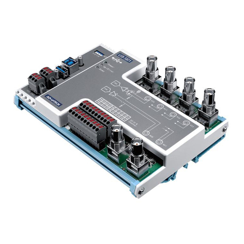
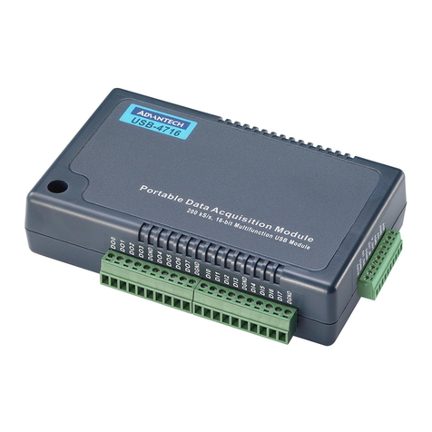
Hardware Installation
After the device driver installation is completed, you can
now go on to install the USB-4716 module in any USB port
that supports the USB 3.0 super speed on your computer.
Please follow the steps below to install the module on your
system:
1. Touch the metal part on the surface of your computer
to neutralize the static electricity that might be in your
body.
2. Plug your USB module into the selected USB port.
Use of excessive force must be avoided; otherwise the
module might get damaged.
Channels 16-ch single-ended/ 8-ch differential
Resolution 16 bits FIFO Size 1024 Samples
Sampling Rate 200 kS/s
Input
Range and
Gain List
Gain 0.5 1 2 4 8
Gain Code 4 0 1 2 3
Bipolar (V) ±10 ±5 ±2.5 ±1.25 ±0.625
Unipolar (V) N/A 0~10 0~5 0~2.5 0~1.25
Drift
Gain 0.5 1 2 4 8
Zero (µV/° C) ±30
Gain (ppm/° C) 30 30 30 30 30
Small Gain 0.5 1 2 4 8
Signal
Bandwidth
for PGA
Bandwidth
(MHz) 1.1 1.1 1.1 1.1 1.1
Input
Protection 30 V max.
Input
Impedance 1GW
Input Comm.
Mode Voltage 11V
Accuracy
DC
INLE 1LSB
DNLE 3LSB
Gain 0.5 1 2 4 8
Gain Error
(% of FSR )
0.015 0.03 0.03 0.05 0.1
AC SINAD 83 dB
THD -88 dB
ENOB 13.5 bit
Channels 2
Resolution 16 bits FIFO Size N/A
Throughput 2 kHz
Operating Mode Single output
Output Range 0~5, 0~10, ±5, ±10 V
Accuracy INLE ±
DNLE ±
Dynamic
Performance
Slew Rate 0.125 V/µs
150 µs (to ±1/2
LSB of FSB)
Driving Capability 5 mA
Output Impedance 0.1W max.
DC
Settling Time
Input Channels 8 Non-Isolation TTL
Input Voltage Low 0.0 Vdc (Min) / 1.0Vdc (Max)
High 2.0 Vdc (Min) / 5.0Vdc (Max)
Output Channels 8 Non-Isolation TTL
Output Voltage Low 0.4 Vdc / -6mA (Sink)
High 2.4 Vdc / 6mA (Source)
Channels 1
Resolution 32-bit base Capability TTL level
Input
Frequency 1 kHz max.
Clock Input Low 0.0 Vdc (Min) / 1.0 Vdc (Max)
High 2.0 Vdc (Min) / 5.0 Vdc (Max)
Gate Input Low 0.0 Vdc (Min) / 1.0 Vdc (Max)
High 2.0 Vdc (Min) / 5.0 Vdc (Max)
I/O Connector Type Removable 10-pin screw terminal x 5
Dimensions 132 X 80 X 32 mm (5.2” X 3.2” X 1.3”)
Power
Consumption 360 mA @ +5.0V Typical
450 mA @ +5.0 V max.
Temperature 0~60° C (32~140° F)
(refer to IEC 68-2-1, 2)
Storage -20~70° C (-4~158° F)
Relative Humidity 5~ 95 % RH non-condensing
(refer to IEC 68-2-1, 2)
Operation
Specifications
Input Channels 8 Non-Isolation TTL
Input Voltage Low 0.0 Vdc (Min) / 1.0Vdc (Max)
High 2.0 Vdc (Min) / 5.0Vdc (Max)
Output Channels 8 Non-Isolation TTL
Output Voltage Low 0.4 Vdc / -6mA (Sink)
High 2.4 Vdc / 6mA (Source)
Channels 1
Resolution 32-bit base Capability TTL level
Input
Frequency 1 kHz max.
Clock Input Low 0.0 Vdc (Min) / 1.0 Vdc (Max)
High 2.0 Vdc (Min) / 5.0 Vdc (Max)
Gate Input Low 0.0 Vdc (Min) / 1.0 Vdc (Max)
High 2.0 Vdc (Min) / 5.0 Vdc (Max)
I/O Connector Type Removable 10-pin screw terminal x 5
Dimensions 132 X 80 X 32 mm (5.2” X 3.2” X 1.3”)
Power
Consumption 360 mA @ +5.0V Typical
450 mA @ +5.0 V max.
Temperature 0~60° C (32~140° F)
(refer to IEC 68-2-1, 2)
Storage -20~70° C (-4~158° F)
Relative Humidity 5~ 95 % RH non-condensing
(refer to IEC 68-2-1, 2)
Operation
Installation
Specications (Cont.) Pin Assignments
