[AKD4688-A]
<KM109900> 2011/12
- 3 -
Operation sequence
1) Set up the power supply lines.
1-1) When AVDD1, AVDD2, DVDD and D3.3V are supplied from the regulator. <Default>
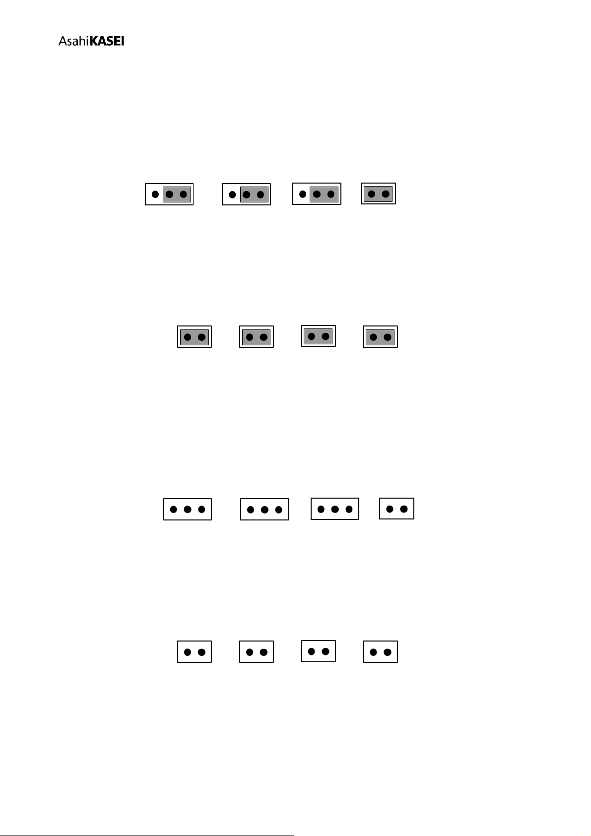
Set up the jumper pins.
JP7
AVDD1_SEL
AVDD1REG
JP8
AVDD2_SEL
AVDD2REG
JP16
D3.3V_SEL
D3.3VREG
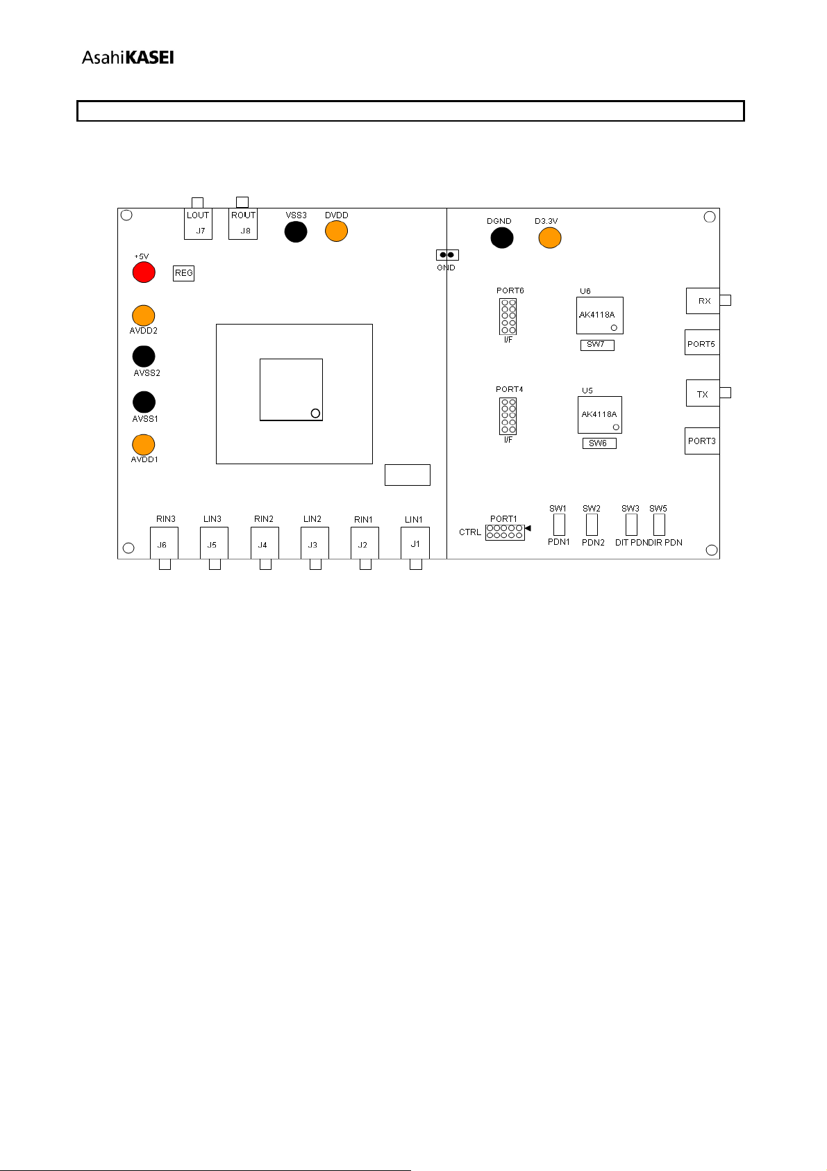
Set up the power supply lines.
Name Color Voltage Comments
+5V Red +5V Power supply for the regulator.
AVDD1 Orange Open Power supply for AVDD1 of AK4688.
AVDD2 Orange Open Power supply for AVDD2 of AK4688.
DVDD Orange Open Power supply for DVDD of AK4688.
D3.3V Orange Open Power supply for logic circuit.
AVSS1 Black 0V Analog ground for ADC of AK4688
AVSS2 Black 0V Analog ground for DAC of AK4688.
VSS3 Black 0V Digital ground of AK4688.
DGND Black 0V Logic circuit ground.
Table 1 Setup of power supply
1-2) When AVDD1, AVDD2, DVDD, and D3.3V are supplied from the power supply connectors.
Set up the jumper pins.
JP7
AVDD1_SEL
AVDD1REG
JP8
AVDD2_SEL
AVDD2REG
JP16
D3.3V_SEL
D3.3VREG
Set up the power supply lines.
Name Color Voltage Comments
+5V Red Open The regulator is not used.
AVDD1 Orange 3.0V~3.6V (typ3.3V) Power supply for AVDD1 of AK4688.
AVDD2 Orange 3.0V~3.6V (typ3.3V) Power supply for AVDD2 of AK4688.
DVDD Orange 3.0V~3.6V (typ3.3V) Power supply for DVDD of AK4688.
D3.3V Orange 3.0V~3.6V (typ3.3V) Power supply for logic circuit.
AVSS1 Black 3.0V~3.6V (typ3.3V) Analog ground for ADC of AK4688
AVSS2 Black 0V Analog ground for DAC of AK4688.
VSS3 Black 0V Digital ground of AK4688.
DGND Black 0V Logic circuit ground.
Table 2 Setup of power supply
* Each supply line should be distributed from the power supply unit.
AVDD1 and AVDD2 should be supplied as the same voltage level.
The difference of voltage level between AVDD1, AVDD2 and DVDD should be under 0.3V.