AKM AKD4589-B User manual

ASAHI KASEI [AKD4589-B]
<KM076201> 2005/07
- 1 -
FEATURE
AKD4589-B is an evaluation board for AK4589, a single chip 24bit CODEC that has two channels of ADC
and eight channels of DAC with internal DIR, DIT. It has interfaces with evaluation boards for A/D
converter and D/A converter of AKM’s and make easy to evaluate AK4589. It also has the digital audio
interface and can achieve the interface with digital audio systems via opt-connector or BNC connector.
Ordering guide
AKD4589-B --- AK4589 Evaluation Board
10 wire flat cable for connection with printer port of PC (IBM-AT compatible
machine),control software for AK4589,driver for control software on Windows
2000/XP are apacked with this.
Control software does not support to I2C control, and does not work on Windows NT
Windows 2000/XP needs an installation of driver.
Windows 95/98/ME does not need an installation of driver.
FUNCTION
On-board clock generator
Compatible with 2 types of interface
- Optical output/input and BNC input
- Direct interface with AC3 decoder by 10pin header
10pin header for serial control interface
Input
Buffer
LIN
RIN
LOUT1
ROUT1
LOUT2
ROUT2
LOUT3
ROUT3
GND
AK4589
10pin Header
10pin Header
Control Data
BNC In
Opt In
Opt Out
AC3
-12V +12V
Output
Buffer
Regulator
BNC Out
Through Out
LOUT4
ROUT4
10pin Header
B, C, U, V
Figure 1. AKD4589-B Block Diagram
* Circuit diagram and PCB layout are attached at the end of this manual.
AK4589 Evaluation Board Rev.2
A
KD4589-B

ASAHI KASEI [AKD4589-B]
<KM076201> 2005/07
- 2 -
EVALUATION BOARD MANUAL
Operation sequence
1) Set up the power supply lines. (See “Other jumpers set-up”.)
Name Color Voltage Used for Comment and attention
+12V Red +12∼+15V Regulator ,I/OBuffer(Op-amp) Power supply for Regulator,I/OBuffer(Op-amp).
It should be always connected.
-12V Blue -12∼-15V I/O Buffer(Op-amp) Power supply for I/OBuffer(Op-amp).
It should be always connected.
AGND Black 0V Analog Ground Analog Ground. It should be always connected.
DGND Black 0V Digital Ground Digital Ground. It should be connected when JP1
is open. This connector can be open when JP1 is
short.
Table 1. Set up of power supply lines
(Note)Each supply line should be distributed from the power supply unit.
2) Set-up of evaluation modes, jumper pins and DIP switches. (See the followings.)
3) Power on
AK4589 should be reset once after power-on of AKD4589-B.
Set SW1 (PDN) “L” once for power down of AK4589 after power-on of AKD4589-B.
And then set SW1 (PDN) “H”.

ASAHI KASEI [AKD4589-B]
<KM076201> 2005/07
- 3 -
Evaluation mode
Applicable evaluation modes
(A) Evaluation of DAC part used internal DIR of AK4589 (See the followings)
(B) Evaluation of ADC part used internal DIT of AK4589 (See the followings)
(A) Evaluation of DAC part used internal DIR of AK4589
1-1. About digital inputs (bi-phase inputs)
1-1-1. Optical connector PORT3 (TORX176,RX0) or BNC connector J12(RX0) are used for digital
inputs(bi-phase inputs) .
1-1-2. Select Optical connector PORT3 (TORX176,RX0) or BNC Connector J12(RX0) for digital inputs
(bi-phase inputs) by JP3 (RX0)
Set JP3(RX0) “OPT” side when Optical connector PORT3(TORX176,RX0) is used for RX0 on
AKD4589-B.
Set JP3(RX0) “BNC” side when BNC connector J12(RX0) is used for RX0 on AKD4589-B.
(See Figure 2)
BNC
JP3
RX0
OPT BNC
JP3
RX0
OPT
or
Using Optical connector
Using BNC
Figure 2. Setting of JP3(RX0) Selection of digital input (bi-phase input)
1-1-3. Write (0,0) into (D5:CM1,D4:CM0) of addr00H:CLK & Power Down Control of control registers of
AK4589 (DIR/DIT) part (CM10=00:Clock Mode=PLL Mode.)
Then clock source is PLL.
(Default setting is PLL. Able to evaluate AK4589 on default setting.)
1-1-4. Set DIP-Switch SW2-2 (MASTER) ON.
Then mode is master mode.
Audio Digital Interface Format is 24bit left justified.
(Please refer to datasheet.).
(Default setting is master mode. Able to evaluate AK4589 on default setting.)
1-2. About analog outputs
1-2-1. BNC connector J2 (LOUT1), J1 (ROUT1), J4 (LOUT2), J3 (ROUT3), J6 (LOUT3), J5 (ROUT3),
J8 (LOUT), J7 (ROUT4) are used for analog outputs.

ASAHI KASEI [AKD4589-B]
<KM076201> 2005/07
- 4 -
(B) ADC Evaluation of using internal DIT of AK4589
2-1. About analog inputs
2-1-1. BNC connectors J10 (LIN),J9 (RIN) are used for analog inputs.
2-2. About digital outputs (bi-phase outputs)
2-2-1. Optical connector PORT2 (TOTX176,TX1) or BNC connector J11 (TX1) are used for digital outputs.
2-2-2. .Select Optical connector PORT2 (TOTX176,TX1) or BNC Connecter J11 (TX1) for digital outputs
(bi-phase outputs) by JP2 (TX1)
Set JP2 (TX1) “OPT” side when Optical connector PORT2(TOTX176,TX1) is used for TX1 on
AKD4589-B.
Set JP2 (TX1) “BNC” side when BNC connector J11(TX1) is used for TX1 on AKD4589-B.
(See Figure3.)
BNC
JP2
TX1
OPT BNC
JP2
TX1
OPT
or
Using Optical connectorUsing BNC
Figure 3. Setting of JP2(TX1) Selection of digital output (bi-phase output)
2-2-3. Write (0,1) into (D5:CM1,D4:CM0) of addr00H:CLK & Power Down Control of control registers of
AK4589 (DIR/DIT) part (CM10=01:Clock Mode=X’tal Mode.)
Then clock source is X’tal (X1).
2-2-4. Set DIP-Switch SW2-2 (MASTER) ON.
Then mode is master mode.
Audio Digital Interface Format is 24bit left justified.
(Please refer to datasheet.).
(Default setting is master mode. Able to evaluate AK4589 on default setting.)

ASAHI KASEI [AKD4589-B]
<KM076201> 2005/07
- 5 -
Setting of DIP-Switch
[SW2]: Setting of AK4589 (SW2:No.2~6 is ON: 1(H), OFF:0(L))
No. Pin OFF ON Default
1 - - - OFF
2 MASTER Slave Mode Master Mode ON(1,H)
3 XTL1 ON(1,H)
4 XTL0 Detection of Sampling frequency (Refer Table 4,5) ON(1,H)
5 CAD1 Setting of Chip Address (ADC/DAC PART) OFF(0,L)
6 CAD0 Setting of Chip Address (ADC/DAC PART) ON(1,H)
Table 2. Setting of SW2
(Note) Chip Address of ADC/DAC is fixed,CAD1,CAD0 is 0(L),1(H). (CAD10=01)
Therefore setting of CAD1,CAD0 is fixed, CAD1,CAD0 is OFF(0,L),ON(1,H).
Sampling frequency as follows
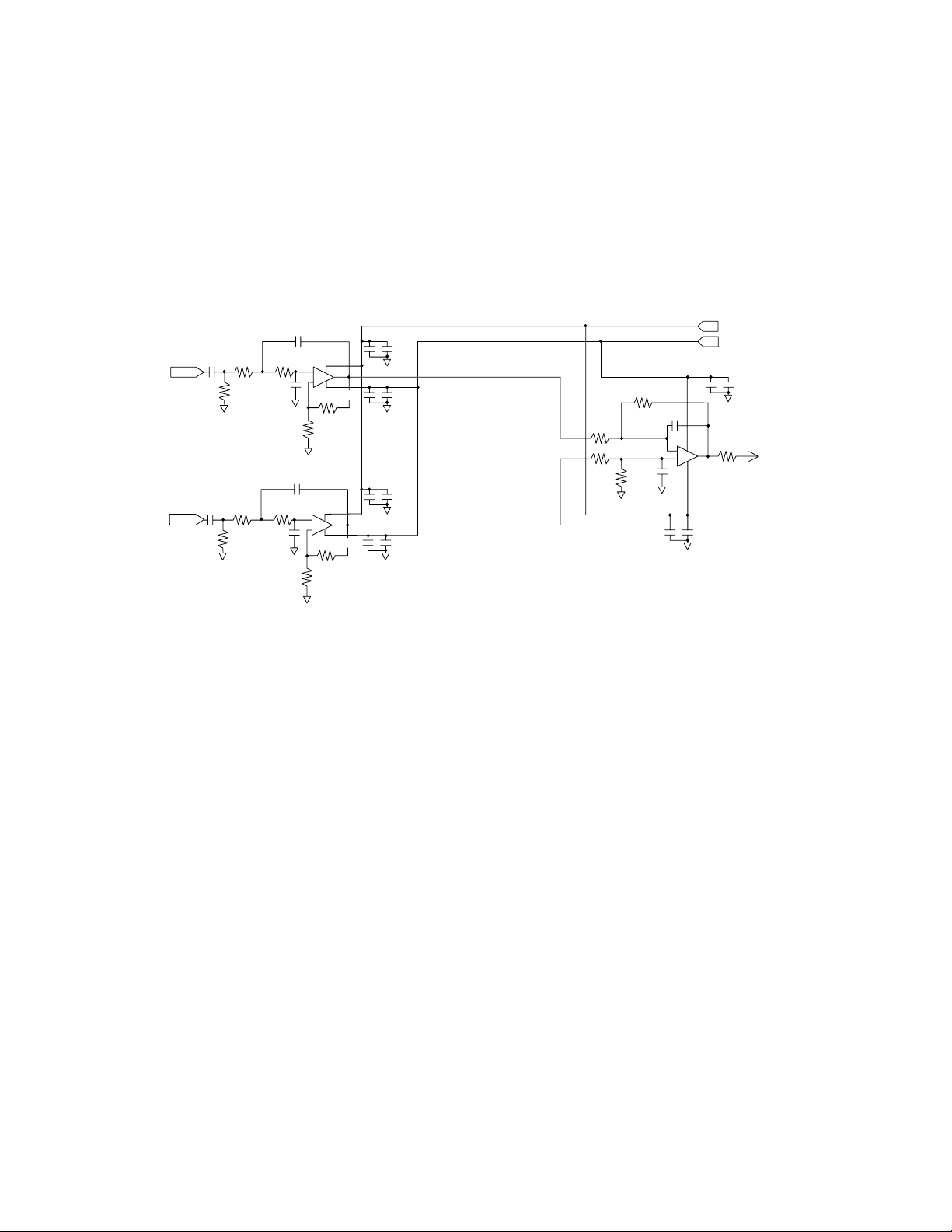
AK4589 has two methods for detecting the sampling frequency. Clock is compared between recovered clock and X’tal
oscillator by XTL1-0. This information outputs FS0, FS1, and FS2, FS3 bit for detecting the sampling frequency.
The compared X’tal frequency is selected by setting of XTL1-0 (Refer Table 4.) When XTL1-0 is ON(1,H),ON(1,H),
X’tal oscillator is stopped and the encored sampling frequency information of channel status output FS0, FS1, FS2, FS3,
PEM bit of resister control.
XTL1 XTL0 X’tal Frequency
OFF(0,L) OFF(0,L) 11.2896MHz
OFF(0,L) ON(1,H) 12.288MHz
ON(1,H) OFF(0,L) 24.576MHz
ON(1,H) ON(1,H) (use channel status)
Default
Table 3. Reference X’tal frequency
Except XTL1,0= “1,1” XTL1, 0= “1,1”
Register output fs Consumer
mode
(Note 2) Professional mode
FS3 FS2 FS1 FS0
Clock comparison
(Note 1) Byte3
Bit3, 2,1,0 Byte0 Bit7,
6 Byte4 Bit6,
5,4,3
0 0 0 0 44.1kHz 44.1kHz 0 0 0 0 0 1 0 0 0 0
0 0 0 1 Reserved Reserved 0 0 0 1 (Others)
0 0 1 0 48kHz 48kHz 0 0 1 0 1 0 0 0 0 0
0 0 1 1 32kHz 32kHz 0 0 1 1 1 1 0 0 0 0
1 0 0 0 88.2kHz 88.2kHz ( 1 0 0 0 ) 0 0 1 0 1 0
1 0 1 0 96kHz 96kHz ( 1 0 1 0 ) 0 0 0 0 1 0
1 1 0 0 176.4kHz 176.4kHz ( 1 1 0 0 ) 0 0 1 0 1 1
1 1 1 0 192kHz 192kHz ( 1 1 1 0 ) 0 0 0 0 1 1
Note1: At least ±3% range is identified as the value in the Table 4. In case of intermediate frequencyof those two, FS3-0
bits indicate nearer value. When the frequency is much bigger than 192kHz or much smaller than 32kHz, FS3-0
bits may indicate “0001”.
Note2: When consumer mode, Byte3 Bit3-0 are copied to FS3-0 bits.
Table 4. Sampling frequency information

ASAHI KASEI [AKD4589-B]
<KM076201> 2005/07
- 6 -
PORT5
ADC/DAC1
2
910
SDTI1
SDTI2
SDTI3
MCKO
BIC
K
LRC
K
SDTO
SDTI4
GND
GND
Jumper setting
[JP1] (GND): Analog grand and digital grand
Open: Analog grand and digital grand are separated.
Short: Analog grand and digital grand are common. “DGND” jack is able to open at this time. < Default>
Operation of toggle switch.
[SW1](PDN): Reset for AK4589.
AK4589 should be reset once after power-on of AKD4589-B.
Set SW1 (PDN) “L” once for power down of AK4589 after power-on of AKD4589-B.
And then set SW1 (PDN) “H”.
Keep “H” during operation of AK4589.
Indication of LED
It turns on each pin when each pin output is “H”.
[LE1] (INT0): Indicate of AK4588’s INT0 pin output.
[LE2] (INT1): Indicate of AK4588’s INT1 pin output.
Serial Control
AK4589 can be controlled via the printer port (parallel port) of IBM-AT compatible PC.
Connect printer port (parallel port) of PC and PORT1(uP-I/F) of AKD4589-B by 10 wire flat cable(packed with
AKD4589-B).
Take care of the direction of 10 pin connector and 10 pin header.
(The red line side of 10 wire flat cable of 10-pin connector should be connected to 5 and 6 pin of 10pin header.)
CSN
SDA / CDTI
SDA(ACK) / CDTO
SCL / CCLK AKD4589-B
10 pin Header
10 pin Connector
10 wire flat cable
Connect
PC
RED
1 10
65 PORT1
uP-I/F
Figure 4. Connection of 10 wire flat cable.
Interface of AC3 decoder
AC3 decoder is able to be interface by using PORT5 (ADC/DAC).
Three serial data is input through PORT5 form AC3 decoder input.
PORT5 pin order is showed Figure 5
Figure 5. PORT5 pin order

ASAHI KASEI [AKD4589-B]
<KM076201> 2005/07
- 7 -
PORT4
BUCV
1
2
910
UOUT
VOUT
VIN
GND
GND
GND
GND
GND
BOUT
COUT
B, U, C, V output and V input
B, U, C, V output and V input is used PORT4 (BUCV).
PORT4 pin order is showed Figure 6.
Figure 6. PORT4 pin order
Analog Inputs
BNC connector J10 (LIN),J9 (RIN) are used for analog inputs on the AKD4589-B. Analog inputs are single-ended
and input ranges of each channels are nominally 6.2Vpp@5V. (Input ranges of each channels of analog inputs of
AK4589 device are nominally 3[email protected],for the resister division,the value which analog input level of
Evaluation Board is devided by two becomes to analog input level of AK4589 device on the AKD4589-B. So, input
ranges of AKD4589-B becomes to 6.2Vpp@5V,twice of the value in the case of AK4589 device. Input range of
AK4589 device is proportional to VREFH (3.1=0.62 x VREFH). VREFH is connected to AVDD on the
AKD4589-B.)
Analog Input Circuit
AK4589
Signal
22u
33RIN
Same circuit
3.1Vpp
NJM4580
-
+
Op-amp circuit
32LIN
6.2Vpp
330
330
Figure 7. Analog Input Circuit
1) Gain
Gain of analog input circuit is
330/(330+330) = -6.02dB.
Therefore input level for this board is
+0.80dBV(=3.1Vpp)+6.02dB
= +6.82dBV = 6.20Vpp = 2.19Vrms.
2) S/N of op-amp circuit (Theory: BW=20k+A)
Non-inverting amp is implemented on board. The output noise level of op-amp circuit is
-126.01dBV = -132.54dB (0dB=+6.53dBV).
S/N of ADC is
101.6dB (measurement).
Therefore total S/N of op-amp circuit and ADC is
101.60dB (measurement: 101.6dB)

ASAHI KASEI [AKD4589-B]
<KM076201> 2005/07
- 8 -
Analog Outputs
BNC connector J2 (LOUT1), J1 (ROUT1), J4 (LOUT2), J3 (ROUT2), J6 (LOUT3), J5 (ROUT3) J8 (LOUT4) ,J7
(ROUT4) are used for analog outputs on the AKD4589-B. Analog outputs are single-ended and output ranges of each
channels are nominally ±3.82Vpp@5V. (Analog outputs of AK4589 device are differencial and output ranges of
each channels are nominally ±2[email protected]ut, input ranges of AKD4589-B becomes to ±3.82Vpp@5V,about
1.41 times of the value in the case of AK4589 device.Output range of AK4589 device is proportional to VREFH
(2.7= 0.54 x VREFH). VREFH is connected to AVDD on the AKD4589-B.)
Analog Output Circuit
330
100u 180
AOUTL-
10k
3.9n
1.2k
680
3.3n
6
4
3
2 7 10u
0.1u
0.1u 10u
10u
NJM4580
330
100u 180
AOUTL+
10k
3.9n
1.2k
680
3.3n
6
4
3
2 7 10u
0.1u
0.1u 10u
NJM4580 0.1u +
NJM4580
0.1u 10u
100
4
3
2
1.0n
620
620
560
7
+
+
++
-
+
-
+
+
+
-
+
+
1.0n
Lch
-15
+15
6
560
Figure 8. Analog Output Circuit
The differential output circuit(2nd order LPF,fc=182KHz,Q=0.637,G=+3.9dB) and LPF(1st order LPF, fc=284KHz,
G=-0.84dB) is implemented on AKD4589-B. The differential outputs of AK4589 is buffered by non-inverted circuit and
output via Cannon connector (differential output). LPF adds differential outputs. NJM4580 is used for op-amp on this
board that has low noise and high voltage torelance characteristics. Analog signal is output via BNC connectors on the
board. The output level is about ±3.82Vpp(typ@VREF=5.0V) by BNC.
* AKM assumes no responsibility for the trouble when using the above circuit examples.

ASAHI KASEI [AKD4589-B]
<KM076201> 2005/07
- 9 -
AKD4589 (DIR/DIT) part Control Program operation manual
Set-up of evaluation board and control software
(Note) Control software does not support to I2C control, and does not work on Windows NT
Windows 2000/XP needs an installation of driver.
Windows 95/98/ME does not need an installation of driver.
Please refer to “Installation Manual of Control Software Driver by AKM device control software”
about the method of installation of driver.
1. Set up the AKD4589-B according to above mentioned setting.
2. Connect printer port(parallel port) of PC and PORT1(up-I/F) of AKD4589-B by 10-wire flat cable packed with
AKD4589. Then take care of the direction of 10pin connector and 10 pin header.
3. Insert the CD-ROM labeled “AK4589-B Control Program ver 2.0” into the CD-ROM drive.
4. Access the CD-ROM drive and double-click the icon of “akd4589-b_dir_dit_2.exe”
and set up the control program.
5. Then evaluate AK4589 (DIR/DIT) part according to the follows.
Operation flow
Keep the following flow.
1. Set up the control program according to explanation above.
2. Click Write default button.
3. Then set up the dialog and input data and evaluate AK4589 (DIR/DIT) part.
Explanation of each buttons
1. [Write default]: Write default data into all registers.
Default data is indicated on the register map of all registers.
Red letter indicates “H” or “1” and blue letter indicates “L” or “0”.
Blank is the part that is not defined in the datasheet.
2. [All Read]: Read data of all registers.
Read data is indicated on the register map of all register.
Red letter indicates “H” or “1” and blue letter indicates “L” or “0”.
Blank is the part that is not defined in the datasheet.
3. [Function1]: Set up dialog to write data by keyboard operation.
4. [Write]: It exists on each register corresponding to all registers.
Set up dialog to write data to each register by mouse operation.
Set ON/OFF by clicking each bits.
Click “OK” button if you write input data to register.
Click “Cancel” button if you don’t write input data to register .
5. [Read]: It exists on each register corresponding to some registers.
Read data from one of each register.
Read data is indicated on the register map of the register.
Red letter indicates “H” or “1” and blue letter indicates “L” or “0”.
Blank is the part that is not defined in the datasheet.

ASAHI KASEI [AKD4589-B]
<KM076201> 2005/07
- 10 -
Explanation of each dialog
1. [Function1 Dialog]:Dialog to write data by keyboard operation
Address Input Box : Input address of register which data should be written into,in 2 figures of hexadecimal.
Data Input Box : Input data which should be written into the register,in 2 figures of hexadecimal.
Click “OK” button,if you write input data into register.
Click “Cancel” button,if you don’t write input data into register.
2. [Write Dialog]: Dialog to write data by mouse operation
There are dialogs corresponding to each register.
Click the “Write” button corresponding to each register to set up the dialog.
If you check the check box, data becomes “H” or “1”. If not, “L” or “0”.
Click “OK” button,if you write input data into register.
Click “Cancel” button,if you don’t write input data into register.
Indication of data
Input data is indicated on the register map.
Red letter indicates “H” or “1” and blue letter indicates “L” or “0”.
Blank is the part that is not defined in the datasheet.
Attention on the operation
Input data to all boxes when you have set up “Function1 dialog”. An “attention dialog” is indicated if you input data or
address that is not specified in the datasheet or you click “OK” button before you input data. In that case set up the dialog
and input data once more again. These operations does not need if you click “Cancel” button or check the check box.

ASAHI KASEI [AKD4589-B]
<KM076201> 2005/07
- 11 -
AK4589 (ADC/DAC) part Control Program Operation Manual
Set-up of evaluation board and control software
(Note) Control software does not support to I2C control, and does not work on Windows NT.
Windows 2000/XP needs an installation of driver.
Windows 95/98/ME does not need an installation of driver.
Please refer to “Installation Manual of Control Software Driver by AKM device control software”
about the method of installation of driver.
1. Set up the AKD4589-B according to above mentioned setting.
2. Connect printer port(parallel port) of PC and PORT1(up-I/F) of AKD4589-B by 10-wire flat cable packed with
AKD4589. Then take care of the direction of 10pin connector and 10 pin header.
3. Insert the CD-ROM-disk labeled “AKD4589 Control Program ver 2.0” into the CD-ROM-disk drive.
4. Access the CD-ROM-disk drive and double-click the icon of “akd4589-b_adc_dac_2.exe” and set up the control
program.
5. Then evaluate AK4589 (ADC/DAC)part according to the followings.
(Note) Chip Address of ADC/DAC is fixed,CAD1,CAD0 is 0(L),1(H). (CAD10=01)
Operation flow
Keep the following flow.
1. Set up the control program according to explanation above
2. Click Write default button.
3. Then set up the dialog and input data and evaluate AK4589 (ADC/DAC) part.
Explanation of each buttons
1. [Write default]: Write default data into all register.
Default data is indicated on the register map of all registers.
Red letter indicates “H” or “1” and blue letter indicates “L” or “0”.
Blank is the part that is not defined in the datasheet.
2. [Function1]: Set up dialog to write data by keyboard operation.
3. [Function2]: Set up dialog to write data by keyboard operation.
4. [Write]: It exists corresponding to each register.
Set up dialog to write data to each register by mouse operation.
Set ON/OFF by clicking each bits.
Click “OK” button if you write input data into register.
Click “Cancel” button if you don’t write input data into register .

ASAHI KASEI [AKD4589-B]
<KM076201> 2005/07
- 12 -
Explanation of each dialog
1. [Function1 Dialog]:Dialog to write data by keyboard operation
Address Input Box : Input address of register which data should be written into,in 2 figures of hexadecimal.
Data Input Box : Input data which should be written into the register,in 2 figures of hexadecimal.
Click “OK” button,if you write input data into register.
Click “Cancel” button,if you don’t write input data into register.
2. [Function2 Dialog]:Dialog to evaluate ATT
This dialog corresponds to addr:02H, 03H,04H, 05H, 06H,07H, 0BH, 0CH.
Address Input Box: Input address of register which data should be written into,in 2 figures of hexadecimal.
Start Data Input Box:Input first data (start data) which should be written into the register,
in 2 figures of hexadecimal.
End Data Input Box: Input last data (end data) which should be written into the register,
in 2 figures of hexadecimal.
Interval Input Box: Input time distance (interval time) between write and write when data is written into the
register,in decimal. Unit of time is ms.
Step Input Box: Input value distance (step of data) between data and data when data is written into the register,
in decimal.
Mode Select Check Box:Select mode of data flow, “Data returns to start data after data reached end data.”
Or “Data flow is end when data reached end data.”
Set mode of data flow by checked or no into this check box.
When you checked into this: Data returns to start data after data reached end data.
When you did not check into this: Data flow is end when data reached end data.
[Example When you checked into this] Start Data = 00, End Data = 09
Data flow: 00 01 02 03 04 05 06 07 08 09 09 08 07 06 05 04 03 02 01 00
[Example When you did not check into this] Start Data = 00, End Data = 09
Data flow: 00 01 02 03 04 05 06 07 08 09
Click “OK” button,if you write input data into register.
Click “Cancel” button,if you don’t write input data into register.
3. [Write Dialog]: Dialog to write data by mouse operation
There are dialogs corresponding to each register.
Click the “Write” button corresponding to each register to set up the dialog.
If you check the check box, data becomes “H” or “1”. If not, “L” or “0”.
Click “OK” button,if you write input data into register.
Click “Cancel” button,if you don’t write input data into register.
Indication of data
Input data is indicated on the register map.
Red letter indicates “H” or “1” and blue letter indicates “L” or “0”.
Blank is the part that is not defined in the datasheet.
Attention on the operation
Input data to all boxes when you have set up “Function1 dialog” or “Function2 dialog”. An “attention dialog” is indicated
if you input data or address that is not specified in the datasheet or you click “OK” button before you input data. In that case
set up the dialog and input data once more again.These operations does not need if you click “Cancel” button or check the
check box.

ASAHI KASEI [AKD4589-B]
<KM076201> 2005/07
- 13 -
Measure Result
1) ADC part
[Measurement condition]
•Measurement unit: Audio Precision System two Cascade (AP2)
•MCLK : 256fs (fs=48kHz), 256fs (fs=96kHz)
•BICK :64fs
•fs :48kHz,96kHz
•BW :20Hz∼20kHz (fs=48kHz), 20Hz∼40kHz (fs=96kHz)
•Bit : 24bit
•Power Supply : AVDD=PVDD=DVDD=5V, TVDD=3.3V
•Interface : Internal DIT (fs=48kHz, 96kHz)
•Temperature : Room Temp
fs=48kHz
Parameter Input signal Measurement filter Results
S/(N+D) 1kHz, -0.5dB 20kLPF 94.4 dB
DR 1kHz, -60dB 20kLPF 98.5 dB
DR 1kHz, -60dB 20kLPF, A-weighted 101.2 dB
S/N No signal 20kLPF 98.8 dB
S/N No signal 20kLPF, A-weighted 101.6 dB
fs=96kHz
Parameter Input signal Measurement filter Results
S/(N+D) 1kHz, -0.5dB fs/2 92.1 dB
DR 1kHz, -60dB fs/2 97.6 dB
DR 1kHz, -60dB 20kLPF, A-weighted 104.4 dB
S/N No signal fs/2 97.6 dB
S/N No signal 20kLPF, A-weighted 104.8 dB

ASAHI KASEI [AKD4589-B]
<KM076201> 2005/07
- 14 -
2) DAC part
[Measurement condition]
•Measurement unit: Audio Precision System two Cascade (AP2)
•MCLK : 256fs (fs=48kHz, 96kHz), 128fs (fs=192kHz)
•BICK :64fs
•fs : 48kHz, 96kHz, 192kHz
•BW :20Hz
∼20kHz (fs=48kHz), 20Hz∼40kHz (fs=96kHz), 20Hz∼40kHz (fs=192kHz)
•Resolution : 24bit
•Power Supply : AVDD=PVDD=DVDD=5V, TVDD=3.3V
•Interface : Internal DIR (48kHz, 96kHz, 192kHz)
•Temperature : Room Temp
fs=48kHz
Parameter Input signal Measurement filter Results
S/(N+D) 1kHz, 0dB 20kLPF 98.7 dB
DR 1kHz, -60dB 20kLPF 110.0 dB
DR 1kHz, -60dB 22kLPF, A-weighted 112.5 dB
S/N “0” data 20kLPF 110.0 dB
S/N “0” data 22kLPF, A-weighted 112.8 dB
fs=96kHz
Parameter Input signal Measurement filter Results
S/(N+D) 1kHz, 0dB 40kLPF 97.8 dB
DR 1kHz, -60dB 40kLPF 106.8 dB
DR 1kHz, -60dB 22kLPF, A-weighted 112.2 dB
S/N “0” data 40kLPF 106.8 dB
S/N “0” data 22kLPF, A-weighted 112.5 dB
fs=192kHz
Parameter Input signal Measurement filter Results
S/(N+D) 1kHz, 0dB 40kLPF 96.4 dB
DR 1kHz, -60dB 40kLPF 106.8 dB
DR 1kHz, -60dB 22kLPF, A-weighted 112.2 dB
S/N “0” data 40kLPF 107.0 dB
S/N “0” data 22kLPF, A-weighted 112.5 dB

ASAHI KASEI [AKD4589-B]
<KM076201> 2005/07
- 15 -
Plots
1) ADC
[Measurement condition]
•Measurement Unit : Audio Precision System two Cascade
•MCLK : 256fs(fs=48kHz), 256fs(fs=96kHz)
•BICK :64fs
•fs :48kHz,96kHz
•BW :20Hz∼20kHz (fs=48kHz), 40Hz∼40kHz (fs=96kHz)
•Resolution :24bit
•Power Supply : AVDD=PVDD=DVDD=5V, TVDD=3.3V
•Interface : Internal DIT (fs=48kHz, 96kHz)
•Temperatur : Room Temp
fs=48kHz
Figure 7. FFT (Input Frequency =1kHz, Input Level =0dBFS)
Figure 8. FFT (Input Frequency =1kHz, Input Level =-60dBFS)
Figure 9. FFT (noise floor)
Figure 10. THD+N vs Input Level (Input Frequency =1kHz)
Figure 11. THD+N vs Input Frequency (Input Level=0dBFS)
Figure 12. Linearity (Input Frequency =1kHz)
Figure 13. Frequency Response (Input Level=0dBFS)
Figure 14. Cross-talk (Input Level=0dBFS)
fs=96kHz
Figure 15. FFT (Input Frequency =1kHz, Input Level =0dBFS)
Figure 16. FFT (Input Frequency =1kHz, Input Level =-60dBFS)
Figure 17. FFT (noise floor)
Figure 18. THD+N vs Input Level (Input Frequency =1kHz)
Figure 19. THD+N vs fin (Input Level=0dBFS)
Figure 20. Linearity (Input Frequency =1kHz)
Figure 21. Frequency Response (Input Level=0dBFS)
Figure 22. Cross-talk (Input Level=0dBFS)
FFT point=16384, Avg=8, Window=Equirriple

ASAHI KASEI [AKD4589-B]
<KM076201> 2005/07
- 16 -
2) DAC
[Measurement Condition]
•Measurement Unit : Audio Precision System two Cascade
•MCLK : 256fs(fs=48kHz), 256fs(fs=96kHz), 128fs(fs=192kHz)
•BICK :64fs
•fs : 48kHz, 96kHz, 192kHz
•BW :20Hz
∼20kHz (fs=48kHz), 40Hz∼40kHz (fs=96kHz), 40Hz∼80kHz (fs=192kHz)
•Resolution :24bit
•Power Supply : AVDD=PVDD=DVDD=5V, TVDD=3.3V
•Interface : Internal DIR (48kHz, 96kHz, 192kHz)
•Temperature : Room Temp
fs=48kHz
Figure 23. FFT (Input Frequency =1kHz, Input Level =0dBFS)
Figure 24. FFT (Input Frequency =1kHz, Input Level =-60dBFS)
Figure 25. FFT (noise floor)
Figure 26. FFT (out-of-band noise)
Figure 27. THD+N vs Input Level (Input Frequency =1kHz)
Figure 28. THD+N vs Input Frequency (Input Level=0dBFS)
Figure 29. Linearity (Input Frequency =1kHz)
Figure 30. Frequency Response (Input Level=0dBFS)
Figure 31. Cross-talk (Input Level=0dBFS)
fs=96kHz
Figure 32. FFT (Input Frequency =1kHz, Input Level =0dBFS)
Figure 33. FFT (Input Frequency =1kHz, Input Level =-60dBFS)
Figure 34. FFT (noise floor)
Figure 35. FFT (out-of-band noise)
Figure 36. THD+N vs Input Level (Input Frequency =1kHz)
Figure 37. THD+N vs fin (Input Level=0dBFS)
Figure 38. Linearity (Input Frequency =1kHz)
Figure 39. Frequency Response (Input Level=0dBFS)
Figure 40. Cross-talk (Input Level=0dBFS)
fs=192kHz
Figure 41. FFT (Input Frequency =1kHz, Input Level =0dBFS)
Figure 42. FFT (Input Frequency =1kHz, Input Level =-60dBFS)
Figure 43. FFT (noise floor)
Figure 44. FFT (out-of-band noise)
Figure 45. THD+N vs Input Level (Input Frequency =1kHz)
Figure 46. THD+N vs fin (Input Level=0dBFS)
Figure 47. Linearity (Input Frequency =1kHz)
Figure 48. Frequency Response (Input Level=0dBFS)
Figure 49. Cross-talk (Input Level=0dBFS)
FFT point=16384, Avg=8, Window=Equirriple

ASAHI KASEI [AKD4589-B]
<KM076201> 2005/07
- 17 -
1.ADC (ADC fs=48kHz)
AKM Red=Lch,Blue=Rch
-160
+0
-150
-140
-130
-120
-110
-100
-90
-80
-70
-60
-50
-40
-30
-20
-10
d
B
F
S
20 20k50 100 200 500 1k 2k 5k 10k
Hz
Figure 8. FFT(Input Frequency=1kHz,Input Level=-0.5dBFS)
AKM Red=Lch,Blue=Rch
-160
+0
-150
-140
-130
-120
-110
-100
-90
-80
-70
-60
-50
-40
-30
-20
-10
d
B
F
S
20 20k50 100 200 500 1k 2k 5k 10k
Hz
Figure 9. FFT(Input Frequency=1kHz,Input Level=-60dBFS)

ASAHI KASEI [AKD4589-B]
<KM076201> 2005/07
- 18 -
(ADC fs=48kHz)
AKM Red=Lch,Blue=Rch
-160
+0
-150
-140
-130
-120
-110
-100
-90
-80
-70
-60
-50
-40
-30
-20
-10
d
B
F
S
20 20k50 100 200 500 1k 2k 5k 10k
Hz
Figure 10. FFT(noise floor)
AKM Red=Lch,Blue=Rch
-140 +0-130 -120 -110 -100 -90 -80 -70 -60 -50 -40 -30 -20 -10
dBr
-120
-80
-118
-116
-114
-112
-110
-108
-106
-104
-102
-100
-98
-96
-94
-92
-90
-88
-86
-84
-82
d
B
F
S
Figure 11. THD + N vs Input Level(Input Frequency=1kHz)

ASAHI KASEI [AKD4589-B]
<KM076201> 2005/07
- 19 -
(ADC fs=48kHz)
AKM Red=Lch,Blue=Rch
20 20k50 100 200 500 1k 2k 5k 10k
Hz
-120
-80
-118
-116
-114
-112
-110
-108
-106
-104
-102
-100
-98
-96
-94
-92
-90
-88
-86
-84
-82
d
B
F
S
Figure 12. THD + N vs Input Frequency (Input Level=-0.5dBFS)
AKM Red=Lch,Blue=Rch
-140 +0-130 -120 -110 -100 -90 -80 -70 -60 -50 -40 -30 -20 -10
dBr
-140
+0
-130
-120
-110
-100
-90
-80
-70
-60
-50
-40
-30
-20
-10
d
B
F
S
TT
Figure 13. Linearity (Input Frequency=1kHz)

ASAHI KASEI [AKD4589-B]
<KM076201> 2005/07
- 20 -
(ADC fs=48kHz)
AKM Red=Lch,Blue=Rch
20 20k50 100 200 500 1k 2k 5k 10k
Hz
-1
+0
-0.95
-0.9
-0.85
-0.8
-0.75
-0.7
-0.65
-0.6
-0.55
-0.5
-0.45
-0.4
-0.35
-0.3
-0.25
-0.2
-0.15
-0.1
-0.05
d
B
F
S
Figure 14. Frequency Response(including input RC filter) (Input Level=-0.5dBFS)
AKM Red=Rch->Lch,Blue=Lch->Rch
20 20k50 100 200 500 1k 2k 5k 10k
Hz
-150
-80
-145
-140
-135
-130
-125
-120
-115
-110
-105
-100
-95
-90
-85
d
B
T
Figure 15. Crosstalk (Upper@1k = Rch, Lower@1k = Lch)
Table of contents
Other AKM Motherboard manuals