PT-5IV SYSTEM BOARD HARDWARE SETUP
4. HARDWARE SETUP
4.1 UNPACKING
The system board package should contain the following parts :
The PT-5IV system board.
OPERATION MANUAL.
Cable set for IDE and I/O device.
4.2 HARDWARE CONFIGURATION
Before the system board is ready to operate, the hardware must be configured to allow for various functions
within the system. To configure the PT-5IV system board is a simple task, only a few jumpers, connectors,
cables and sockets needs to be selected and installed. (For the detailed locations of each component please refer
to the "system board layout figure" which appears in page 3-1.)
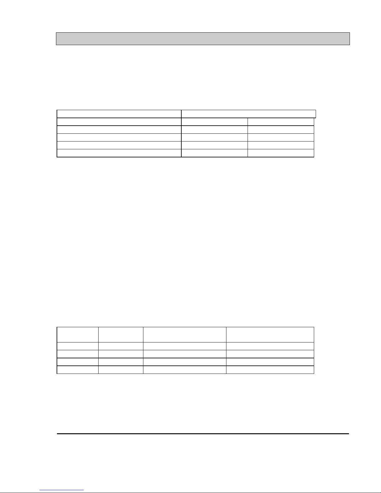
4.2.1 DRAM INSTALLATION
The PT-5IV system board will support two banks main memory (bank0 and bank 1) on board, (using four 72-
Pin SIMM socket, SIMM 1 - 4 and one 168-pin DIMM socket, DIMM 1) each bank could be single-sided or
double-sided, 8MB up to 128 MB of local memory can be attained. Supports standard fast page mode (FPM),
Extended Data Out (EDO) and synchronous (SDRAM) memory.
The usable DRAM modules are : (Note : S = Single-sided , D = Double-sided)
(1)FPM and EDO memory : 1MBx32(36)-S ( 4MB) ,1MBx32(36)-D ( 8MB),
2MBx32(36)-S ( 8MB) , 2MBx32(36)-D (16MB),
4MBx32(36)-S (16MB) , 4MBx32(36)-D (32MB).
(2) SDRAM memory : 1MBx64-S (8MB) , 2MBx64-D (16MB) , 4MBx64-S (32MB).
The speed of FPM DRAMs must be used 70ns or faster than 70ns, the speed of EDO DRAMs and SDRAMs
must be used 60ns or faster than 60ns.
SIMMs' and DIMM's operating voltage :
(1)SIMM1 - SIMM4 : + 5V DC
(2)DIMM1 : +3.3V / +3.4V / +3.5V DC (depends on CPU I/O voltage, refer to page 4-8 )
Bank can be populated in any order (bank 0 does not have to be populated before bank 1). Within any given
bank, the SIMMs (DIMM) must be the same size. Among the two banks, SIMM (DIMM) densities can be
mixed in any order. EDO, FPM and SDRAMs can be mixed between SIMMs (DIMM), a given SIMM (DIMM)
must contain only one type of DRAM. When DRAM types are mixed each SIMM (DIMM) runs optimized for
that particular type of DRAM.
4-1