ECS P4VXAD+ User manual

Preface
Copyright
This publication, including all photographs, illustrations and software, is protected un-
der international copyright laws, with all rights reserved. Neither this manual, nor any
of the material contained herein, may be reproduced without written consent of the au-
thor.
Version 1.0a
Disclaimer
The information in this document is subject to change without notice. The manufac-
turer makes no representations or warranties with respect to the contents hereof and
specifically disclaim any implied warranties of merchantability or fitness for any
particular purpose. The manufacturer reserves the right to revise this publication and
to make changes from time to time in the content hereof without obligation of the
manufacturer to notify any person of such revision or changes.
Trademark Recognition
Microsoft, MS-DOS and Windows are registered trademarks of Microsoft Corp.
MMX, Pentium, Pentium-II, Pentium-III, Celeron are registered trademarks of Intel
Corporation.
Other product names used in this manual are the properties of their respective owners
and are acknowledged.
Federal Communications Commission (FCC)
This equipment has been tested and found to comply with the limits for a Class B digi-
tal device, pursuant to Part 15 of the FCC Rules. These limits are designed to provide
reasonable protection against harmful interference in a residential installation. This
equipment generates, uses, and can radiate radio frequency energy and, if not in-
stalled and used in accordance with the instructions, may cause harmful interference
to radio communications. However, there is no guarantee that interference will not oc-
cur in a particular installation. If this equipment does cause harmful interference to
radio or television reception, which can be determined by turning the equipment off
and on, the user is encouraged to try to correct the interference by one or more of the
following measures:
− Reorient or relocate the receiving antenna.
− Increase the separation between the equipment and the receiver.
− Connect the equipment onto an outlet on a circuit different from that to which
the receiver is connected.
− Consult the dealer or an experienced radio/TV technician for help.
Shielded interconnect cables and a shielded AC power cable must be employed with
this equipment to ensure compliance with the pertinent RF emission limits governing
this device. Changes or modifications not expressly approved by the system's manu-
facturer could void the user's authority to operate the equipment.
i

Declaration of Conformity
This device complies with part 15 of the FCC rules. Operation is subject to the follow-
ing conditions:
− This device may not cause harmful interference, and
− This device must accept any interference received, including interference
that may cause undesired operation.
Canadian Department of Communications
This class B digital apparatus meets all requirements of the Canadian Interference-
causing Equipment Regulations.
Cet appareil numérique de la classe B respecte toutes les exigences du Réglement
sur le matériel brouilieur du Canada.
About the Manual
The manual consists of the following:
Chapter 1
Introducing the Mainboard Describes features of the mainboard,
and provides a shipping checklist.
Go to ⇒page 1
Chapter 2
Installing the Mainboard Describes installation of mainboard
components.
Go to ⇒page 7
Chapter 3
Using BIOS Provides information on using the BIOS
Setup Utility.
Go to ⇒page 28
Chapter 4
Using the Mainboard Software Describes the mainboard software.
Go to ⇒page 53
ii

T
TA
AB
BL
LE
E
O
OF
F
C
CO
ON
NT
TE
EN
NT
TS
S
Preface i
Features and Packing List Translations 錯誤! 尚未定義書籤。
CHAPTER 1 1
Introducing the Mainboard 1
Introduction................................................................................................ 1
Checklist.................................................................................................... 1
Standard Items................................................................................................. 1
Features .................................................................................................... 2
Choosing a Computer Case....................................................................... 4
Mainboard Components ............................................................................ 5
CHAPTER 2 7
Installing the Mainboard 7
Safety Precautions..................................................................................... 7
Quick Guide............................................................................................... 7
Installing the Mainboard in a Case............................................................. 8
Checking Jumper Settings......................................................................... 8
Setting Jumpers ............................................................................................... 8
Checking Jumper Settings ............................................................................... 9
Jumper Settings ............................................................................................... 9
Connecting Case Components................................................................ 11
Front Panel Connector................................................................................... 13
Installing Hardware.................................................................................. 14
Installing the Processor.................................................................................. 14
Installing Memory Modules .......................................................................... 17
Installing a Hard Disk Drive/CD-ROM......................................................... 18
Installing a Floppy Diskette Drive................................................................. 20
Installing Add-on Cards................................................................................. 20
Connecting Optional Devices........................................................................ 22
Connecting I/O Devices........................................................................... 26
External Connector Color Coding................................................................. 27
CHAPTER 3 28
Using BIOS 28
About the Setup Utility............................................................................. 28
The Standard Configuration........................................................................... 28
Entering the Setup Utility.............................................................................. 29
Updating the BIOS........................................................................................ 29
Using BIOS.............................................................................................. 30
Standard CMOS Features.............................................................................. 31
Advanced BIOS Setup Option....................................................................... 33
iii

Advanced Chipset Features Option ............................................................... 35
Integrated Peripherals Option........................................................................ 40
Power Management Setup Option................................................................. 44
PNP/PCI Configurations................................................................................ 48
PC Health Status Option................................................................................ 50
Frequency/Voltage Control............................................................................ 50
Load Fail-Safe Defaults Option..................................................................... 51
Load Optimized Defaults Option................................................................... 51
Set Password Option...................................................................................... 52
Save & Exit Setup Option.............................................................................. 52
Exit Without Saving....................................................................................... 52
CHAPTER 4 53
Using the Mainboard Software 53
About the Software CD-ROM................................................................... 53
Auto-installing under Windows 98/ME/2000/XP....................................... 53
Running Setup............................................................................................... 54
Manual Installation................................................................................... 56
Utility Software Reference....................................................................... 56
iv

C
Ch
ha
ap
pt
te
er
r
1
1
Introducing the Mainboard
I
In
nt
tr
ro
od
du
uc
ct
ti
io
on
n
Thank you for choosing the P4VXAD+ mainboard. The P4VXAD+ mainboard
is an ATX mainboard that uses a 4-layer printed circuit board and measures
305 mm x 244 mm. The mainboard features a Socket 478 that accommodates
Intel Pentium 4 processors supporting front side bus (FSB) speeds of 400/533
MHz (133 MHz QDR).
This mainboard incorporates the VIA P4X333 Northbridge and VT8235
Southbridge chipsets which supports the AC 97 audio codec, which combines
support for DDR (Double Data Rate) SDRAM up to 3 GB (registered)/1.5 GB
(unbuffered).
The P4VXAD+ is designed to give customers an advanced, multimedia solu-
tion at a very low cost. It is equipped with advanced full set of I/O ports, such
as dual channel IDE interfaces, a floppy controller, two high-speed serial port,
an EPP/ECP capable bi-directional parallel port connector, four USB (Univer-
sal Serial Bus) connector, a PS/2 keyboard, and mouse connectors. One AGP
slot, five PCI local bus slots and one communication and networking riser
(CNR) slot provide expandability for add-on peripheral cards.
C
Ch
he
ec
ck
kl
li
is
st
t
Compare the mainboard’s package contents with the following checklist:
Standard Items
• One mainboard
• One diskette drive ribbon cable
• One IDE drive ribbon cable
• One retention module
• Software support CD
• This user’s manual
1
F
Fe
ea
at
tu
ur
re
es
s
Processor The P4VXAD+ mainboard includes a mPGA Socket 478 that
has the following features:
• Supports up to a 400/533 MHz (133 MHz QDR) front side
bus (FSB)
• Accommodates Intel Pentium 4 processors
Chipset The chipset on P4VXAD+ includes the P4X333 Northbridge and
VT8235 Southbridge which are based on an innovative and scal-
able architecture with proven reliability and performance. A few of
the chipset’s advanced features are:
• High performance Northbridge with 533 MHz Front Side
Bus for Pentium 4
• 64-bit Advanced ECC Memory controller supporting
PC2700/PC2100/PC1600 DDR SDRAM
• Combines with VIA VT8235 V-Link Southbridge for inte-
grated LAN, Audio and ATA133 IDE
• Supports 266 MHz 4x and 133 MHz 2x transfer modes for
AD and SBA signaling
• AGP v2.0 compliant with 4x transfer mode compliant
• DRAM interface pseudo-synchronous with host CPU
(100/133 MHz) for most flexible configuration
• Supports 66 MHz V-Link Client interface with peak band-
width of 266 MB/sec
• Integrated Fast Ethernet Controller with 1 / 10 / 100 Mbit
capability
• PCI to system memory data streaming up to 132 Mbyte/s
(data sent to north bridge via high speed V-Link Interface)
• USB v2.0 and Universal Host Controller Interface (UHCI)
v2.0 compatible
Additional features include support for six USB ports, an AC 97
link for audio and modem, hardware monitoring, and
ACPI/OnNow power management.
Memory The mainboard accommodates three 184 pin, 2.5V DDR DIMM
sockets with a total capacity of 3 GB (registered)/1.5 GB (un-
buffered).
AGP The P4VXAD+ includes a 4xAGP slot that provides four times
the bandwidth of the original AGP specification. AGP technol-
ogy provides a direct connection between the graphics sub-
system and memory so that the graphics do not have to com-
pete for processor time with other devices on the PCI bus.
AC’ 97 Audio
Codec
• Compliant with AC’97 (Rev 2.2) CODEC, meet PC2001
requirements
• Analog switch for Rear-out share the Line-in jack and
Center/Bass share the MIC jack to output 6 channels
audio
• Built-in earphone buffer and internal PLL
• Digital S/PDIF IN/OUT support
2

Expansion
Options The mainboard comes with the following expansion options:
• Five 32-bit PCI slots
• One 4xAGP slot
• A Communications Network Riser (CNR) slot (AC97 inter-
face only)
• Two IDE connectors which support four IDE channels and
a floppy disk drive interface
• IDE RAID 1, 0 supported by Promise PDC20265R con-
troller (optional)
The P4VXAD+ are capable of Ultra DMA bus mastering with
transfer rates of 33/66/100/133 MB/sec.
Onboard LAN
(optional)
The VT6103 is a Physical Layer device for Ethernet 10BASE-T
and 100BASE-TX using category 5 Unshielded, Type 1
Shielded, and Fiber Optic cables.
• Dual Speed – 100/10 Mbps
• Half And Full Duplex
• Meet All Applicable IEEE 802.3, 10Base-T and 100Base-
Tx Standards
• Adaptive Equalizer
Promise 20265
(optional)
• Supports Ultra ATA100 drives and backward compatible
with Ultra ATA66/33 & EIDE drives (identical drives rec-
ommended)
• Supports IDE RAID 1(mirroring) or 0 (striping)
• Supports UDMA 5/4/3/2/1/0, DMA 2/1/0, PIO 4/3/2/1/0
modes
• Two independent IDE channels support up to four
UDMA/100/66/33 or EIDE drives
Integrated I/O The mainboard has a full set of I/O ports and connectors:
• Two PS/2 ports for mouse and keyboard
• Two serial port
• One parallel port
• One MIDI/game port
• Six USB ports (two backpanel ports, onboard USB head-
ers providing four extra ports)
• Audio jacks for microphone, line-in and line-out
BIOS
Firmware This mainboard uses Award BIOS that enables users to con-
figure many system features including the following:
• Power management
• CPU and memory timing
• Modem wake up alarms
The firmware can also be used to set parameters for different
processor clock speeds.
3

C
Ch
ho
oo
os
si
in
ng
g
a
a
C
Co
om
mp
pu
ut
te
er
r
C
Ca
as
se
e
There are many types of computer cases on the market. The mainboard com-
plies with the specifications for the ATX system case. Some features on the
mainboard are implemented by cabling connectors on the mainboard to indi-
cators and switches on the system case. Ensure that your case supports all
the features required. The mainboard can support one floppy diskette drive
and four enhanced IDE drives. Ensure that your case has sufficient power and
space for all the drives that you intend to install.
Most cases have a choice of I/O templates in the rear panel. Make sure that
the I/O template in the case matches the I/O ports installed on the rear edge
of the mainboard.
This mainboard has an ATX form factor of 305 x 244 mm. Choose a case that
accommodates this form factor.
4

M
Ma
ai
in
nb
bo
oa
ar
rd
d
C
Co
om
mp
po
on
ne
en
nt
ts
s
5

Table of Mainboard Components
Label Component
AGP1 Accelerated Graphics Port
ATX1 Power connector
AUDIO Mic/speaker-out connector
BT1 Three volt realtime clock battery
CASFAN Auxiliary case cooling fan
CD1 Primary CD-in connector (Sony)
CD2 Secondary CD-in connector (Panasonic)
CNR1 Communications Networking Riser slot
CPU SOCKET CPU Socket (mPGA478)
CPUFAN Cooling fan for CPU
DDRDIMM1 ~ DDRDIMM3 Three 184-pin DDR DIMM sockets
FDD1 Floppy disk drive connector
IDE 1 Primary IDE channel
IDE 2 Secondary IDE channel
IDE 3 Third IDE channel for ATA 66/100
IDE 4 Fourth IDE channel for ATA 66/100
J3 Single-color LED header
JP1 Clear CMOS jumper
JP2 BIOS protect jumper
JP3 CPU frequency select jumper
JP4 CPU voltage adjustment jumper
LED1 LED 2.5 VSB for DDR SDRAM (red)
PANEL Panel connector for case switches and LEDs
PCI1 ~ PCI5 Five 32-bit add-on card slots
RAIDLED IDE3/IDE4 array controller active LED
SIR Serial infrared cable header
SJ1 Single-color LED header
SMI External System Management Interrupt header
USB2 ~ USB3 Connector for front panel USB ports
Note: LED1 is usually connected to a light that indicates that the computer is
powered on. Do not install hardware or disconnect power cables while the
LED is on.
This concludes Chapter 1. The next chapter explains how to install the main-
board.
6

C
Ch
ha
ap
pt
te
er
r
2
2
Installing the Mainboard
S
Sa
af
fe
et
ty
y
P
Pr
re
ec
ca
au
ut
ti
io
on
ns
s
Follow these safety precautions when installing the mainboard:
• Wear a grounding strap attached to a grounded device to avoid
damage from static electricity.
• Discharge static electricity by touching the metal case of a safely
grounded object before working on the mainboard.
• Leave components in the static-proof bags they came in.
• Hold all circuit boards by the edges. Do not bend circuit boards.
Q
Qu
ui
ic
ck
k
G
Gu
ui
id
de
e
This Quick Guide suggests the steps you can take to assemble your system
with the mainboards.
The following table provides a reference for installing specific components:
Locating Mainboard Components Go to page 5
Installing the Mainboard in a Case Go to page 8
Setting Jumpers Go to page 8
Installing Case Components Go to page 11
Installing the CPU Go to page 14
Installing Memory Go to page 17
Installing a HDD and CD-ROM Drive Go to page 18
Installing a FDD Go to page 20
Installing Add-on Cards Go to page 20
Connecting Options Go to page 22
Connecting Peripheral (I/O) Devices Go to page 26
7

I
In
ns
st
ta
al
ll
li
in
ng
g
t
th
he
e
M
Ma
ai
in
nb
bo
oa
ar
rd
d
i
in
n
a
a
C
Ca
as
se
e
Refer to the following illustration and instructions for installing the mainboard
in a case:
This illustration shows an ex-
ample of a mainboard being
installed in a tower-type case:
Note: Do not overtighten
the screws as this
can stress the main-
board.
Most system cases have
mounting brackets installed in
the case, which correspond to
the holes in the mainboard.
Place the mainboard over the
mounting brackets and secure
the mainboard onto the mount-
ing brackets with screws.
2. Secure the mainboard with
screws where appropriate.
1. Place the mainboard
over the mounting brackets.
Ensure that your case has an I/O template that supports the I/O ports and
expansion slots on your mainboard.
C
Ch
he
ec
ck
ki
in
ng
g
J
Ju
um
mp
pe
er
r
S
Se
et
tt
ti
in
ng
gs
s
This section explains how to set jumpers for correct configuration of the main-
board.
Setting Jumpers
Use the mainboard jumpers to set system configuration options. Jumpers with
more than one pin are numbered. When setting the jumpers, ensure that the
jumper caps are placed on the correct pins.
The illustrations below show a 2-pin jumper.
When the jumper cap is placed on both pins,
the jumper is SHORT. If you remove the
jumper cap, or place the jumper cap on just
one pin, the jumper is OPEN.
This illustration shows a 3-pin
jumper. Pins 1 and 2 are SHORT.
Short Open
123
8
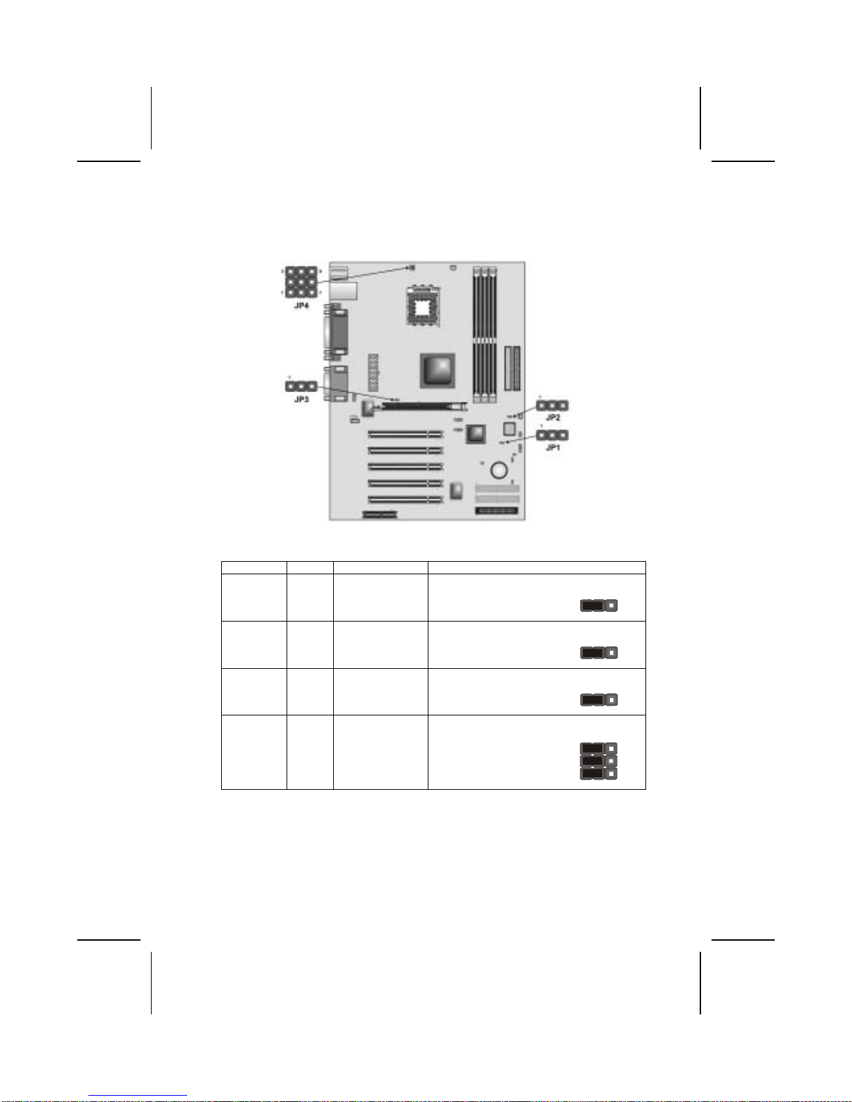
Checking Jumper Settings
The following illustration shows the location of the mainboard jumpers. Pin 1 is
labeled.
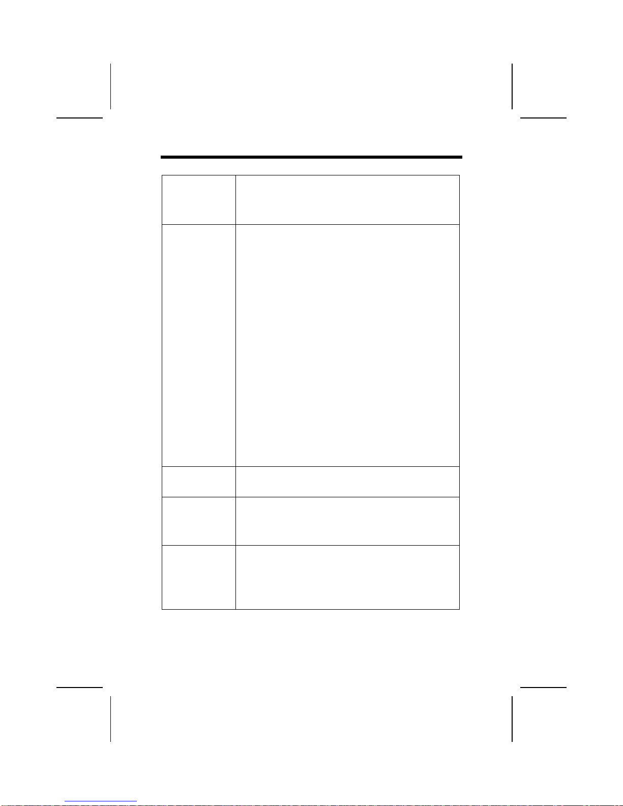
Jumper Settings
Jumper Type Description Setting (default)
JP1 3 pin Clear CMOS
jumper 1-2: Normal
2-3: Clear CMOS JP1
1
JP2 3 pin BIOS flash pro-
tection jumper 1-2: Unprotected
2-3: Protected JP2
1
JP3 3 pin CPU Frequency
select jumper 1-2: Auto
2-3: 133 MHz JP3
1
JP4 9-pin CPU voltage
adjustment
jumper
1-2, 4-5, 7-8: Default
setting
See table on following
page for settings.
JP4
1
JP1 - This jumper enables you to reset BIOS. Follow these instructions:
1. Turn the system off.
2. Short pins 2 and 3 on JP1.
3. Return the jumper to the normal setting.
9
4. Turn the system on. The BIOS is returned to the de-
fault settings.
JP2 -This jumper is use to protect the BIOS from being unintentionally flashed.
JP3 - This jumper enables to set the CPU frequency.
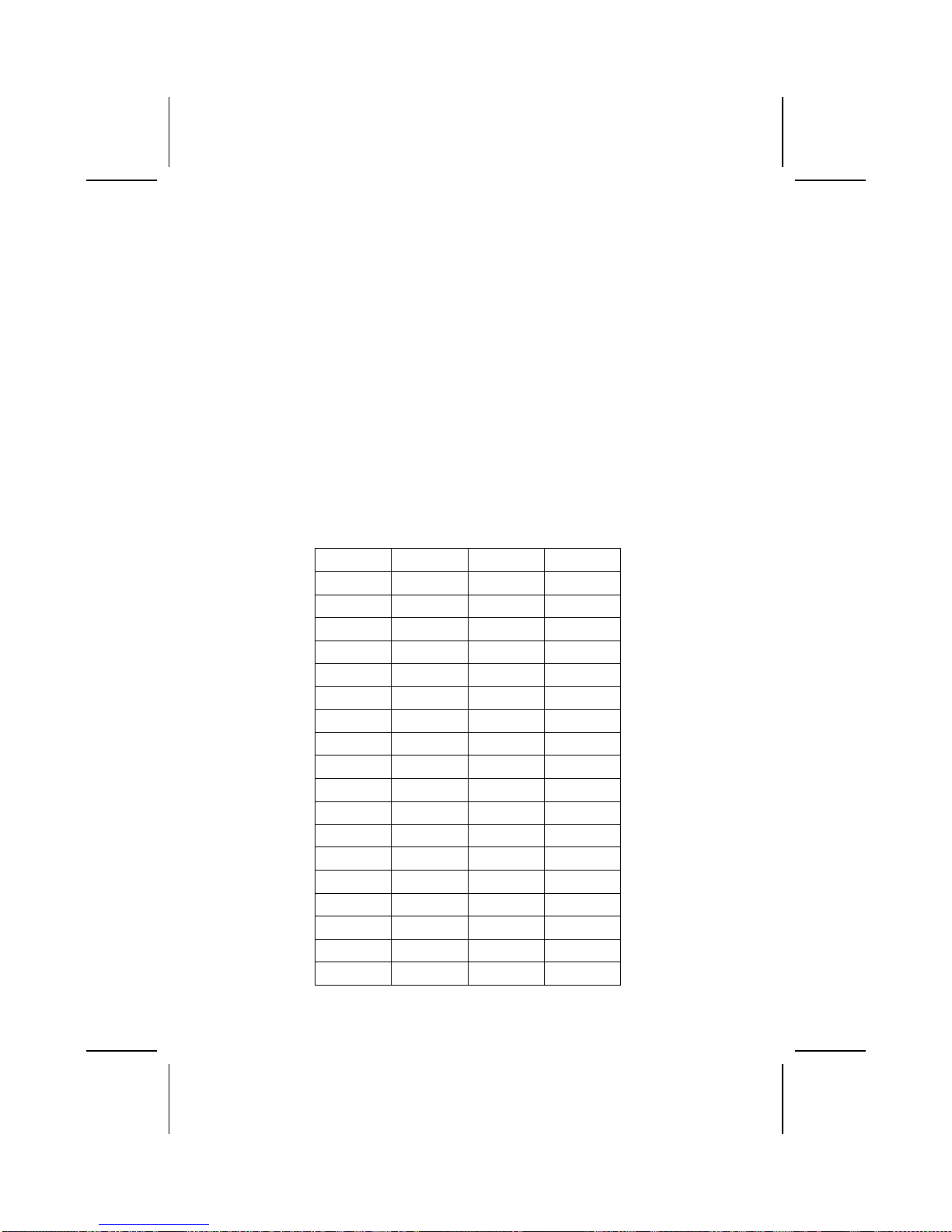
JP4 - The CPU voltage is defined according to the VID table. VID4 and VID 3
are derived from the CPU only and cannot be changed. While VID0 ~ VID2
can be changed manually by setting the jumper 4 to adjust the CPU voltage.
However, this is not recommended. If you want to overclock, you might need
to increase the CPU voltage.
• Auto – Set the CPU voltage according to its default setting. Short
pin numbers 1-2, 4-5, 7-8.
• Manual – Set the CPU voltage manually. Open all pins of jumper
4 and set the pin as follow: Where VID0 ~ VID2 are pin num-
bers 2-3, 5-6, 8-9 respectively of jumper 4. Thus, VID0 ~ VID2
will be equal to “0” by shorting pin numbers 2-3, 5-6, 8-9 or “1”
by opening pin numbers 2-3, 5-6, 8-9.
VID4 and VID3 depend on the CPU.
VID [4:0] Vcore (V) VID [4:0] Vcore (V)
00000 1.850 10000 1.450
00001 1.825 10001 1.425
00010 1.800 10010 1.400
00011 1.775 10011 1.375
00100 1.750 10100 1.350
00101 1.725 10101 1.325
00110 1.700 10110 1.300
00111 1.675 10111 1.275
01000 1.650 11000 1.250
01001 1.625 11001 1.225
01010 1.600 11010 1.200
01001 1.625 11001 1.225
01010 1.600 11010 1.200
01011 1.575 11011 1.175
01100 1.550 11100 1.150
01101 1.525 11101 1.125
01110 1.500 11110 1.100
01111 1.475 11111 No CPU
10

C
Co
on
nn
ne
ec
ct
ti
in
ng
g
C
Ca
as
se
e
C
Co
om
mp
po
on
ne
en
nt
ts
s
After you have installed the mainboard into a case, you can begin connecting
the mainboard components. Refer to the following:
1. Connect the case
power supply
connector to ATX1.
2. Connect the CPU
cooling fan cable to
CPUFAN.
3. Connect the case
cooling fan connector
to CASFAN.
4. Connect the case
switches and indicator
to PANEL1.
5. Connect the case
LED cable to J3 or
SJ1.
ATX1: ATX 20-pin Power Connector
Pin Signal Name Pin Signal Name
1 +3.3V 11 +3.3V
2 +3.3V 12 -12V
3 Ground 13 Ground
4 +5V 14 PS ON#
5 Ground 15 Ground
6 +5V 16 Ground
7 Ground 17 Ground
8 PWRGD 18 +5V
9 +5VSB 19 +5V
10 +12V 20 +5V
CPUFAN1/CASFAN1: FAN Power Connectors
Pin Signal Name Function
1 GND System Ground
2 +12V Power +12V
3 Sense Sensor
11
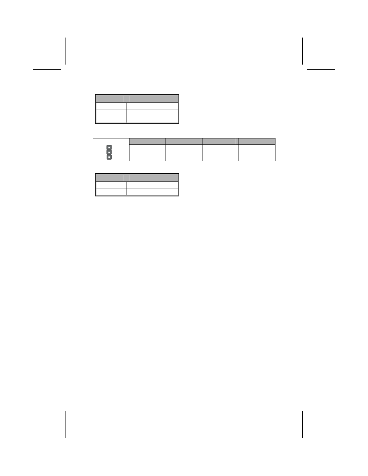
SJI: Single-color LED header
Pin Signal Name
1 ACPI LED
2 ACPI LED
3 5VSB
ACPI LED function:
S0 S1 S3 S4/S5
SJ1
1
Light Blinking Blinking Dark
J3: Single-color LED header
Pin Signal Name
1 LED+
2 Ground
12

Front Panel Connector
The front panel connector (PANEL1) provides a standard set of switch and
LED connectors commonly found on ATX or micro-ATX cases. Refer to the
table below for information:
PANEL1
Pin Signal Function Pin Signal Function
1 HD_LED_P Hard disk LED
(positive) 2 FP PWR/SLP MSG LED [dual color
or single color (+)]
3 HD_LED_N Hard disk active LED
(negative) 4 FP PWR/SLP MSG LED [dual color
or single color (-)]
5 RST_SW_N Reset Switch 6 PWR_SW_P Power Switch
7 RST_SW_P Reset Switch 8 PWR_SW_N Power Switch
9 RSVD Reserved 10 NC No pin
Hard Drive Activity LED
Connecting pins 1 and 3 to a front panel mounted LED provides visual indica-
tion that data is being read from or written to the hard drive. For the LED to
function properly, an IDE drive should be connected to the onboard IDE inter-
face. The LED will also show activity for devices connected to the SCSI (hard
drive activity LED) connector.
Power / Sleep / Message Waiting LED
Connecting pins 2 and 4 to a single- or dual-color, front panel mounted LED
provides power on/off, sleep, and message waiting indication.
Reset Switch
Supporting the reset function requires connecting pins 5 and 7 to a momen-
tary-contact switch that is normally open. When the switch is closed, the board
resets and runs POST.
Power Switch
Supporting the power on/off function requires connecting pins 6 and 8 to a
momentary-contact switch that is normally open. The switch should maintain
contact for at least 50 ms to signal the power supply to switch on or off. The
time requirement is due to internal debounce circuitry. After receiving a power
on/off signal, at least two seconds elapses before the power supply recog-
nizes another on/off signal.
13

I
In
ns
st
ta
al
ll
li
in
ng
g
H
Ha
ar
rd
dw
wa
ar
re
e
Installing the Processor
Caution: When installing a CPU heatsink and cooling fan make sure that
you DO NOT scratch the mainboard or any of the surface-mount resistors
with the clip of the cooling fan. If the clip of the cooling fan scrapes
across the mainboard, you may cause serious damage to the mainboard
or its components.
On most mainboards, there are small surface-mount resistors near the
processor socket, which may be damaged if the cooling fan is carelessly
installed.
Avoid using cooling fans with sharp edges on the fan casing and the
clips. Also, install the cooling fan in a well-lit work area so that you can
clearly see the mainboard and processor socket.
Before installing the Processor
This mainboard automatically determines the CPU clock frequency and sys-
tem bus frequency for the processor. You may be able to change these
settings by making changes to jumpers on the mainboard, or changing the
settings in the system Setup Utility. We strongly recommend that you do not
overclock processors or other components to run faster than their rated speed.
Warning: Overclocking components can adversely affect the reliability of
the system and introduce errors into your system. Overclocking can per-
manently damage the mainboard by generating excess heat in
components that are run beyond the rated limits.
This mainboard has a Socket 478 processor socket. When choosing a proc-
essor, consider the performance requirements of the system. Performance is
based on the processor design, the clock speed and system bus frequency of
the processor, and the quantity of internal cache memory and external cache
memory.
14

CPU Installation Procedure
The following illustration shows CPU installation components:
Note: The pin-1 corner is marked with an arrow
Follow these instructions to install the Retention Module and CPU:
1. Remove the existing retention module (if applicable).
2. Position the backplate
against the underside of
the mainboard; secure
the 4 screws firmly on
the retention module.
Note: Do not over tighten
the screws.
3. Install your CPU. Pull up
the lever away from the
socket and lift up to 90-
degree angle.
15

4. Locate the CPU cut
edge (the corner with the
pinhole noticeably miss-
ing). Align and insert the
CPU correctly.
5. Press the lever down.
6. Apply thermal grease on top of the CPU.
7. Put the CPU Fan down
on the retention module
and snap the four reten-
tion legs of the cooling
fan into place.
8. Flip the levers over to lock the heat sink in place.
9. Connect the CPU Cool-
ing Fan power cable to
the CPUFAN1 connec-
tor. This completes the
installation.
Notes: • To achieve better airflow rates and heat dissipation, we suggest that
you use a high quality fan with 4800 rpm at least.
• CPU fan and heatsink installation procedures may vary with the type of
CPU fan/heatsink supplied. The form and size of fan/heatsink may also
vary.
16
Table of contents
Other ECS Motherboard manuals


