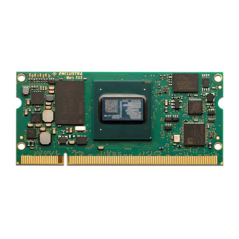
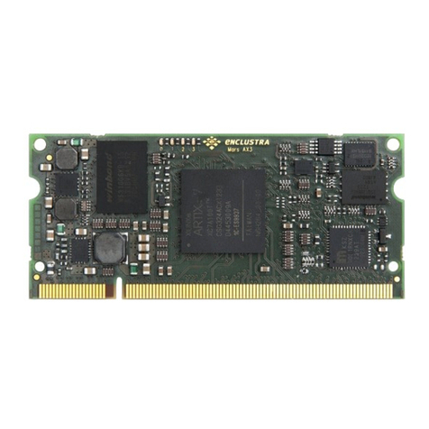
Enclustra Mars ZX3 User manual

Mars ZX3 SoC Module
User Manual
Purpose
The purpose of this document is to present the characteristics of Mars ZX3 SoC module to the user, and to
provide the user with a comprehensive guide to understanding and using the Mars ZX3 SoC module.
Summary
This document first gives an overview of the Mars ZX3 SoC module followed by a detailed description of its
features and configuration options. In addition, references to other useful documents are included.
Product Information Number Name
Product MA-ZX3 Mars ZX3 SoC Module
Document Information Reference Version Date
Reference / Version / Date D-0000-424-004 05 21.08.2018
Approval Information Name Position Date
Written by DIUN, GKOE Design Engineer 18.04.2016
Verified by GLAC Technical Expert 27.04.2016
Approved by RPAU Quality Manager 21.08.2018
Enclustra GmbH – Räffelstrasse 28 – CH-8045 Zürich – Switzerland
Phone +41 43 343 39 43 – www.enclustra.com

Copyright Reminder
Copyright 2018 by Enclustra GmbH, Switzerland. All rights are reserved.
Unauthorized duplication of this document, in whole or in part, by any means is prohibited without the prior
written permission of Enclustra GmbH, Switzerland.
Although Enclustra GmbH believes that the information included in this publication is correct as of the date
of publication, Enclustra GmbH reserves the right to make changes at any time without notice.
All information in this document is strictly confidential and may only be published by Enclustra GmbH,
Switzerland.
All referenced trademarks are the property of their respective owners.
Document History
Version Date Author Comment
05 21.08.2018 DIUN Minor corrections and style updates
04 04.05.2017 DIUN Updated EEPROM map, block diagram and footprint information
03 27.12.2016 DIUN Added tool support information and NAND flash programming in-
formation
02 11.08.2016 DIUN Minor updates and clarifications
01 03.05.2016 DIUN Version 01
D-0000-424-004 2 / 48 Version 05, 21.08.2018

Table of Contents
1 Overview 5
1.1 General ................................................... 5
1.1.1 Introduction ................................................ 5
1.1.2 Warranty .................................................. 5
1.1.3 RoHS .................................................... 5
1.1.4 DisposalandWEEE ............................................ 5
1.1.5 Safety Recommendations and Warnings . . . . . . . . . . . . . . . . . . . . . . . . . . . . . . . . 5
1.1.6 ElectrostaticDischarge .......................................... 6
1.1.7 Electromagnetic Compatibility . . . . . . . . . . . . . . . . . . . . . . . . . . . . . . . . . . . . . . 6
1.2 Features................................................... 6
1.3 Deliverables ................................................ 6
1.4 Accessories................................................. 7
1.4.1 ReferenceDesign ............................................. 7
1.4.2 EnclustraBuildEnvironment ....................................... 7
1.4.3 MarsPM3BaseBoard........................................... 7
1.4.4 MarsEB1BaseBoard ........................................... 7
1.5 XilinxToolSupport ............................................ 8
2 Module Description 9
2.1 BlockDiagram............................................... 9
2.2 Module Configuration and Product Codes . . . . . . . . . . . . . . . . . . . . . . . . . . . . . . . 9
2.3 Article Numbers and Article Codes . . . . . . . . . . . . . . . . . . . . . . . . . . . . . . . . . . . 10
2.4 TopandBottomViews .......................................... 12
2.4.1 TopView .................................................. 12
2.4.2 BottomView................................................ 12
2.5 Top and Bottom Assembly Drawings . . . . . . . . . . . . . . . . . . . . . . . . . . . . . . . . . . 13
2.5.1 TopAssemblyDrawing .......................................... 13
2.5.2 BottomAssemblyDrawing........................................ 13
2.6 ModuleFootprint ............................................. 13
2.7 MechanicalData.............................................. 14
2.8 ModuleConnector ............................................ 14
2.9 UserI/O................................................... 15
2.9.1 Pinout.................................................... 15
2.9.2 DifferentialI/Os .............................................. 16
2.9.3 I/OBanks.................................................. 16
2.9.4 VREFUsage................................................. 17
2.9.5 VCC_IOUsage ............................................... 17
2.9.6 SignalTerminations ............................................ 18
2.9.7 MultiplexedI/O(MIO)Pins........................................ 19
2.9.8 AnalogInputs ............................................... 20
2.10 Power.................................................... 20
2.10.1 PowerGenerationOverview ....................................... 20
2.10.2 PowerEnable/PowerGood........................................ 21
2.10.3 VoltageSupplyInputs........................................... 21
2.10.4 VoltageSupplyOutputs ......................................... 22
2.10.5 PowerConsumption............................................ 22
2.10.6 HeatDissipation.............................................. 23
2.11 ClockGeneration ............................................. 23
2.12 Reset .................................................... 24
2.13 LEDs..................................................... 24
2.14 DDR3SDRAM ............................................... 24
2.14.1 DDR3SDRAMType ............................................ 25
2.14.2 SignalDescription............................................. 25
2.14.3 Termination................................................. 25
D-0000-424-004 3 / 48 Version 05, 21.08.2018

2.14.4 Parameters................................................. 25
2.14.5 DDR3LowVoltageOperation ...................................... 26
2.15 QSPIFlash ................................................. 26
2.15.1 QSPIFlashType .............................................. 27
2.15.2 SignalDescription............................................. 27
2.15.3 Configuration ............................................... 27
2.16 NANDFlash ................................................ 28
2.16.1 NANDFlashType ............................................. 28
2.16.2 SignalDescription............................................. 28
2.16.3 Parameters................................................. 28
2.17 SDCard................................................... 29
2.18 GigabitEthernet.............................................. 29
2.18.1 EthernetPHYType............................................. 29
2.18.2 SignalDescription............................................. 30
2.18.3 ExternalConnectivity ........................................... 30
2.18.4 MDIOAddress............................................... 30
2.18.5 PHYConfiguration............................................. 31
2.19 USB2.0 ................................................... 31
2.19.1 USBPHYType ............................................... 31
2.19.2 SignalDescription............................................. 31
2.20 Real-TimeClock(RTC)........................................... 31
2.20.1 RTCType .................................................. 32
2.21 SecureEEPROM .............................................. 32
2.21.1 EEPROMType ............................................... 32
2.22 RevisionDetection............................................. 32
3 Device Configuration 33
3.1 ConfigurationSignals........................................... 33
3.2 Pull-UpDuringConfiguration ...................................... 34
3.3 BootMode................................................. 34
3.3.1 JTAGBootMode.............................................. 35
3.3.2 NANDFlashBootMode ......................................... 35
3.4 JTAG..................................................... 35
3.4.1 JTAGonModuleConnector ....................................... 36
3.4.2 ExternalConnectivity ........................................... 36
3.5 QSPIBootMode.............................................. 36
3.6 SDCardBootMode............................................ 36
3.7 QSPI Flash Programming via JTAG . . . . . . . . . . . . . . . . . . . . . . . . . . . . . . . . . . . 36
3.8 QSPI Flash Programming from an External SPI Master . . . . . . . . . . . . . . . . . . . . . . . . 37
3.9 NANDFlashProgramming........................................ 37
3.10 FPGA and QSPI Flash Programming using Xilinx Impact . . . . . . . . . . . . . . . . . . . . . . . 38
3.11 Enclustra Module Configuration Tool . . . . . . . . . . . . . . . . . . . . . . . . . . . . . . . . . . 38
4 I2C Communication 39
4.1 Overview .................................................. 39
4.2 SignalDescription............................................. 39
4.3 I2CAddressMap ............................................. 40
4.4 SecureEEPROM .............................................. 40
4.4.1 MemoryMap ............................................... 40
5 Operating Conditions 43
5.1 AbsoluteMaximumRatings ....................................... 43
5.2 Recommended Operating Conditions . . . . . . . . . . . . . . . . . . . . . . . . . . . . . . . . . 44
6 Ordering and Support 45
6.1 Ordering .................................................. 45
6.2 Support................................................... 45
D-0000-424-004 4 / 48 Version 05, 21.08.2018

1 Overview
1.1 General
1.1.1 Introduction
The Mars ZX3 SoC module combines the Xilinx Zynq®-7020 All Programmable SoC (System-on-Chip) de-
vice with fast DDR3 SDRAM, NAND flash, quad SPI flash, a Gigabit Ethernet PHY, USB 2.0 On-The-Go PHY
and a real-time clock, forming a complete and powerful embedded processing system.
The SO-DIMM form factor allows space-saving hardware designs and quick and simple integration of the
module into the target application.
The use of the Mars ZX3 SoC module, in contrast to building a custom SoC hardware, significantly reduces
development effort and redesign risk and improves time-to-market for the embedded system.
Together with Mars base boards, the Mars ZX3 SoC module allows the user to quickly build a system pro-
totype and start with application development.
The Enclustra Build Environment [15] is available for the Mars ZX3 SoC module. This build system allows
the user to quickly set up and run Linux on any Enclustra SoC module. It allows the user to choose the
desired target and download all the required binaries, such as bitstream and FSBL (First Stage Boot Loader).
It downloads and compiles all required software, such as U-Boot, Linux, and BusyBox based root file system.
1.1.2 Warranty
Please refer to the General Business Conditions, available on the Enclustra website [1].
1.1.3 RoHS
The Mars ZX3 SoC module is designed and produced according to the Restriction of Hazardous Substances
(RoHS) Directive (2011/65/EC).
1.1.4 Disposal and WEEE
The Mars ZX3 SoC module must be properly disposed of at the end of its life.
The Waste Electrical and Electronic Equipment (WEEE) Directive (2002/96/EC) is not applicable for the Mars
ZX3 SoC module.
1.1.5 Safety Recommendations and Warnings
Mars modules are not designed to be “ready for operation” for the end-user. These can only be used in
combination with suitable base boards. Proper configuration of the hardware before usage is required.
Ensure that the power supply is disconnected from the board before inserting or removing the Mars ZX3
SoC module, connecting interfaces, replacing SD cards and batteries, or connecting jumpers.
Touching the capacitors of the DC-DC converters can lead to voltage peaks and permanent damage; over-
voltage on power or signal lines can also cause permanent damage to the module.
D-0000-424-004 5 / 48 Version 05, 21.08.2018

Warning!
Use the Mars ZX3 SoC module only with base boards designed for the Enclustra Mars module family.
Inserting the Mars ZX3 SoC module into a SO-DIMM connector designed for memory (e.g. a computer
main board) may damage the module and the carrier board.
1.1.6 Electrostatic Discharge
Electronic boards are sensitive to electrostatic discharge (ESD). Please ensure that the product is handled
with care and only in an ESD-protected environment.
1.1.7 Electromagnetic Compatibility
The Mars ZX3 SoC module is a Class A product and is not intended for use in domestic environments. The
product may cause electromagnetic interference, for which appropriate measures must be taken.
1.2 Features
•Xilinx Zynq®-7020 All Programmable SoC, CLG484 package
•Dual ARM® Cortex™-A9 MPCore™with CoreSight™ and NEON™ extension
•Xilinx Artix-7 28 nm FPGA fabric
•108 user I/Os up to 3.3 V
•12 ARM peripheral I/Os (SPI, SDIO, CAN, I2C, UART) shared with FPGA I/Os
•96 FPGA I/Os (single-ended, differential or analog)
•Up to 1 GB DDR3 SDRAM
•512 MB NAND flash
•64 MB quad SPI flash
•Gigabit Ethernet
•USB 2.0 On-The-Go (OTG)
•Real-time clock
•SO-DIMM form factor (30 ×67.6 mm, 200 pins)
•The module can be operated using a single 3.3 V supply voltage
1.3 Deliverables
•Mars ZX3 SoC module
•Mars ZX3 SoC module documentation, available via download:
•Mars ZX3 SoC Module User Manual (this document)
•Mars ZX3 SoC Module Reference Design [2]
•Mars ZX3 SoC Module IO Net Length Excel Sheet [3]
•Mars ZX3 SoC Module FPGA Pinout Excel Sheet [4]
•Mars ZX3 SoC Module User Schematics (PDF) [5]
•Mars ZX3 SoC Module Known Issues and Changes [6]
•Mars ZX3 SoC Module Footprint (Altium, Eagle, Orcad and PADS) [7]
•Mars ZX3 SoC Module 3D Model (PDF) [8]
•Mars ZX3 SoC Module STEP 3D Model [9]
•Module Pin Connection Guidelines [10]
•Mars Master Pinout [11]
•Enclustra Modules Heat Sink Application Note [17]
•Enclustra Build Environment [15] (Linux build environment; refer to Section 1.4.2 for details)
D-0000-424-004 6 / 48 Version 05, 21.08.2018

1.4 Accessories
1.4.1 Reference Design
The Mars ZX3 SoC module reference design features an example configuration for the Zynq-7000 SoC de-
vice, together with an example top level HDL file for the user logic.
A number of software applications are available for the reference design, that show how to initialize the
peripheral controllers and how to access the external devices. Pre-compiled binaries are included in the
archive, so that the user can easily check that the hardware is functional.
The reference design can be downloaded from the Enclustra download page [2].
1.4.2 Enclustra Build Environment
The Enclustra Build Environment [15] enables the user to quickly set up and run Linux on any Enclustra SoC
module. It allows the user to choose the desired target, and download all the required binaries, such as
bitstream and FSBL. It downloads and compiles all required software, such as U-Boot, Linux, and BusyBox
based root file system.
The Enclustra Build Environment features a graphical user interface (GUI) and a command line interface (CLI)
that facilitates the automatic build flow.
1.4.3 Mars PM3 Base Board
•Mars 200-pin SO-DIMM socket
•FMC LPC (Low Pin Count) connector (72 I/Os)
•40-pin GPIO connector (optional, shared with FMC I/Os)
•RJ45 Gigabit Ethernet connector
•Mini HDMI connector for PCIe and LVDS applications (module dependent)
•Cypress FX3 USB 3.0 device controller (16-bit Slave-FIFO interface or 32-bit Slave-FIFO interface shared
with FMC I/Os)
•USB 3.0 B device connector
•USB 2.0 A host connector
•Micro USB 2.0 B device connector with FTDI USB device controller
•Battery holder for the real-time clock
•microSD card holder
•Fan connector, various switches and LEDs
•Single 12 V DC supply voltage or USB bus-powered (with restrictions)
•Form factor: 100 ×72 mm (pico-ITX)
Please note that the available features depend on the equipped Mars module type.
1.4.4 Mars EB1 Base Board
•Mars 200-pin SO-DIMM socket
•2×Mini Camera Link connectors (requires FPGA support)
•HDMI 1.3 connector (requires FPGA support)
•40-pin GPIO connector (Anios)
•3×12-pin GPIO connector (two of the connectors with Pmod™ compatible pinout)
•RJ45 Ethernet connector
•USB 2.0 A host connector
•Micro USB 2.0 device connector (shared)
•FTDI USB 2.0 device controller with micro USB device connector
•microSD card holder
•Various switches and LEDs
•Integrated Xilinx compatible JTAG adapter
D-0000-424-004 7 / 48 Version 05, 21.08.2018

•Single 12 V DC supply voltage or USB bus-powered (with restrictions)
•Form factor: 120 ×80 mm
Please note that the available features depend on the equipped Mars module type.
1.5 Xilinx Tool Support
The SoC devices equipped on the Mars ZX3 SoC module are supported by the Vivado HL WebPACK Edition
software, which is available free of charge. Please contact Xilinx for further information.
D-0000-424-004 8 / 48 Version 05, 21.08.2018

2 Module Description
2.1 Block Diagram
Figure 1: Hardware Block Diagram
The main component of the Mars ZX3 SoC module is the Xilinx Zynq-7000 SoC device. Most of its I/O pins
are connected to the Mars module connector, making 108 user I/Os available to the user.
The SoC device can boot from the on-board QSPI flash, NAND flash or from an external SD card. For de-
velopment purposes, a JTAG interface is connected to Mars module connector.
The available standard configurations include 512 MB NAND flash, a 64 MB quad SPI flash and 512 MB or 1
GB DDR3 SDRAM.
Further, the module is equipped with a Gigabit Ethernet PHY and a USB 2.0 OTG PHY, making it ideal for
communication applications.
A real-time clock is available on the module and is connected to the global I2C bus.
On-board clock generation is based on a 33.33 MHz crystal oscillator.
The module can be operated using a single input supply of 3.3 V DC. All other necessary supply voltages are
generated on-board. Some of these voltages are available on the Mars module connector to supply circuits
on the base board.
Four LEDs are connected to the SoC pins for status signaling.
2.2 Module Configuration and Product Codes
Table 1 describes the available standard module configurations. Custom configurations are available; please
contact Enclustra for further information.
D-0000-424-004 9 / 48 Version 05, 21.08.2018

Product Code SoC DDR3/DDR3L SDRAM Temperature Range
MA-ZX3-20-1C-D9 XC7Z020-1CLG484C 512 MB 0 to +70◦C
MA-ZX3-20-2I-D10 XC7Z020-2CLG484I 1024 MB -40 to +85◦C
Table 1: Standard Module Configurations
The product code indicates the module type and main features. Figure 2 describes the fields within the
product code.
Figure 2: Product Code Fields
Please note that for the first revision modules or early access modules, the product code may not respect
entirely this naming convention. Please contact Enclustra for details on this aspect.
2.3 Article Numbers and Article Codes
Every module is uniquely labeled, showing the article number and serial number. An example is presented
in Figure 3.
Figure 3: Module Label
The correspondence between article number and article code is shown in Table 2. The article code repre-
sents the product code, followed by the revision; the R suffix and number represent the revision number.
The revision changes and product known issues are described in the Mars ZX3 SoC Module Known Issues
and Changes document [6].
D-0000-424-004 10 / 48 Version 05, 21.08.2018

Article Number Article Code
EN100021 MA-ZX3-20-1C-D9-R2
EN100022 MA-ZX3-20-2I-D10-R2
EN100079 MA-ZX3-20-2I-D10-R3
EN100080 MA-ZX3-20-1C-D9-R3
EN100915 MA-ZX3-20-1C-D9-R4
EN100916 MA-ZX3-20-2I-D10-R4
EN101311 MA-ZX3-20-1C-D9-R5
EN101312 MA-ZX3-20-2I-D10-R5
EN101493 MA-ZX3-20-1C-D9-R6
EN101494 MA-ZX3-20-2I-D10-R6
EN101556 MA-ZX3-20-1C-D9-R6.1
EN101557 MA-ZX3-20-2I-D10-R6.1
Table 2: Article Numbers and Article Codes
D-0000-424-004 11 / 48 Version 05, 21.08.2018

2.5 Top and Bottom Assembly Drawings
2.5.1 Top Assembly Drawing
Figure 6: Module Top Assembly Drawing
2.5.2 Bottom Assembly Drawing
Figure 7: Module Bottom Assembly Drawing
Please note that depending on the hardware revision and configuration, the module may look slightly dif-
ferent than shown in this document.
2.6 Module Footprint
Figure 8 shows the dimensions of the module footprint on the base board.
The maximum component height under the module is dependent on the connector type - refer to Section
2.8 for detailed connector information.
D-0000-424-004 13 / 48 Version 05, 21.08.2018

Figure 8: Module Footprint - Top View
The footprint of the module connector is available for different PCB design tools (Altium, Eagle, Orcad, PADS)
[7].
2.7 Mechanical Data
Table 3 describes the mechanical characteristics of the Mars ZX3 SoC module. A 3D model (PDF) and a STEP
3D model are available [8], [9].
Symbol Value
Size 67.6 ×30 mm
Component height top 2.0 mm
Component height bottom 1.2 mm
Weight 9 g
Table 3: Mechanical Data
2.8 Module Connector
The Mars ZX3 SoC module fits into a 200-pin DDR2 SO-DIMM (1.8 V) socket. Up to four M2 screws may be
used to mechanically fasten the module to the base board. Do not use excessive force to tighten the screws,
as this could damage the module.
The pinout of the module connector is found in the Mars Master Pinout Excel Sheet [11]. The connector to
be mounted on the base board is available in different heights. Some examples are presented in Table 4.
Please refer to the connector datasheet for more information.
D-0000-424-004 14 / 48 Version 05, 21.08.2018

Height Type Description Max component height under the module
4.0 mm TE 292406-4 DDR2-SODIMM, 1.8 V 0 mm
5.2 mm TE 1565917-4 DDR2-SODIMM, 1.8 V 1 mm
6.5 mm TE 5-1746530-4 DDR2-SODIMM, 1.8 V 2 mm
8.0 mm TE 1827341-4 DDR2-SODIMM, 1.8 V 4 mm
Table 4: Module Connector Types
2.9 User I/O
2.9.1 Pinout
Information on the Mars ZX3 SoC module pinout can be found in the Enclustra Mars Master Pinout [11], and
in the additional document Enclustra Module Pin Connection Guidelines [10].
The naming convention for the user I/Os is:
IO_B<BANK>_L<PAIR><_SPECIAL_FUNCTION>_<PACKAGE_PIN>_<POLARITY>.
For example, IO_B35_L1_AD0_F16_P is located on pin F16 of I/O bank 35, pair 1, it is an XADC auxiliary analog
input capable pin and it has positive polarity, when used in a differential pair.
For the signal lines shared between Programmable Logic (PL) and Processing System (PS), the naming con-
vention is:
IO_<MIO_PIN>_B<BANK>_L<PAIR>_<PACKAGE_PIN>
For example, IO_MIO44_B33_L16_U17 is connected to FPGA pin U17 and in parallel to the PS MIO pin 44.
Please note that for the shared pins only one of the driving pins (FPGA pin, MIO pin) may be active.
The multi-region clock capable pins are marked with “MRCC”, while the single region clock capable pins are
marked with “SRCC” in the signal name. For details on their function and usage, please refer to the Xilinx
documentation.
Table 5 includes information related to the total number of I/Os available in each I/O bank and possible
limitations.
Signal Name Signals Pairs Differential Single-ended I/O Bank
IO_<MIO_PIN>_B33_<...> 12 6 In/Out In/Out 33
IO_B34_<...> 48 24 In/Out In/Out 34
IO_B35_<...> 48 24 In/Out In/Out 35
Total 108 54 - - -
Table 5: User I/Os
Please note that for the 7 Series FPGAs there are restrictions on the VCCO voltage when using LVDS I/Os;
refer to Xilinx AR# 43989 for details.
D-0000-424-004 15 / 48 Version 05, 21.08.2018

2.9.2 Differential I/Os
When using differential pairs, a differential impedance of 100 Ωmust be matched on the base board, and
the two nets of a differential pair must have the same length.
The information regarding the length of the signal lines from the SoC device to the module connector is
available in Mars ZX3 SoC Module IO Net Length Excel Sheet [3]. This enables the user to match the total
length of the differential pairs on the base board if required by the application.
2.9.3 I/O Banks
Table 6 describes the main attributes of the FPGA and PS I/O banks, and indicates which peripherals are
connected to each I/O bank. All I/O pins within a particular I/O bank must use the same I/O (VCC_IO) and
reference (VREF) voltages.
Bank Connectivity VCC_IO VREF
Bank 0 Configuration User selectable -
VCC_CFG_PS_B13_B33
Bank 13 Ethernet PHY User selectable -
Most pins shared with MIO 16-27 VCC_CFG_PS_B13_B33
Bank 33 Module connector User selectable -
Most pins shared with MIO 40-51 VCC_CFG_PS_B13_B33
Bank 34 Module connector User selectable IO_B34_L6_VREF_M16_N
VCC_IO_B34 IO_B34_L19_VREF_P15_N
Bank 35 Module connector User selectable IO_B35_L6_VREF_F17_N
VCC_IO_B35 IO_B35_L19_VREF_H20_N
PS MIO0 QSPI and NAND flash User selectable1
-
VCC_CFG_PS_B13_B33
PS MIO1 Ethernet PHY, USB PHY, User selectable 0.9 V
Module connector VCC_CFG_PS_B13_B332
PS DDR DDR3 SDRAM User selectable3
0.5 ×VREF_DDR3L
VCC_DDR3L
Table 6: I/O Banks
2 3
1For modules of revision 4 or older, the MIO0 bank voltage is tied to 3.3 V.
2On modules of revision 4 or older, the name of this voltage supply signal is: VCC_CFG_MIO1_B13_B33.
3The DDR3 SDRAM supports voltages of 1.5 or 1.35 V. Please refer to Section 2.14 for details.
D-0000-424-004 16 / 48 Version 05, 21.08.2018

Warning!
Some of the I/Os are connected to MIO pins and to user logic I/Os in parallel - make sure that at
least one of the two pins is configured to high impedance, and that pull-up or pull-down resistors are
disabled on both if they are not used.
Some of the system pins must be defined as input or high impedance. Please refer to the Mars ZX3
SoC module reference design for details [2].
2.9.4 VREF Usage
I/O standards referenced using VREF can be used on the Mars module connector. The reference voltage
has to be applied to all VREF pins of the respective I/O banks. If a bank is configured to use an I/O standard
that does not need a reference voltage, the VREF pins of this bank on the module connector are available
as user I/O pins.
The VREF pins are listed in the Mars Master Pinout Excel Sheet [11].
Warning!
Use only VREF voltages compliant with the equipped SoC device; any other voltages may damage the
equipped SoC device, as well as other devices on the Mars ZX3 SoC module.
Do not leave a VREF pin floating when the used I/O standard requires a reference voltage, as this may
damage the equipped SoC device, as well as other devices on the Mars ZX3 SoC module.
2.9.5 VCC_IO Usage
The VCC_IO voltages for the I/O banks located on the module connector are configurable by applying the
required voltage to the VCC_IO_B[x], respectively VCC_CFG_[x] pins. All VCC_IO_B[x] or VCC_CFG_[x] pins of
the same bank must be connected to the same voltage.
For compatibility with other Enclustra Mars base boards and modules, it is recommended to use a single
I/O voltage.
Signal Name SoC Pins Supported Voltages Connector Pins
VCC_CFG_PS_B13_B33 VCCO_13, VCCO_33,
VCC_MIO0, VCC_MIO1
1.8 V4, 2.5 V - 3.3 V5±5% 137, 146
VCC_IO_B34 VCCO_34 1.8 V - 3.3 V6±5% 53, 62, 73
VCC_IO_B35 VCCO_35 1.8 V - 3.3 V7±5% 82, 117, 126
Table 7: VCC_IO Pins
4 5 6 7
41.8 V support is only available for modules of revision 5 and newer. NAND flash is disabled when VCC_CFG_PS_B13_B33 is 1.8 V.
5The RGMII Ethernet interface is specified only up to 2.5 V on the MIO pins by Xilinx. Please refer to Section 2.18 for details.
6I/O bank 34 can run down to 1.2 V if I2C bus access from the PL is not required.
7I/O bank 35 can run down to 1.2 V, but the FPGA LEDs will be always on in this case.
D-0000-424-004 17 / 48 Version 05, 21.08.2018

Note that the CFGBVS_0 pin is set automatically to GND (if VCC_CFG_PS_B13_B33 is less than or equal to 1.8
V) or to VCCO (if VCC_CFG_PS_B13_B33 is 2.5 V or 3.3 V).
Warning!
Use only VCC_IO voltages compliant with the equipped SoC device; any other voltages may damage
the equipped SoC device, as well as other devices on the Mars ZX3 SoC module.
Do not leave a VCC_IO pin floating, as this may damage the equipped SoC device, as well as other
devices on the Mars ZX3 SoC module.
Warning!
Do not power the VCC_IO pins when PWR_GOOD and PWR_EN signals are not active. If the module
is not powered, you need to make sure that the VCC_IO voltages are disabled (for example, by using
a switch on the base board, which uses PWR_GOOD as enable signal). Figure 9 illustrates the VCC_IO
power requirements.
Figure 9: Power-Up Sequence - VCC_IO in Relation with PWR_GOOD and PWR_EN Signals
2.9.6 Signal Terminations
Differential Inputs
There are no external differential termination resistors on the Mars ZX3 SoC module for differential inputs.
Differential input pairs on the module connector may be terminated either by external termination resistors
on the base board (close to the module pins), or by the SoC device’s internal termination resistors.
Internal differential termination is available only for certain VCCO voltages; please refer to Xilinx AR# 43989
for details.
Single-Ended Outputs
There are no series termination resistors on the Mars ZX3 SoC module for single-ended outputs. If required,
series termination resistors may be equipped on the base board (close to the module pins).
D-0000-424-004 18 / 48 Version 05, 21.08.2018

2.9.7 Multiplexed I/O (MIO) Pins
Details on the MIO/EMIO terminology are available in the Zynq-7000 All Programmable SoC Technical Ref-
erence Manual [18].
Some of the MIO pins on the Mars ZX3 SoC module are connected to on-board peripherals, while others
are available as GPIOs; the suggested functions below are for reference only - always verify your MIO pinout
with the Xilinx device handbook.
Table 9 gives an overview over the MIO pin connections on the Mars ZX3 SoC module. Only the pins marked
with “user functionality” are available on the module connector.
The MIO pins 52-53 have an external multiplexer that allows the pins to be switched either to the Ethernet
MDIO interface, or to the on-board I2C bus; by default, MDIO is selected. In order to switch to I2C operation,
MIO15 must be pulled low. Please refer to Table 8 for signal assignments.
It is recommended to use EMIO pins for I2C access. However, in situations where Ethernet is not used or
when I2C access is needed before a bitstream is loaded into the FPGA, MIO pins 52-53 may be used for I2C.
MIO Pin Function
MIO15 MDIO select = 0 MDIO select = 1 (default)
MIO52 On-board I2C bus (I2C1.SCL) Ethernet PHY MDC
MIO53 On-board I2C bus (I2C1.SDA) Ethernet PHY MDIO
Table 8: Special MIO Pins
MIO Group Function Connection
0-14 QSPI and NAND flash QSPI/NAND flash
15 MDIO select I2C/MDIO multiplexer selection
16-27 Ethernet Gigabit Ethernet PHY
28-39 USB USB 2.0 OTG PHY
40-45 SD card/user functionality Module connector
46 UART RX8/user functionality Module connector
47 UART TX8/user functionality
48-51 User functionality Module connector
Gigabit Ethernet PHY/
52-53 Ethernet MDIO/I2C On-board I2C bus and module connector
via level shifter
Table 9: MIO Pins Connections Overview
8UART RX is an SoC input; UART TX is an SoC output.
D-0000-424-004 19 / 48 Version 05, 21.08.2018

2.9.8 Analog Inputs
The Zynq-7000 SoC devices provide a dual 12-bit ADC. The auxiliary analog inputs of the SoC device are
connected to the module connector; these I/Os have the abbreviation “AD” followed by the ADC channel in
the signal name.
The two dedicated ADC pins VP and VN are available on the module connector on pins 168 and 170
(FPGA_V_P/N). The ADC can also be used for internal voltage and temperature monitoring. For detailed
information, refer to the Xilinx 7 Series XADC User Guide [19].
The ADC lines are always used differentially; for single-ended applications, the *_N line must be connected
to GND.
Table 10 presents the ADC Parameters.
Parameter Value
VCC_ADC 1.8 V
GND_ADC 0 V (connected to GND via ferrite)
VREF_ADC 1.25 V
ADC Range 0-1 V
Sampling Rate per ADC 1 MSPS
Total number of channels 17 (1 dedicated channel, 16 auxiliary inputs)
Table 10: ADC Parameters
2.10 Power
2.10.1 Power Generation Overview
The Mars ZX3 SoC module uses a 3.3 - 5.0 V DC power input for generating the on-board supply voltages
(1.0 V, 1.35 V/1.5 V, 1.8 V). These internally-generated voltages are accessible on the module connector. In
addition, a separate 3.3 V power input is used to supply peripherals, such as the Ethernet PHY, QSPI flash,
oscillator, RTC, EEPROM and LEDs.
The Mars ZX3 SoC module can be powered using a single power supply. In this case, the two voltage supply
inputs VCC_MOD and VCC_3V3 must be connected together to a 3.3 V supply. Please refer to Section 2.10.3
for details on the voltage supply inputs.
Table 11 describes the power supplies generated on the module.
D-0000-424-004 20 / 48 Version 05, 21.08.2018
This manual suits for next models
15
Table of contents
Other Enclustra Control Unit manuals
Enclustra
Enclustra Mercury SA1 SoC Module User manual
Enclustra
Enclustra Mars ZX2 User manual
Enclustra
Enclustra Mercury+ XU8 SoC User manual
Enclustra
Enclustra Mercury+ KX2 User manual
Enclustra
Enclustra Mercury+ XU7 User manual
Enclustra
Enclustra Mercury+ XU8 User manual
Enclustra
Enclustra Mercury+ XU9 User manual
Enclustra
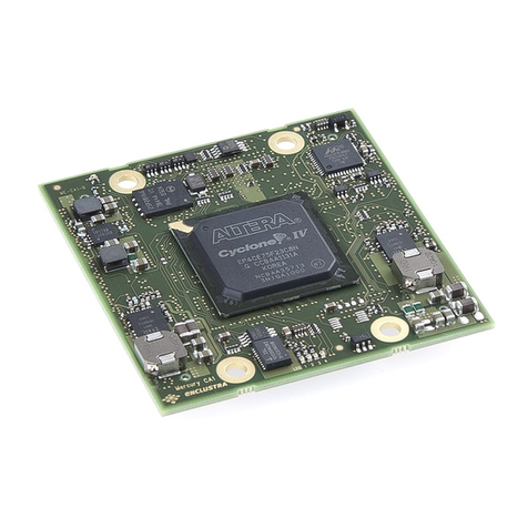
Enclustra Mercury CA1 User manual
Enclustra
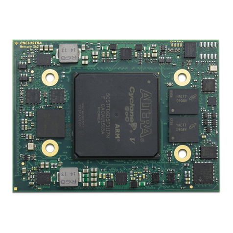
Enclustra Mercury+ SA2 User manual
Enclustra
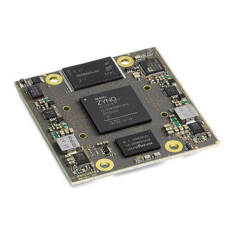
Enclustra Mercury ZX5 Series User manual

