FLY E195 User manual

E195 Service Menu
Version number: V1.0
Contents
1OVERVIEW E195..........................................................................................................................1
1.1ABOUT E195 PHONE.................................................................................................................1
1.2DISTRIBUTION OF THE MAINBOARD COMPONENTS....................................................................3
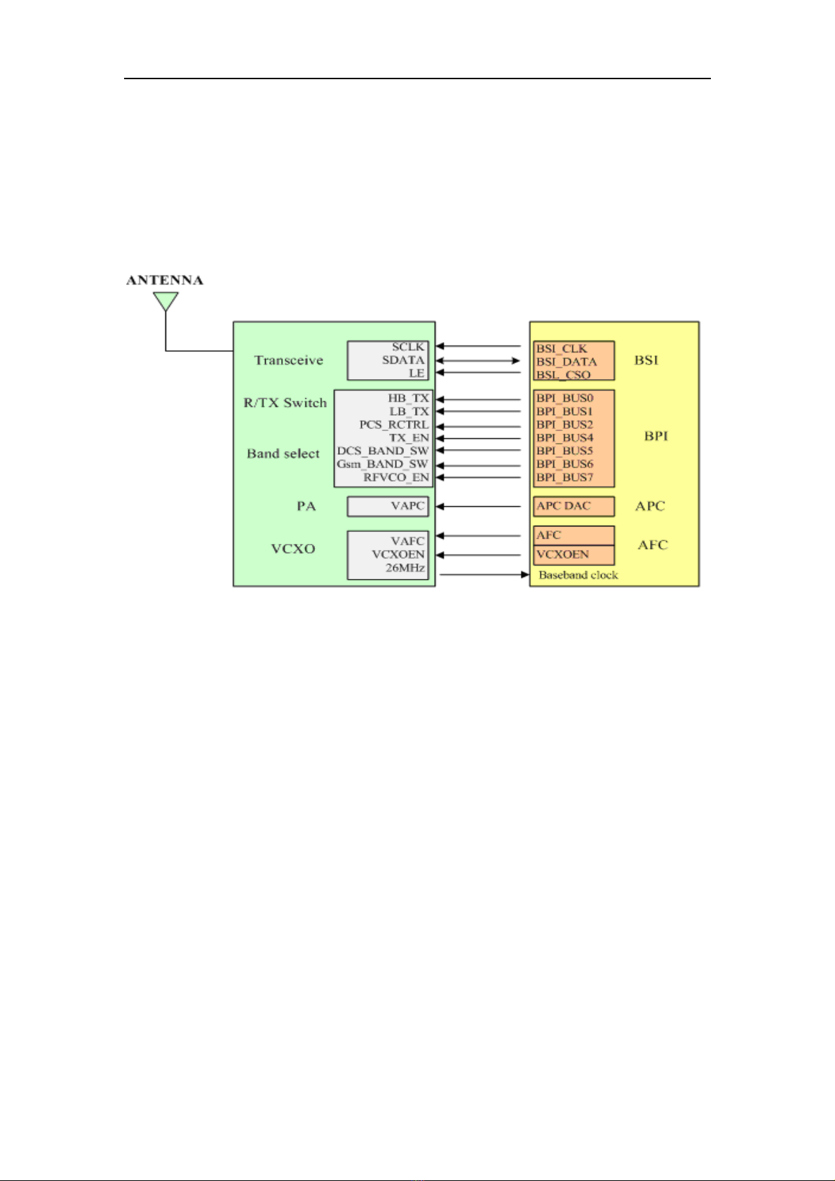
2RF....................................................................................................................................................5
2.1RF OVERVIEW ..........................................................................................................................5
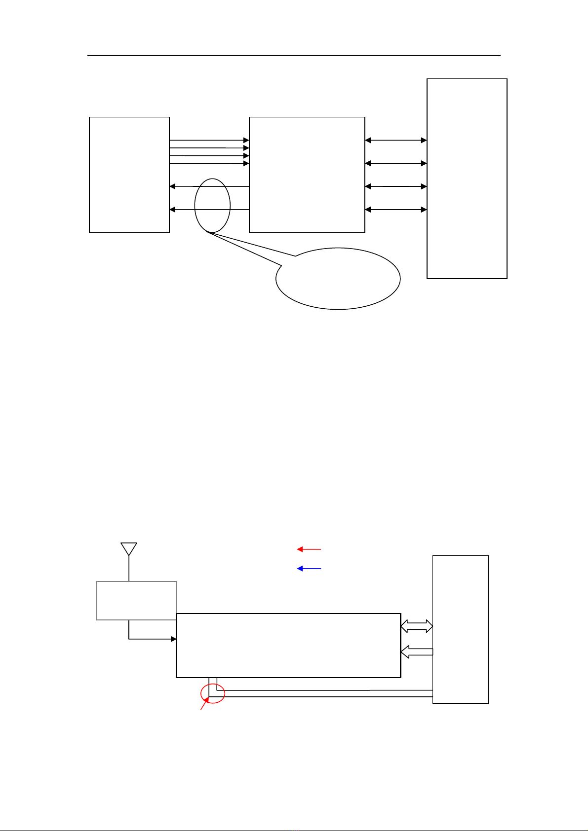
2.2TRANSMIT ................................................................................................................................5
2.3RECEIVE ...................................................................................................................................6
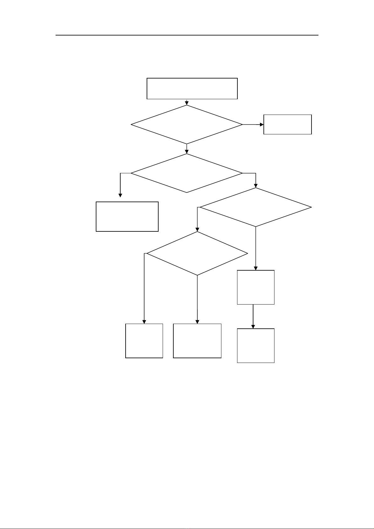
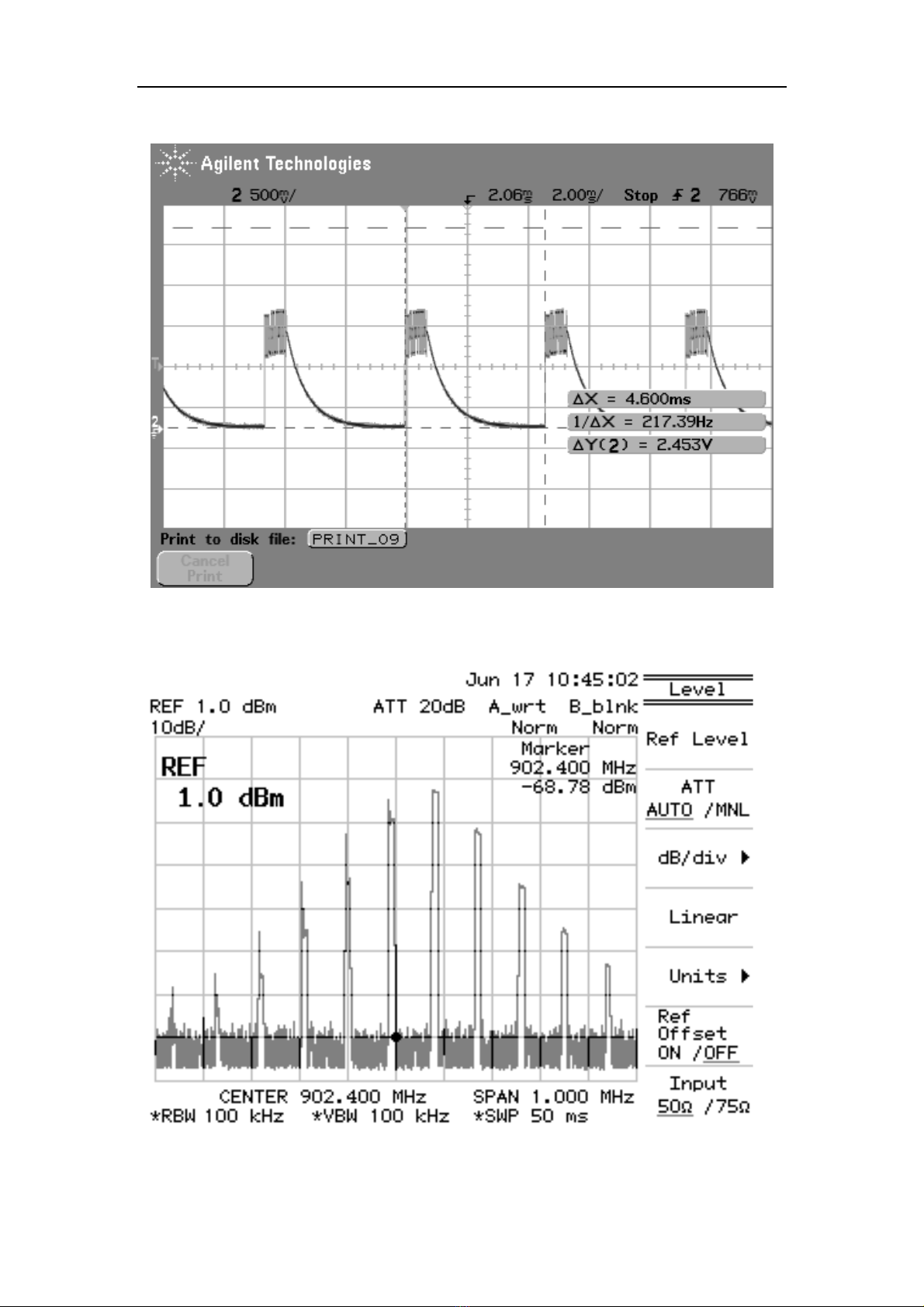
2.4COMMON RF MALFUNCTION....................................................................................................7
3BASEBAND..................................................................................................................................18
3.1BASEBAND OVERVIEW ...........................................................................................................18
3.2LOGIC.....................................................................................................................................18
3.3AUDIO FREQUENCY................................................................................................................18
3.4BLUETOOTH WIFI CIRCUIT.....................................................................................................21
3.5DUAL SIM –DUAL STANDBY SINGLE PHONE.........................................................................24
3.6ATV CIRCUIT..........................................................................................................................24
3.7BASEBAND COMMON MALFUNCTION ......................................................................................24
4REFERENCE FOR MAINTENANCE......................................................................................29
4.1NO SIGNAL .............................................................................................................................29
4.2PHONE DOES NOT “POWER ON”...............................................................................................29
4.3LCD TROUBLE........................................................................................................................29
4.4SOUND TROUBLE ....................................................................................................................29
4.5KEYBOARD MALFUNCTION.....................................................................................................29
4.6CAMERA WITH FLOWERY/BLANK SCREEN ...............................................................................29

E195ServiceMenu
1
1Overview E195
1.1 About E195 Phone
E195 mainboard is based on the MSTAR platform, which is supporting GSM/GPRS:
900/1800/850/1900MHz GPRS three-frequency communication. It is Dual SIM – Dual
Standby Single the mobile phone. The phone has the following feature:
1, Three specialties: 3.5 HVGA(resolution 320 * 480) LCM, 5M camera, ultrathin 10.9 MM
2, Dual SIM – Dual Standby Single PDA, compatible with three configurations: basic
configuration + WIFI + ATV
3, Support NOKIA specification device: BL- 5C battery, MICRO 5PIN interface
D201
MSW8533N
CPU
D104
RF7163 ASM
D1056
SI4210
TRANSCEIVER+PA
D301
H8ACS0PE0MBR-46
M-C
NAND+LPSDRAM
T-FLAHS-CART
LCM
摄像头
KEY
KEY_LED
RGB_LED
MOTR
B_LED
D608
ACRUX21
BT
D605
MSB7602
WIFI+BT
AUDIO
SENSOR

E195ServiceMenu
2

E195ServiceMenu
3
1.2 Distribution of the mainboard components

E195ServiceMenu
4

E195ServiceMenu
5
2RF
2.1 RF Overview
RF part mainly consists of transceiver AERO4210HN (adopts program of near-zero IF
receiver, supporting the EGSM / DCS and 26M VCTCXO as the clock input, integrated
clock buffer, LO VCO and TX VCO and regulator, only need for external connections of
VBAT / AVDD.
GSM RF and BB interface diagram
Transceiver (AERO4210HN) with the RF modulation and demodulation functions contains
IF frequency synthesizer and VCO RF, which is part of the core component of the RF. PA
has a major role in amplification of modulation signal, and it must be controllable and the
speed should meet the GSM agreement.
2.2 Transmit
TX is composed of the modulation loop, power amplifier and antenna switch. PLL is
mainly in the internal AERO4210HN, I / Q signal first enters into the AERO4210HN. After
entering the PLL the signal is modulated to RF, and then it outputs from the chip to PA,
converts into electromagnetic energy through antenna by the antenna switch after
enlarged.
PA:
This part adopts voltage control to achieve and its role is to amplify the signal power in
accordance with the requirements. It is divided to different power levels through VRAMP
signal. The transmit signal of GSM is 5 to 19, power is from 3.2MW to 2W while DCS is 0
~ 15, power from 1MW ~ 1W. PAis time-sharing work controlled by TX-EN chip, the output
power of PA is controlled by VRAMP (APC) through the voltage. PA is intermittent work, by
the BS to achieve the choice of frequency bands.
Baseband Chip

E195ServiceMenu
6
Host RF Launch Principle Diagram
2.3 Receive
Accessed from the antenna, GSM signal arrives at AERO4210HNN through the front end
SAW filter; and it converts to I/Q signal which modulated in 100 KHZ carrier. Then, it goes
through the band-pass, getting amplification (gain controllable), filtering, amplifier (gain
controlled); and mixes to baseband signal 4-road I/Q. Finally, it outputs to CPU for
processing after filtering. In diagram, SDATA, SCLK are I2C serial signals, responsible for
the communication work between MSW8533N and AERO4210HN; LE is MSW8533N
enable signal of AERO4210HN; RFVCOEN is enable signal which can generate
frequency mixing vibration signal VCO; VAFC is automatic frequency control signal of
crystal oscillator.
Host RF Receive Principle Diagram
I2C
I
Q
MT6129
MT6225
PA
同轴开关及
天线匹配电
ANT
匹配网
匹配网
GSM TX
路径
DCS TX
路径
频段选择信号
Transceiver
BB
AMS
RF 发射输出
RF Launch output
Coax
i
a
l
Sw
i
tc
h
&Antenna
matching circuit
Band selection signals
GSM TX Path
DCS TX Path
Transceiver

E195ServiceMenu
7
2.4 Common RF Malfunction
2.4.1 Detection and Maintenance Flow Chart of MS Transmit
malfunction
2.4.2 The maintenance process of Transmit malfunction
Use the Repair software and make mobile phone access to transmit state. Choose 62CH
in GSM band, POWER Level for 5, DCS for 700CH, POWER Level for 0. Then, first
observe whether the current rises, and use the spectrum analyzer and oscilloscope to
observe the signal given in the above-mentioned flow chart, the specific signal waveforms
shown as below:
Ch
ec
k
IQ
s
i
gna
l
i
nput
pin of Transceiver,
whether there is IQ
si
g
nal?
Check RF signal output
pin, whether there is
any RF signal?
Y
Check CPU
N
Y
Y
Check Transceiver,
whether there is any
RF out
p
ut si
g
nal?
N
VBAT, PA
_
EN,
BANDSW_DCS,
VAPC, are they OK?
Replace PA
Y
Check CPU
N
Replace
Transceiver
N
Check
Transceiver
External RC
Y
(No transmit) Connect PC and cell
p
hone with maintenance of line, use the
Repair software making mobile phone
access to transmit state.
Check antenna switch
or matching network

E195ServiceMenu
8
IQ signal waveforms of transceiver in transmit state:
3.10 I/Q
RF interface spectrum analyzer is as follows:
GSM transmit signal

E195ServiceMenu
9
DCS transmit signal
PA-EN waveforms of PA in transmit state:
PA-EN

E195ServiceMenu
10
PA. BAND-SW waveforms:
PA.BAND-SW (GSM)
PA.BAND-SW (DCS)

E195ServiceMenu
11
PA Vramp waveforms:
Vramp (pcl5)
Vramp (pcl 19)

E195ServiceMenu
12
2.4.3 Detection and Maintenance Flow Chart of MS Receive
malfunction
2.4.4 The maintenance process of Receive malfunction
Maintenance process of NO Receive: Use Repair software to make mobile phone access
to pure receive state →Choose 62CH, Rx Mode CH62=947.4MHZ, Input power:-60dbm
in GSM frequency bands →Choose 698CH, Rx Mode CH698=1842.4MHZ, Input
power:-60dbm in DCS frequency bands →Adjust signal generator to corresponding CH,
connect the signal line to Cable of RF →Measure the related key signal by using
Spectrum analyzer and Oscilloscope →Measure the signal output pin of Transceiver,
whether there is any correct IQ signal output to CPU →Y: Check CPU (MSW8533N) / N:
No Receive
Check CPU
Y
N
Are Transceiver
SDATA、SCLK、
LE、RFVCOEN all
correct?
Y
Check CPU
N
Whether the voltage
Transceiver used is
normal? Is 26MHz
normal?
Y
Check the
correspondi
ng power
supply and
circuits of
26MHZ.
N
Replace
Transceiver
Y
Whether PA signal
input pin has
received any
si
g
nal?
N
N
Check RX-filter
Y
Check Transceiver
External RC components
Check IQ signal output pin
of Transceiver, whether
there is IQ signal?
Check Transceiver input
pin, whether there is any
input signal?
Open Repair Software to connect PC with mobile phone, make the
phone access to receiving state, adjust signal generator to
corresponding CH, and connect the signal line to phone’s RX_SW.
Check or replace
antenna switch and
matching circuit

E195ServiceMenu
13
Check Transceiver input pin, whether there is any corresponding CH input signal (Y:
Check whether Transceiver has correctly controlled the signal →Check whether the
voltage supply is normal →if normal, Transceiver can be judged of damaged / N: Check
PA and the paths ahead ). Signal waveforms refer to the following:
Output signal of Signal generator (Input):
GSM CH62 channel receives the signal

E195ServiceMenu
14
DCS CH 698 channel receives the signal
IQ signal output pin of Transceiver the state of receiving IQ signal:
Test should have 2.8v voltage. The signal Transceiver received from CPU used to access
the internal register of Transceiver. The corresponding waveform is as follows:

E195ServiceMenu
15
3W(SDATA)
3W(SCLK)

E195ServiceMenu
16
3W(SCLK)
26M clock (can be measured by using the AC Coupling)
The RFCRTLCLK (automatic frequency control) from CPU to the crystal oscillator makes
26M crystal oscillator output accurate 26MHZ to Transceiver.
Crystal oscillator 26M input
26M outputs to CPU

E195ServiceMenu
17
VAFC
TCXO output(26MHZ)

E195ServiceMenu
18
3Baseband
3.1 Baseband Overview
E195 Baseband mainly consists of CPUMSW8533N. MSW8533N baseband, the core
device of the mainboard, is responsible for the normal work among various parts of
mainboard, such as voice processing, image processing and MS communications.
Digital baseband MSW8533N contains 2-bit ARM7E kernel, 284Kbyte SRAM.
MSW8533N is enhanced GSM processor, in the internal integration, including channel
codec, interleaving/solution intertwined, and the encryption/decryption, channel codec
subsystem; including ARM7EJS and peripheral interface circuit, control processor
subsystem. Its external has 26 roots address line, 16 data line, eight chip selection lines,
provide 6 external center fracture port; 26 M / 52 M operating clock.
Analog baseband contains MSW8533N analog baseband chip, audio and baseband
codec. Three major functional blocks integrated internal: Audio codec including Voice
input / Output channel, Buzzer output; Baseband codec including Differential I, Q input /
output, GMSK modulation and A / D, D / A; Auxiliary parts including AFC DAC, RAMP
DAC, AGC DAC and a seven-channel A / D. And WATCHDOG interface is set internal to
enhance the stability of the system.
3.2 Logic
Logic part is composed of MTK base-band management chip MSW8533N, Power
management chip and NOR Flash.
MSW8533N:CPU
NOR Flash:H8ACS0PE0MBR-46M-C
3.3 Audio Frequency
Because MSW8533N inside integrates the audio processing, which makes the
performance of sound quality more conspicuous pleasing.
3.3.1 Speaker loop
Relative to the AUDIO CODEC, Speaker loop is simpler, only a PA and SPEKER. When
maintaining, pay attention to the signal waveform of PA input and output end.

E195ServiceMenu
19
3.3.2 MIC loop
Check basic bias voltage signal of MICBIASP and MICBIASN and the language signal of
MIC itself when the MIC is good but no response of LOOP MIC in test.
Table of contents
Other FLY Cell Phone manuals