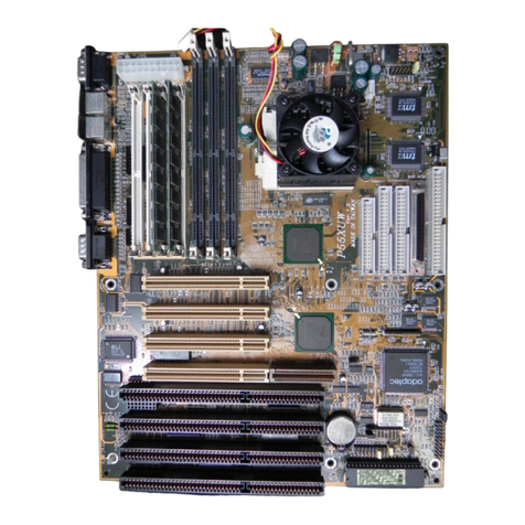
IWILL P55TV User manual

i
EC Declaration of Conformity
We
Iwill Corp.
No. 9-1, Kong 6th RD.,
Lin Kou 2nd Industrial
Park, Taipei, Taiwan R.O.C.
declare under sole responsibility that the
P55TV motherboard
meets the intent of Directive 89/336/ECC for Electromagnetic Compatibility.
Compliance was demonstrated to the following specifications as listed in the
official Journal of the European Communities:
EN 50081-1 Emissions:
EN 55022 Radiated, Class B
EN 55022 Conducted, Class B
EN 60555-2 Power Harmonics
EN 50082-1 Immunity:
IEC 801-2 Electrostatic Discharge
IEC 801-3 RF Radiat
IEC 801-4 Fast Transient

ii
About This Manual
This P55TV/TVS SCSI Motherboard is the newest member to our SCSI
Motherboard solution products families. It incorporated with Intel 4th generation
430VX Chipset and Adaptec
®
newUltra PCI SCSI AIC-7860(AHA-2940AU) that
double the SCSI speed. In order to support fully plug and play Ultra I/O , an Ultra
I/O that contain keybaord and real time clock is used for users to enjoy the plug
and play function.
Run with fasterCPU is very important function that thisSCSI Motherboard support.
It support both P54C up to 200 MHz* and Intel’s next generation P55C processor
that support MMX technology.
Run with faster system memory is another plus on this SCSI Motherboard to
outperform the whole system performance. It equipe 4 of the 72 pin SIMM that
support both fast page and EDO DRAM also with two of the 168 pin DIMM
memory socket that support the new synchonous DRAM.
This manual is subject to change without notice.
This manual contains information protected by copyright law. All right s are
reserved. No any part of this document may be used or reproduced in any forms
or by any means, or stored in a database or retrieval system, without prior written
permission.
Trademark
Intel
®
/ Pentium is trade mark of Intel
®
Corporation and allother product names
are trademarksand registered trademarksof their respective owners.
Warning
This motherboardis carefully designed with Intel
®
spec. to fully support P54C
processor up to 200Mhz and thenew P55C. Since Intel
®
is not shiping the P54C
with 200Mhz and the new P55C CPU at the point that we deliver this
motherboard so we hold the responsibility on if Intel changeany spec. that cause
the new processor not function properly in this motherboard.

iii
Contents
Chapter 1- Overview
1.1 Features P1
1.2 Specifications P3
Chapter 2- Quick Installation P4
Chapter 3- Hardware Installation
3.1 Preparation and Inspection P6
3.2 Placement P8
3.3 CPU group P11
3.4 Cache Memory P14
3.5 D-RAM Configuration P14
3.6 SCSI Interface P15
3.7 Creative Sound P17
3.8 IDE Interface P19
3.9 USB P19
3.10 Enhanced Multi-IO P20
3.11 Other P21
Chapter 4- Award BIOS Setup P24
4.1 Entering Setup P28
4.2 Standard CMOS Setup P31
4.3 BIOS Features Setup P35
4.4 Chipset Feature Setup P41
4.5 Power Management Setup P48
4.6 PNP/PCI Configuration P51
4.7 Integrated Peripherals P54
4.8 Load Setup Defaults P56
4.9 Supervisor/User Password P56
4.10 IDE HDD Auto Detection P57
4.11 HDD Low Level Format P57
4.12 Save & Exit Setup P57
4.13 ExitWithout Saving P57
Chapter 5- SCSI BIOS Setup
5.1 When to Use the SCSI Select Utility P58
5.2 SCSI Select Utility option P59
5.3 Configure / View Host AdapterSettings Menu P60
5.4 SCSI Disk Utilities P65


1
CHAPTER1
Overview
Thank you for purchasing this P55TV/TVS SCSI Motherboard. This operation
manual will guide you to proper configure and install. It has an overview of the
engineer design and feature of this board. Also, this manual provides useful
information for your later upgrade or change the configuration. Keep this, for
your future need.
1.1 Features
This P55TV/TVS SCSI Motherboard is a powerful combination of performance,
quality and innovative design to address the need of today’s market. With current
Intel P54C, Cyrix 6x86, AMD 5k86 and next generation on Intel P55C with
MMX technology supported, 512K external Level 2 Pipelined burst fast Write -
Back Cache, 64 bit Burst Bus DRAM and Adaptec Ultra SCSI (AHA-2940AU ),
fully plug and play Ultra I/O, this SCSI Motherboard brings exceptional
processing power that could only be achieved by Mini -computer. Incorporating
the new emerging industrial standard Peripheral Component interconnect (PCI)
Local Bus together with the standard 16-bit Industrial Standard Architecture
(ISA), this SCSI Motherboard dramatically boots system I/O through for even the
most demanding application in today’s market.
◼CPU:
CPU socket (socket 7) supports the flexibility of different typeof current
and future Intel Pentium, AMD (K5) and Cyrix (M1) processor. One easy
jumperdesign, while choosing your CPU speed from 75 to 200MHz.
◼Cachememories:
High performance write back secondary cache.This supports Pipelined
Burst Cache 512K on-board to achieve the highest performance.
◼BIOS:
Award BIOS, on-screen "Plug & Play" setup for Adaptec SCSI, Enhanced
IDE, and Ultra multi-IO. Support Flash ROM ( This ROM provides
better upgrade ability for user to update theirBIOS data on the system
board,user can down-load newer version BIOS from Internet or diskette
file.

2
◼Expansion slots:
5 X 16-bits ISA slots for P55TV, 4 X 16-bits ISA slots forP55TVS .
3 X 32-bits PCI slots for PCI compatible add-on cards.(PCI#2 is occupied
by the AdaptecSCSI, it is flexible for your choosewhile you install a prior
or minor controller on this PCI bus.) (PCI Rev 2.1)
◼Memories:
4 X 72-pin SIMM(Single In Line Memory Module)
2 X 168-pin DIMM(Dual In Line Memory Module) (Rev 1.1)
Support up to 128MB (minimum of 8MB ) on board.for both the Fast
Page Mode and Extended Data Output (EDO) module.
◼Ultra SCSI interface:
Built in Adaptec PCI Ultra SCSI ( AIC 7860chip ) which is the same
as Adaptec AHA-2940AU PCI SCSI controller.
Data transfer rate up to 20MB/Sec.
Complete software driver from Adaptec Inc., include EZ-SCSI for
DOS/Windows, Netware, Windows NT , OS/2 , SCO Unix ,
Unixware.
◼Creative Sound (P55TVS only):
Built in Creative Vibra CD quality stereo sound on board.(CT2505)
Wave table option.Reference to Chapter3.7 for more detail.
◼IDE functions:
Built in dualPCI Bus EIDE Channels.
Support ATAPI (AT Attachment Packet Interface)
◼USB interface (Universal Serial Bus):
Plug and Play outside the box
Up to 12Mbit
Easy of use
◼Floppy Interface:
Support both 3 1/2"and 5 1/4" floppy disk drives and Tape Drive
(360K / 720K/ 1.2M / 1.44M / 2.88MB)
Enabled/Disable selectable from system BIOS
Non-Burst ModeDMA Option,16 Byte Data FIFO
3 Mode Driver (option)
◼Serial Port
Two high speed 16550 UART serial port
IRQ selectable from BIOS.
Address changeableform system BIOS
NS16C550 compatible,Programmable Baud Rate Generator

3
◼Parallel Port
IRQ selectable for IRQ5(278h), IRQ7(378h) from system BIOS.
Standard mode--Compatible with IBM PC/AT Printer port
EPP Mode --Enhanced Parallel Port compatible(EPP) compatible
IEEE 1284
ECP Mode --Microsoft & Hewlett Packard Extended Capabilities Port
(ECP) Compatible
IncorporatesChiProtect Circuit for protection against damage due to
printer power-on
1.2 Specifications
◼Physical Dimensions:Length: 330mm / Width: 220mm
◼Environmental Requirements:
Temperature0-55 degrees C (operating or storage)
5% to 95% non-condensingrelative humidity
CHAPTER2

4
Quick Installation
This SCSIMotherboard isshippedwith
manufacturepresetat :
1. CPU Clock at 100 MHz
2. Adaptec Ultra SCSI Chip Enabled
3. SCSI Terminator Control by BIOS
4. 512K Pipeline Burst Cache on board
5. Printer ECP Mode at DMA3
6. Printer at IRQ7, Address at 378h
7. Serial 1 at IRQ4, Serial 2 at IRQ3
8. PS/2 MOUSE at IRQ 12
Referenceto the Chapter 3 & Chapter 4, if you
havedevices conflictwith themanufacturedefault.
Step 1. Install CPU and Cooler
Make sure the Clock Frequency is set to the same as theCPU
installed. (Choose the CPU speed by one jumperon JP15)
Step 2. Install the memory
Plug at least 2 PCS of 72 pins Micro Edge DRAM modules
or at least 1 piece of 168 pins DIMM.
Step 3. Install display controller and connect I/O ports
This system board is designed using PCI (Peripheral Component
Interconnect)and ISA (Industry Standard Architecture) interface
controller. This support +5Volt interface slots. All PCI interface
controllers must be PCI Rev 2.1 compliant.
Step 4. Connect the power supply
Connect P8 and P9 from power supply output.
Step 5. Power on the system
Turn on the Computerpower.
Step 6. Setting up the system

5
Enter the "Setup Menu" screen by press the " Del " key while
power on or warm reset the system.Always "LOAD SETUP
DEFAULT" at first and select others necessary that your
system require.
Step 7. Save the setup data to the CMOS
Exit the "Setup Menu " screen and then write to CMOS RAM.
And enjoy the high performance system board.
Step 8. After boot yoursystem O.S., insert the Adaptec EZ-SCSI
Installation diskette in a floppy disk drive and follow the EZ-
SCSI operation manualorreference to Adaptec 7800 Family
Set manualwhich will guide you to install the Netware,
Windows NT, OS/2 , SCO UNIX, Unixware.
CHAPTER3
Hardware Installation

6
3.1 Preparation and Inspection
The P55TV/TVS SCSI Motherboard,like all electronic equipment is static
sensitive. Please take theproper precautionswhen handling this board.You
should avoid static up. If possible, You should ground yourself by touching a
metaltableor yourcomputerframe.Keep the board in its conductivewrapping
until it is configured and ready to be installed in yoursystem.
For installation, you may need some or all of the following tools:
‧SCSI HDD drive/devices manual(s).
‧IDE HDD drive/devices and floppy drive manual(s).
‧Peripherals that connect to yoursystem's manual(s).
‧MS DOS diskettes with FDISK and FORMAT programs.
‧Medium size flat blade screwdriver.
‧Medium sized Phillips head screwdriver.
‧A 3/16 inch nut driver or wrench.
You should find the Following components when open thebox :
1. P55TV/TVS SCSI Motherboard.
2. This Operation Manual
3. Adaptec softwaredriver Diskette (EZ-SCSI).
4. Adaptec 7800 Family ManagerSet softwaredriver Diskettes.
5. Adaptec EZ-SCSI Manual.
6. Adaptec 7800 Family ManagerSet Manual.
7. Sound Input/Output adaptor(P55TVS only).
8. 50 pins internal SCSI signal flat cable.
9. Softwaredriver for CeartiveVibra sound.(P55TVS only).
10. 40 pins internal IDE signal cable.
11. 34 pins internal Floppy Disk Drive signal cable.
12. 10 pins IDC flat cableto 9 pins D-Sub male RS-232 connector.
13. 26 pins IDC flat cable to 25 pins D-Sub femaleprinter signal flat
cable.
14. 10 pins IDC flat cable to 25 pins D-Sub male RS-232 connector.
15. 1 x 5 pins IDC flat cableto L-frame 5 pins PS-2 mouseport.
16. Musical CPU Cooler.
17. External SCSI-2 port expansion kit (optional).
18. High speed printer port software driver(optional).
19. 3 Mode Driver (optional)
7
3.2 Placement

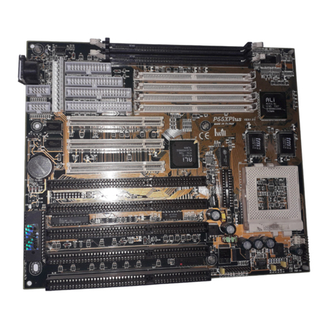
8
Placement & Connector
J3
1
J1
P55TV
PCI#4
Keyboard
PS2 mouse
PCI#3
PCI#1
1
Soocket 7
CPU
FAN
Speaker
Reset SW
SCSI LED
IDE LED
SMI SW
Turbo LED
Bank0
Bank1
Power CONN.
Ultra SCSI
Primary
IDE
Secondary
IDE
Floppy
COM#B
COM#A
Printer
USB
CONN.
Keylock

9
Placement & Connector
J3
1
J1
P55TVS
PCI#4
Keyboard
PS2 mouse
ISA
PCI#3
PCI#1
1
Soocket 7
CPU
FAN
Speaker
Reset SW
SCSI LED
IDE LED
SMI SW
Turbo LED
Bank0
Bank1
Power CONN.
Ultra SCSI
Primary
IDE
Secondary
IDE
Floppy
COM#B
COM#A
Printer
USB
CONN.
Sound AdaptorConnector
Keylock

10
Jumpers
1J1
P55TV/P55TVS
1
Soocket 7
7
59
0
1
0
0
1
2
0
1
3
3
1
5
0
1
6
6
1
8
0
2
0
0
JP7
1
1
JP3
JP5
1
P54C
P55C
JP10
1
JP17
1-2: Enable SCSI
2-3: Disable SCSI
1-2: Terminator alw ays On
Off: Terminator alw ays Off
2-3: Terminatorcontrol by BIOS
3.
5
2V
3.
3
8
2.
8
3
2.
7
0
2.
5
0
1-2: 12V Flash ROM(28xxx)
2-3: 5V Flash ROM(29xxx)
1
JP20

11
3.3 CPU group
3.3.1 CPU Socket
This CPU socket provides flexibility for Intel Pentium , Pentium
OverDrive, Pentium futureprocessors, AMD K5(5k86) and Cyrix
M1(6x86)processor. When installing the CPU into the Zero Insertion
Force ( ZIF ) socket should be very carefully. Lift the handleof this 321
Pin ZIF socket up carefully and insert theCPU into ZIF socket. And make
sure the CPU Pin 1 is with the squarebase and it goes to particularhole on
the ZIF socket. Once you match the hole with Pin 1 then gently insert the
CPU and press socket handle down.
Pentium
pin #1
Socket 7
3.3.2 J17 CPU Cooler Fan PowerConnector
Warning !!! Warning !!! Warning !!!
CPU Cooler is required to be placed on top of
the CPU all the times to prevent CPU over-heat.

12
The CPU fan power connector is a 1 x 3 pin.
Pentium
pin #1
Soocket 7
J17
J17 Pin
+12V
GND
Control
3.3.3 CPU Clock Select

13
JP15 is a 2 X 9 pin jumper, with one"colored" jumpercap on it. One and
only one jumpercap need to put on this connectorforselecting the CPU
clock. Just put the colored yellow jumpercap to the speed yourCPU really
is (the CPU internal/externalclock ratio and ISA clock will be
automatically selected by setup the JP15)
JP15
7
5
9
0
1
0
0
1
2
0
1
3
3
1
5
0
1
6
6
1
8
0
2
0
0
MHz
Regarding Cyrix CPU clock setting, please referto Appendix A for detail.
3.3.4 CPU Voltage Select (JP10)
The default 3.38V is for most CPU that runs3.3V. Others voltage is
reserved forfuture and otherbrand CPU use. Check your CPU vendorfor
more information.
Pentium
Socket 7
3.38 (default)
3.52V
2.83
2.70
2.50
JP10
JP5
P54C
1
JP20
1
(default)
or
Pentium
Socket 7
3.38
3.52V
2.83
2.70
2.50
JP10
JP5
P55C
1
JP20
1
3.3.5 P54C/P55C Select (JP5 & JP20)
CPU
JP5
JP20
Note
P54C/P54CS/P54CT
2-3, 2-3
2-3
*Default
P55C
1-2, 1-2
1-2
3.4 Cache Memory

14
The cache memory support for pipilined burst SRAM, this will peerform at
least 10% fasterthan traditionalasynchronousSRAM. Manufacture default is
512K on-board.
3-5 D-RAM Configuration
M1
M2
M3
M4
BANK 0 Socket 1
BANK 0 Socket 2
BANK 1 Socket 3
BANK 1 Socket 4
BANK 0 Socket 5
BANK 1 Socket 6
D
I
M
M
1
D
I
M
M
2
The P55TV/TVS supports different type of system memory.No jumperneeded for
this function or configure. This mainboard separates four pieces of 72 pins
SIMM(Single In Line Memory Module) into two banks, and also two pieces 168
pins DIMM(Dual In Line Memory Module) into two banks, they use the same
address. This means the Bank 0 and Bank 1 only can recognize either two pieces
of 72 pins SIMM or one pieces of 168 pins DIMM on each bank.
NOTE:
1
. P55TV/TVS support both Fast Page DRAM or EDO
DRAM SIMM/DIMMs also the ECC are supported,but they
cannot be mixed within the same memory bank.
2
. They arethe samein Bank 0 or Bank 1. Socket 1,2 and
socket 5 are using the same memory block (Bank 0). They
can not install in the same time. Socket 3,4 and socket 6 are
using the same memory block (Bank 1).
3
. The 70 ns Fast Page Modeor 60 ns EDO DRAM is
recommended.
4
. DIMM specification: 3.3V/ Unbuffered
5. This motherboard supports4 Clock for each DIMM Socket

15
Left Key Zone
(Unbuffered)
Center Key Zone
(3.3V DRAM)
Make sure the DIMM module is 3.3V/ Unbuffered and support the Intel Pentium
processor while you insert into the DIMM socket.
Note: End user should not populate both 5V SIMM modules & 3.3V DIMM
modules at the same time.
3.6 SCSI Interface
3.6.1 J2 Ultra SCSI Connector
J2 is a 50 pins 16 bit internal Ultra SCSI connector. ItattachestheSCSI
cable(s) from theP55TV/TVS SCSI controller to the SCSI peripherals.
The externalSCSI port expansion kit is a optionalfor your connecting
externaldevices. Be-sure thecable's colored side should align to pin #1 of
this connector.
1
2
49
50
3.6.2 Link Internal & External SCSI devices
The SCSI devices are cabled together in a single, connected series. This
SCSI cable must run sequentially from one device to the next,with no
branches.

16
P55TV/TVS
Internal SCSIdevices
External SCSIdevices
Host=ID7
50pin flat SCSIcable
External SCSIexpansion kit
*Reference to Chapter5. SCSI Select Utility for softwaresetup.
3.6.3 Set SCSI IDs
You must assign a different SCSI ID to each device on the SCSI bus
connected to the P55TV/TVS system board.See yourSCSI device
documentation fordirections on how to determine the ID and changeit.
◼ Ultra/ Fast SCSI devices that connect to this mainboard'sSCSI
connectorcan be assigned ID from 0 to 7. Normally, the host will use ID7.
Or reference to Chapter5 for moreinformation.
◼ The SCSI ID0 is best use for SCSI harddisk to beused as your
computer'sbootdevice, ID1 is best reserved for a secondary SCSI hard
disk.(This is only when you use the SCSI hard disks and devices.)
3.6.4 SCSI Chip Select
JP7 is a 3 pin jumper connector.
Function
JP7
Note
Enabled
1-2
*Default
Disabled
2-3
3.6.5 SCSI Terminator Control
JP3 is a 3 pin jumper connector.This is for SCSI Terminator.
Function
JP3
Note
Terminatoralways On
1-2
Terminatoralways Off
off
TerminatorControlled by BIOS
2-3
*Default
3.6.6 SCSI LED
Other manuals for P55TV
1
This manual suits for next models
1
Table of contents
Other IWILL Motherboard manuals

IWILL
IWILL kv200 User manual

IWILL
IWILL DP533 Series User manual

IWILL
IWILL DS133R User manual

IWILL
IWILL KK266Plus User manual

IWILL
IWILL WO2 Original operating instructions

IWILL
IWILL VD133 Pro Series User manual

IWILL
IWILL DK8S User manual

IWILL
IWILL DX400-SN User manual

IWILL
IWILL UPX User manual

IWILL
IWILL DPIILS2 User manual

IWILL
IWILL P55TU User manual

IWILL
IWILL DN800-SATA User manual

IWILL
IWILL DGL200 User manual

IWILL
IWILL FB24624100 User manual

IWILL
IWILL VD133 User manual

IWILL
IWILL Motherboard DJ800 User manual

IWILL
IWILL BD100 Plus User manual

IWILL
IWILL DVD266 User manual

IWILL
IWILL DK8X User manual

IWILL
IWILL KK266 User manual