IWILL P55XB2 User manual

1
EC Declaration of Conformity
We
Iwill Corp.
No. 9-1, Kong 6th RD.,
Lin Kou 2nd Industrial
Park, Taipei, Taiwan R.O.C.
declare under sole responsibility that the
P55XB2 motherboard
meets the intent of Directive 89/336/ECC for Electromagnetic Compatibility.
Compliance was demonstrated to the following specifications as listed in the
official Journal of the European Communities:
EN 50081-1 Emissions:
EN 55022 Radiated, Class B
EN 55022 Conducted, Class B
EN 60555-2 Power Harmonics
EN 50082-1 Immunity:
IEC 801-2 Electrostatic Discharge
IEC 801-3 RF Radiat
IEC 801-4 Fast Transient

2

3
About This Manual
This manual will guide the user on how this new Ultra ATA ( Ultra DMA 33 )
motherboard was manufactured. All useful informations will be described in later
chapters. Keep this manual for your future upgrade or system configuration changed.
The chapter Quick Installation ---
This chapter’s description is suitable for most user, Just follow step by step in
installing the system.
The chapter Overview ---
Describe the feature and specificaton of this Ultra DMA 33 motherboard.
The chapter Hardware Installation ---
Describes the hardware detail specification and connection.
The chapter Award BIOS Setup ---
Detail description of this Ultra DMA 33 motherboard, no need to change the
manufacture default unless you have conflict in your system.
The chapter Appendix ---
Useful information will be added in this chapter for your reference.
Warning
This motherboard is carefully designed with Intel spec. to fully support Pentium processor with MMX up
to 233Mhz . Since Intel is not shiping the new Pentium procesoor with MMX with 233Mhz at the time that
we deliver this motherboard so we hold the responsibility on if Intel change any spec. that cause the new
processor not function properly in this motherboard.

4
Trademarks
IWILL, the IWILL logo, RAIDBUS are trademarks of IWILL Corporation which is registered in the
United State of America and some other countrys with some jurisdictions.
Intel, the Intel logo, Pentium are trademarks of Intel Corporation.
Adaptec, the Adaptec logo are trademarks of Adaptec, Inc.
Microsoft and Windows are trademarks of Microsoft Corporation
All other trademarks are owned by their respective owners
Copyright
Copyright 1997 IWILL Corporation. All right reserved. No part of this publication may be reproduced,
store in a retrieval tape, disk, system or transmitted in any form or by any means, electronic, mechanical,
photocopying, recording or otherwise, without the prior written consent of IWILL USA Corporation. 1542
#B Edinger , Tustin, CA 92680
Changes
The content in this manual document is for the information only and is subject to change without notice.
IWILL Corporation assumes no liability resulting from errors or omissions in this document or from the
use of the information contained herein, even reasonal efforts had been made in the preparation of this
manual.
IWILL Corporation reserves the right to change the product design without reservation and without
notification to its users.

5
Contents
Chapter 0- Quick Installation P5
Chapter 1- O er iew P16
1.1 Features P16
1.2 Specifications P19
Chapter 2- Hardware Installation P20
2.1 Preparation and Inspection P20
2.2 Placement P21
2.3 CPU group P23
2.4 Cache Memory P28
2.5 D-RAM Configuration P28
2.6 IDE Interface P30
2.7 USB P31
2.8 Enhanced Multi-IO P32
2.9 Other P34
Chapter 3- Award BIOS Setup P38
3.1 Entering Setup P41
3.2 Standard CMOS Setup P44
3.3 BIOS Features Setup P48
3.4 Chipset Feature Setup P53
3.5 Power Management Setup P60
3.6 PNP/PCI Configuration P64
3.7 Integrated Peripherals P67
3.8 Load Setup Defaults P69
3.9 Supervisor/User Password P70
3.10 IDE HDD Auto Detection P71
3.11 HDD Low Level Format P71
3.12 Save & Exit Setup P71
3.13 Exit Without Saving P71

6
CHAPTER 0
Quick Installation
Several easy installation steps will be described in this chapter to help the experienced
users for quick installation. If you are new user and need to know more about this
motherboard, please start from Chapter 1.

7
ISA
PCI
FDD
S. IDE
P. IDE
J8
J2
LPT
ATX
AT
S. 2
KB PS2
CPU
BIOS
P. Control
Fan
USB
IR
J4
J7
J9
J11
S. 1
Figure 1:Connectors for P55XB2

8
75*
90
100
120
133
150
166
180
200
233
266
JP7
JP4
JP3
JP16
JP15
Figure 2 : Jumpers location

9
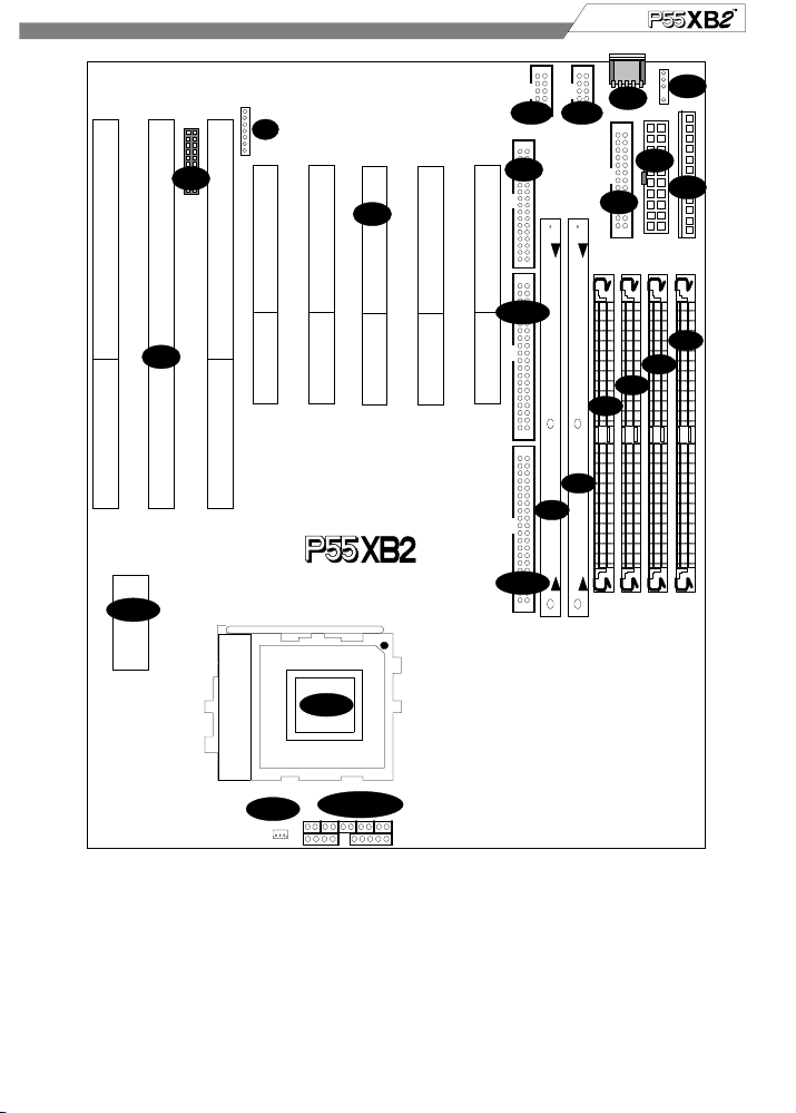
Connector Function Description
ATX 20 pin Standard ATX power input connector
AT 12 pin Standard AT power input connector
B1 Bank 1, each bank consist by two SIMM Socket(Single In-line
Memory Module )
B2 Bank 2, each bank consist by two SIMM Socket(Single In-line
Memory Module )
BIOS BIOS (Basic Input Output System)
CPU 321 pin Socket 7 CPU socket
D. 1 DIMM1 (Dual In-line Memory Module ) Bank 0
D. 2 DIMM2 (Dual In-line Memory Module ) Bank 1
Fan 3 pin CPU Cooler fan connector
FDD 34 pin Floppy Disk Drive with key protect connector
LPT a 2 x 13 pin box header for Parallel port connector
ISA 3 x ISA(Industrial Standard Architecture) 98 pin expansion slot
IR a 7 pin pin-header for Infrared port connector
KB 5 pin keyboard DIN connector
P. IDE40 pin box-header for Primary IDE connector
PCI 5 x PCI version 2.1 compliance 120 pin PCI (Peripheral
Component Interface)expansion slot
P. Control Front panel signal control connector
RST—Reset Switch
IDE—IDE detect LED
SMI—System Management Interface switch
LED—Power-on LED
Speaker—Speaker connector
Keylock— Keylock switch connector
PS2 4 pin pin-header for PS2 connector
S. IDE 40 pin box-header for secondary IDE connector
S1 a 2 x 5 pin box-header for Serial 1 port connector
S2 a 2 x 5 pin box-header for Serial 2 port connector
USB 20 pin Universal Serial Bus connector

10
Jumper Setting
JP4 CPU Voltage Select
JP7 CPU Frequency select
JP3 CPU Voltage Monitor Jumper
JP16 CMOS Clear Jumper
JP15 Remote power switch for ATX Power
Manufacture Default Setting
CPU Clock CPU Clock at 166Mhz
CPU Voltage CPU Voltage at Auto Setting
Cache Size 512K Pipelined Burst Cache on board
Printer Port DMA3 for ECP Mode, Address=378h at IRQ7
Serial Port Serial l Address=3F8h at IRQ4,
Serial 2 Address=2F8h at IRQ3
PS/2 Mouse PS/2 Mouse at IRQ12
USB Disabled by BIOS, at PCI INTD (shared IRQ with PCI#4)

11
Quick Installation
Step 1. Install CPU
Pull up the CPU handle bar, place the CPU into the socket in gentle/ horizontal
way then pull down the handle bar back to its original place. Care must be
taken for the CPU’s direction when was inserted.
PCI
JP6
Step 2. Install CPU Cooler
Hook the CPU Cooler’s metal latch one side to the CPU socket’s peg, then
press the metal latch again to fit into another side.
Warning: Care must be taken when the CPU Cooler was installed, if not a
suitable force might scrach this motherboard.
Step 3. Adjust the CPU Voltage
The manufacture default in jumper 4 is “Auto”, this motherboard will detect
voltage automatically.
In order to support more and more future Pentium compatible processor
Voltage, this motherboard design also reserved user selectable voltage instead
of “Auto” function. In case of the new CPU can not be detected on the voltage
by this motherboard’s BIOS, user need to set the CPU Voltage manually.
Intel Single Voltage ( P54C ) CPU set to 3.38V on STD and 3.52V on VRE.
AMD,Cyrix Single Voltage CPU all set to 3.52V

12
All Intel Dual Voltage ( P55C, 166 / 200 / 233Mhz ) CPU set to 2.83V.
AMD Dual Voltage ( K6, 166 / 200Mhz ) CPU set to 2.9V
AMD Dual Voltage ( K6, 233Mhz ) CPU set to 3.2V
Cyrix Dual Voltage ( M2, 166 / 200 Mhz ) CPU set to 2.83V
JP4
JP4
Auto
2.83
2.90
3.00
3.10
3.38
3.52 V

13
Step 4. Adjust the CPU Frequency
The manufacture default at 166Mhz with the special design on this
motherboard. Once the jumper cap was inserted, it will automatically caculate
the Internal/ External Clock and CLKMUL (Clock Multiplier). Just insert the
jumper cap to the CPU real frequency. There are more detail description on
Chapter 3.3.3 CPU Clock Select and Appendix A CPU for more information.
75*
90
100
120
133
150
166
180
200
233
266
JP7
JP7
90
100
120
133
150
166
Cyrix
200
233
266
110
Step 5. Install the Memory Module
For at least two pieces 72 pin SIMM(Single In-line Memory Module) or one
piece 168 pin DIMM(Dual In-line Memory Module ) must inserted in this 64
bit Pentium base motherboard.
The memory in this motherboard devided into three banks. The right side two
pieces of SIMM socket combined as bank 0, the left two pieces of SIMM
socket is the same address with the right side of DIMM socket they both
occupy bank 1 (memory will not added together if both these socket were all
inserted). The left DIMM socket is occupied by bank 2.
The two pieces of the SIMM in the left side are occupy the Bank 0, it is the
same address with the DIMM 1. The left side two pieces of the SIMM are
occupy Bank 1. The system memory will not added together, if the memory
were put into the same bank.

14
PCI
Bank 1
Bank 0
DIMM 0= Bank 0
DIMM 1= Bank 1
J2
J4
J7
J9
J8
J11
Step 6. Install the Internal Peripherals
The internal peripherals means devices that in the computer chassis like the
Floppy Disk Drive, Hard Disk Drive, CD ROM Drive …etc. With this
motherboard package, there are 34, 40, pin flat cable. Use these cables to
connect the motherboard and internal devices. All flat cable’s connector
housing have the key protect, this will guide you the correct direction when
you insert.
PCI
Step 7. Install the External Peripherals
The external device means devices that outside the computer chassis like the
Serial mouse, Printer, PS/2 Mouse, External Modem…etc. With this
motherboard’s package there are two 10 pin cables convert to 9 and 25 pin D-

15
Sub male connector cable are for Serial port, one 26 pin convert to 25 pin D-
Sub female connector cable is for Parallel port, one 5 pin housing but 4 wires
into a 6 pin Mini-DIN is for the PS/2 mouse.
Step 8. Connect the SMI
(System Management Interrupt)
Switch
Some computer chassis provides a SMI switch from front pannel, connect this
2 pin wire to this SMI switch(any direction can function this). This will force
the system into a Suspend mode/ Green, to decrease electricity and longer life
of component that not in use. Or the user can use chassis that still provides the
Turbo switch and functionless on current motherboard.
Once the SMI switch was pushed, this will force the system into the “suspend
mode” immediately. Any key strike on the keyboard will wake system up.
PCI
RST
IDE
SMI
LED
SPEAKER KEYLOCK
1
1
1
Step 9. Connect the Reset switch
Most computer chassis provides a reset switch to front pannel control, this will
reboot the system without turn off and on the power switch while the reset
switch was pushed. Use the chassis provides a 2 pin housing and connect to
this reset switch (any direction can function this).
Step 10. Connect the Keylock
(keyboard lock)
Switch
Most computer chassis will provides a keylock switch. Normally, connect the
marked keylock connector to this motherboard’s keylock connector. This will
cause the keyboard out of function once you switch the keylock to “Lock”.
This will prevent any un-authorized keyin. The onboard keylock connector
was a 5 pin pin-header, connect to the right side two pin will function this.
(Reference to the Chapter 3—Hardware Installation for detail pin assignment)

16
Step 11. Connect the Speaker
Connect the speaker to the motherboard’s speaker connector. (Normally the
red cable is +5V power) (Reference to the Chapter 3—Hardware Installation
for detail pin assignment)
Step 12. Connect the Power LED
Most computer chassis provides a power LED for identify if the system is on
or off. Connect the power LED to the 2 pin pin-header motherboard’s LED
connector. (normally the red cable is +5V power)
Or connect to the left side of
onboard keylock .(Reference to the Chapter 3—Hardware Installation for
detail pin assignment)
Step 13. Connect the Devices LED
Some computer chassis provides device LED(Like HDD LED) for identify if
the device is under working or not. Connect the device LED to the
motherboard’s IDE device LED connector. (normally the red cable is +5V
power)
Step 14. Connect the Power Input
This motherboard provides two types of power input; the AT & ATX for
different choises.
The AT switching power provides 2 sets cable P8 & P9 (6 pin for each set)
and ATX power provides 1 set 20 pin cable for motherboard’s power input.
Step 15. Connect the ATX Power Switch
This motherboard provides a 2 pin connector for connecting a momentary
switch for the system on/off.
JP15
JP15

17
Step 16. Connect the Keyboard
Follow the keyboard cable’s key direction and connect to this motherboard.

18
Step 17. Plug the Display Card
Finally, follow the display card you have and insert in horizontal direction
into the PCI/ISA expansion slot.
Step 18. Power on the system
Once the system was power on, on the lower left corner of the screen will
show ”Press DEL to enter SETUP, ESC to skip memory test”. Then press
“DEL” to enter BIOS setup for the first time power on and choose the “LOAD
SETUP DEFAULTS” then BIOS will responds “Load SETUP
default(Y/N)?”, press “Y” and “Enter”. Final choose “SAVE to CMOS and
EXIT (Y/N)?” by pressing “Y” and “Enter”.

19
CHAPTER 1
Overview
Thank you for purchasing this P55XB2 Ultra DMA33 Motherboard. This operation
manual will guide you to proper configure and install. It has an overview of the
engineering design and feature of this board. Also, this manual provides useful
information for your later upgrade or change the configuration. Keep this, for your
future reference.
1.1 Featuress
This P55XB2 Ultra DMA 33 motherboard is your best choice for optimized media
rich performance desktop on the Pentium® level processor with the new MMX™
technology. It incorported with Intel’s 430TX PCIset with I/O subsystem that
supports for pentium processor from 75 to 233 MHz with one single jumper to set up
the frequency and 512Kbyte for 2
nd
. Level Cache onboard that well prepare to run
heavy application.
The concurrent PCI (PCI 2.1) reduces CPU latencies for smoother video and more
relistic audio and Universal Serial Bus (USB) technology makes Plug and Play
peripheral connections a reality.
Run with faster system memory is another plus on this Pentium EIDE Motherboard to
outperform the whole system performance. It equipe 4 of the 72 pin SIMM that
support both fast page and EDO DRAM also with two of the 168 pin DIMM
memory socket that support the new 3.3V, unbuffered Synchonous DRAM.
The onboard two enhance IDE channels support for UltraDMA/33 that support data
transfer to 33 MBytes which this new technology but is compatible with the existing
ATA-2 IDE specification.
Fully support plug and play I/O that contain two high speed serial ports, one
ECP/EPP printer port, up to 2.88 floppy disk port, keyboard and real time clock is
used for users to enjoy the plug and play function. This Pentium EIDE motherboard
has designed with AT form factor to improve the easy access memory module, long

20
add-on card support and some of the new features that traditional AT form factor can
not achieved.
This P55XB2 Ultra DMA 33 Motherboard is designed to fit into standard AT form
factor based computer case. It is a powerful combination of performance, quality and
innovative design to address the need of today’s market. With current Intel P54C,
Cyrix 6x86, 6x86L, AMD 5k86 and next generation on Intel P55C with MMX
technology supported, 512K external Level 2 Pipelined Burst Fast Write-Back Cache,
64 bit Burst Bus DRAM and enhanced IDE with 2 channels and plug and play Ultra
I/O, this EIDE Motherboard brings exceptional processing power that could only be
achieved by Mini-computer. Incorporating the new emerging industrial standard
Peripheral Component interconnect (PCI) Local Bus together with the standard 16-bit
Industrial Standard Architecture (ISA), this SCSI Motherboard dramatically boots
system I/O through for even the most demanding application in today’s market.
CPU:
CPU socket (socket 7) supports the flexibility of different type of current
Cyrix (M1, M2), AMD (K5, K6) and Intel
Pentium, Pentium with MMX
processor. One easy jumper design to set the CPU frequency while choosing
your CPU speed from 75 to 266MHz.
BIOS:
Award BIOS, on-screen "Plug & Play" setup for Enhanced IDE, and Ultra
Multi-IO. Support Flash ROM ( This ROM provides better upgrade ability
for user to update their BIOS data on the system board, user can down-load/
update newer version BIOS from Internet or diskette file.
Cache memories:
High performance write-back 2
nd
. Level external static RAM cache. This
supports 512KB Synchronous Pipelined Burst Cache on-baord.
Memories:
4 X 72-pin SIMM (Single In Line Memory Module)
2 X 168-pin DIMM (Dual In Line Memory Module) (Rev 1.1)
Support system memory up to 256MB (minimum of 8MB ) on board with
either fast page mode, EDO under SIMM socket or the new Synchronous
DRAM with DIMM socket (3.3V un-buffered type).
Expansion slots:
This motherboard provides :
Table of contents
Other IWILL Motherboard manuals

IWILL
IWILL DPIILS2 User manual

IWILL
IWILL P4E Series User manual

IWILL
IWILL mp4s Original operating instructions

IWILL
IWILL K7S3 Series User manual

IWILL
IWILL P4G Series User manual

IWILL
IWILL IWILL P4D-N User manual

IWILL
IWILL KD266 User manual

IWILL
IWILL DPL533 User manual

IWILL
IWILL DVD266 User manual

IWILL
IWILL P4R533 User manual

IWILL
IWILL VD133 Pro Series User manual

IWILL
IWILL DK8N User manual

IWILL
IWILL mP4G2 Series User manual

IWILL
IWILL DH800 User manual

IWILL
IWILL P4SE2 User manual

IWILL
IWILL dca200 User manual

IWILL
IWILL P55XPLUS User manual

IWILL
IWILL wa133 User manual

IWILL
IWILL PIINS User manual

IWILL
IWILL WO2 Original operating instructions