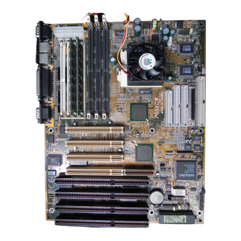
IWILL P6NS User manual

i
EC Declaration of Conformity
We
Iwill Corp.
No. 9-1, Kong6th RD.,
Lin Kou 2nd Industrial
Park, Taipei, Taiwan R.O.C.
declare under sole responsibility that the
P6NS motherboard
meets the intent of Directive 89/336/ECC for Electromagnetic
Compatibility. Compliance was demonstrated to the following
specifications as listed in the official Journal of the European
Communities:
EN 50081-1 Emissions:
EN 55022 Radiated, Class B
EN 55022 Conducted, Class B
EN 60555-2 Power Harmonics
EN 50082-1 Immunity:
IEC 801-2 Electrostatic Discharge
IEC 801-3 RF Radiat
IEC 801-4 Fast Transient

ii
About This Manual
This P6NS PPro SCSI Motherboard is the newest memberto our SCSI
Motherboard solution products families. It incorporated with new Intel generation
82440FX Chipset and with Adaptecnew Ultra / Ultra Wide SCSI embedded
which is equilevent to AHA 2940UW. AdaptecRAID port option ready is a big
advantagein this P6NS PPro SCSI motherboard.It can turn this SCSI
motherboard to supporthardwareSCSI RAID by addingthe RAIDBUS 1000 or
the ARO 1130 adapterfrom Adaptec.
This SCSI motherboard incorporated with Intel new 440FX Chipset which is PCI
Rev. 2.1 Compliant and supportwide range of the DRAMs include Fast Page,
EDO , Burst EDO DRAM type with SIMM socket. With 6 SIMM sockets
available,it is very flexible for customerto configure the system memory from
8MB up to 512MB.
Run with the new Intel Pentium Pro based CPU is the most important feature that
this motherboard provide.It support Intel Pentium Pro from 133Mhzup to
233Mhz.
Featurewith Error Check Correction ( ECC ) system memory is anotherplus on
this P6NS PPro SCSI Motherboard to outperform the whole system stability. It
equip 4 of the 72 Pin SIMM that support Fast Page, EDO or BEDO DRAM with
ECC.
This manualis subject to changewithout notice.
Trademark
Intel
®
/ Pentium is trade mark of Intel
®
Corporation and all otherproduct
namesaretrademarksand registered trademarksof their respective owners.

iii
Contents
Chapter 1 - Overview
1.1 Features........................................................... P1
Chapter 2 - Quick Installation ........................................ P5
Chapter 3 - Hardware Installation
3.1 Prepare & Inspection ....................................... P7
3.2 Placement ........................................................ P8
3.3 Block Diagram ................................................. P12
3.4 CPU group ...................................................... P13
3.5 Integrated PCI Bridge ...................................... P15
3.6 SCSI Interface ................................................. P16
3.7 Adaptec RAIDport option ................................. P19
3.8 IDE Interface ................................................... P20
3.9 USB ............................................................... P21
3.10 Enhanced Multi-I/O .......................................... P21
3.11 Other .............................................................. P23
Chapter 4 - ATX Form-Factor Overview ..................... P26
Chapter 5 - Award BIOS SETUP
5.1 Main Menu ...................................................... P34
5.3 Standard CMOS Setup .................................... P37
5.3 BIOS Features Setup ...................................... P41
5.4 Chipset Features Setup ................................... P47
5.5 Power Management Setup ............................... P55
5.6 PNP/PCI Configuration .................................... P55
5.7 Integrated Peripherals ..................................... P62
5.8 Load Setup Defaults ......................................... P64
5.9 Change Supervisor or User password................ P64
5.10 IDE HDD Auto Detection ................................. P65
5.11 HDD Low Level Format ................................... P65
5.12 Save & Exit Setup ........................................... P65
5.13 Exit without saving .......................................... P65


1
CHAPTER1
Overview
Thank you for purchasing this P6NS PPro SCSI Motherboard. This operation
manualwill guide you to proper configure and install. It has an overview of the
engineer design and feature of this board.Also, this manualprovidesuseful
information foryour later upgradeor changethe configuration.Keep this, for
your futureneed.
1.1 Features
This P6NS PPro SCSI Motherboard is a high performance on IntelPentium
Pro system hardware based motherboard.Both quality and innovative design to
address the need of today’s market. With various out-put voltage for Pentium Pro
level CPU supported,64 bit Burst Bus DRAM, Built-in AdaptecWide/ Ultra
Wide SCSI(AHA-2940UW) and Plug & Play Super I/O, this motherboard brings
exceptionalprocessing power that could only be achieved by Mini-computer.
Incorporatingthe new emerging industrial standard PeripheralComponent
Interconnect (PCI) Local Bus together with the standard 16-bit Industrial
Standard Architecture (ISA), this motherboard dramatically boots system I/O
through for even the most demanding a pplication in today’s market. The
hardwaredimension is Full ATX form factorwith fourlayer design technology.
The IntelPentiumPro Processor is the 6th generation in the Intel386, Intel
486, and Pentium family of processors. The Pentium Pro Processor hasseveral
key featuressuch as 12-stage super pipeline architecture, Built-in 256KB/512KB
cache,Out of order execution, dynamicbranch prediction & speculative
execution and a pipestage time 33 percent less than the Pentium Processor, which
helps achieve a higher clock rate on any given Process. It will be super pipeline
for high clock speed from 150MHzup to 233MHz.The Pentium Pro Processor
was used to theDynamicExecution that is the combination of improved branch
prediction, speculativeexecution and data flowanalysis that enablesthe Pentium
Pro processor to deliver its superior performancefrom CPU architecture.
The Pentium Pro Processor is a 64 bit processor with RISC technology. It
requires 32-bit applications(like Microsoft Windows NT and OS/2) to optimize
its capabilities and performances.The Pentium Pro processor delivers best value
2
for businesses moving to 32-bit computingwhen using the 32-bit Operating
System and Applications.
◼CPU
Intel Pentium Pro Processor operating at 150 ~ 233 MHz with 387 ZIF
socket 8 is scalableto accept fasterProcessors in the future. The Pentium
Pro Processor is the next in the Intel386,Intel486,and Pentium family of
processor. The second Level Cache(L2), controller are some of the
componentsthat existed in the Pentium Pro Processor.
◼Memories
Supports up to 512 Mega Bytes DRAM(minimum of 8 MB) onboard(72
Pin SIMM x 4, and BIOS auto FP DRAM, EDO and Burst EDO DRAM
detection and configuration.
◼BIOS:
Award BIOS, on-screen "Plug & Play" setup forAdaptec SCSI, Enhanced
IDE, and Super multi-IO. Support Flash ROM ( This ROM provides
better upgrade ability for user to updatetheirBIOS data on the system
board,user can down-load newer version BIOS from Internet,BBS or get
the diskette file from your vender.
◼Expansion slots:
1 X 16-bits ISA slots.
X 32-bits PCI slots for PCI compatible add-on cards.(PCI#2 is
occupied by the Adaptec SCSI, it is flexible for your choose while you
install a prior or minor controller on this PCI bus.)
1 X RAID port bus slot
◼Ultra/ Ultra Wide SCSI interface:
Built in Adaptec PCI Ultra Wide SCSI ( AIC 7880chip ) which is
equilevent to Adaptec AHA-2940UW PCI SCSI controller.
Data transfer rate up to 40MB/Sec.
Complete software driver from Adaptec Inc., include EZ-SCSI for
DOS/Windows, 7800 Family Set Driver forNetware, Windows NT ,
OS/2 , SCO Unix ,
Unixware.
◼IDE functions:
Built in dualPCI Bus EIDE Channels.
Support ATAPI (AT Attachment Packet Interface)
◼USB interface (Universal SerialBus):
Plug and Play peripherals outside the box
Up to 12Mbit

3
Easy of use
◼Floppy Interface:
Support both 3 1/2"and 5 1/4" floppy disk drives and Tape Drive
(360K / 720K/ 1.2M / 1.44M / 2.88MB)
Enabled/Disable selectable from system BIOS
Non-Burst Mode DMA Option
Byte Data FIFO
ModeDriver (option)
◼Serial Port
Two high speed 16550UART serial port
Address changeableform system BIOS
ProgrammableBaud Rate Generator
◼Parallel Port:
IRQ selectable for IRQ5(278h), 7IRQ(378h) from system BIOS.
Standard mode--Compatiblewith IBM PC/AT Printer port
EPP Mode --Enhanced Parallel Port compatible(EPP) compatible
IEEE 1284
ECP Mode --Microsoft & Hewlett Packard Extended Capabilities Port
(ECP) Compatible
IncorporatesChip Protect Circuit for protection against damage due to
printer power-on
◼Others function:
Support both Fast Page DRAM or EDO DRAM SIMM.
Support Pentium CPU SMM (System Management Mode).
Using Embeded Battery in RTC (Real Time Clock) which provides
environmentalprotection and longer battery life.
◼Input Power supply
Supports AT and ATX power Supply Connectors.
Supports Power/ON Switch when ATX power Supply is plugged
◼Physical Dimension
Four Layerdesign technology and 245mm x 305mm fullATX form factor.

4
CHAPTER2
Quick Installation

5
This SCSIMotherboard isshippedwith
manufacturepresetat:
1. CPU Clock at 200 MHz
2. Adaptec Ultra Wide SCSI Chip Enabled
3. Wide SCSI Mode Enabled
4. SCSI Terminator Control by BIOS
5. Printer ECPMode at DMA3
6. Printer at IRQ7, Address at 378h
7. Serial 1 at IRQ4, Serial 2 at IRQ3
8. PS/2 MOUSE at IRQ 12
Referenceto the Chapter 3 & Chapter 4, if you
havedevices conflictwith themanufacturedefault.
Step 1. Install CPU and Cooler
Make sure the Clock Frequency is set to the sameas theCPU
installed.
Step 2. Install the memory
Plug at least 2 PCS of 72 pins Micro Edge DRAM modules.
Step 3. Install display controller and connect I/O ports
This system boardis designed using PCI (Peripheral Component
Interconnect)and ISA (Industry Standard Architecture) interface
controller. This support +5Volt interface slots. All PCI interface
controllers must be PCI Rev 2.1 compliant.
Step 4. Connect the power supply
Connect AT P8 and P9 or the ATX ( Recommended )from
power supply output.
Step 5. Power on the system
Turn on the Computerpower.( Make sure the volutage110 or
220 in your area )
Step 6. Setting up the system
Enter the "Setup Menu" screen by press the " Del " key while
power on or warm reset the system.Always "LOAD SETUP
DEFAULT" at first and select others necessary that your
system require.

6
Step 7. Save the setup data to the CMOS
Exit the "Setup Menu " screen and then write to CMOS RAM.
And enjoy the high performance system board.
Step 8. After boot yoursystem O.S., insert the AdaptecEZ-SCSI
Installation diskette in a floppy disk drive and follow the EZ-
SCSI operation manualorreference to Adaptec 7800 Family
Set manualwhich will guide you to install theDOS/Windows,
Netware, Windows NT, OS/2 , SCO UNIX, Unixware.
CHAPTER3
Hardware Installation
3.1 Preparation and Inspection

7
STOP
WARNING:
In order to avoid damage to this product caused by static
discharge, please be sure to use static control measures and to
touch the metal frame of the PC prior to opening this bag.
The P6NS PPro SCSI Motherboard, like all electronic equipment is static
sensitive. Please take theproper precautionswhen handling the board.You
should avoid static up, if possible, You should ground yourself by touching a
metaltableor yourcomputerframe.Keep the boardin its conductive wrapping
until it is configured and ready to be installed in your system.
For installation, you may need some or all of the following tools:
The P6NS PPro SCSI Motherboard, like all electronic equipment is static
sensitive. Please take theproper precautionswhen handling this board.You
should avoidstaticup. If possible, You should ground yourself by touching a
metaltableor yourcomputerframe.Keep the board in its conductive wrapping
until it is configured and ready to be installed in your system.
For installation, you may need some or all of the following tools:
‧SCSI HDD drive/devices manual(s).
‧IDE HDD drive/devices and floppy drive manual(s).
‧Peripherals that connect to your system's manual(s).
‧MS DOS diskettes with FDISKand FORMATprograms.
‧Medium size flat blade screwdriver.
‧Medium sized Phillips head screwdriver.
‧A 3/16 inch nut driver or wrench.
You should find the Following components whenopen thebox :
1. P6NS PPro SCSI Motherboard.

8
2. This Operation Manual
3. Adaptecsoftwaredriver Diskette (EZ-SCSI).
4. Adaptec 7800 Family ManagerSet softwaredriver Diskette.
5. AdaptecEZ-SCSI Manual.
6. Adaptec 7800 Family ManagerSet Manual.
7. 68 pins high density internal Wide SCSI signal flat cable
8. 50 pins internal SCSI signal flat cable.
9. 40 pins internal IDE signal cable.
10. 34 pins internal Floppy Disk Drive signal cable.
11. External SCSI-2 port expansion kit (optional).
12. External Wide SCSI port expansion kit (optional).
13. High speed printer port software driver(optional).
14. 3 ModeDriver (option)
3.2 Placement
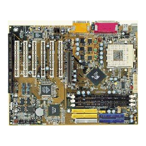
The P6NS PPro SCSI Motherboard is designed with Intel 82440FX PCIset
chipset which is developed by INTEL Corporation to fully support Pentium Pro
Processor PCI/ISA system. The Intel 82440FX PCIset chipset provides increased
integration and improved performance designs. The chipset provides an
integrated IDE controller with two high performanceIDEinterfacesfor up to four
IDE devices (harddevices, CD-ROM device, etc). The Adaptec(AHA-2940UW)
Ultra/ Ultra Wide SCSI built in this SCSI motherboardprovidesnot only the
powerful connectivity but also softwaredriver supported by original Adaptec.
The SMC 37C669 Super I/O controller provides the standard PC I/O function:
floppy interface,two 16 Byte FIFO serial ports and EPP/ECP capableparallel
port. The P6NS layout is shown in next pagefor user's reference. Care must be
taken when inserting memorymodules, inserting Pentium Pro processor CPU or
even plugging PCI card into associated slots to avoid damagingany circuits or
sockets on board.A right fan and heatsink fan isrequired when installing Pentium
Pro processor due to possible overheat.
The P6NS supportsminimum of 8MB of System Memory and maximum of
512MB while L2 Cacheand cache controller included in Pentium Pro Processor .
The P6NS supportsstandard Fast Page, EDO (Extended Data Out or Hyper Page
Mode) or Burst EDO DRAM. The P6NS provides four 72-pins SIMM sites for
memory expansion.The socket support 1M x 32(4MB), 2M x 32(8MB), 4M x
32(16MB), 8M x 32(32MB) 16MB x 32(64MB), and 32MB x 32(128MB)single-
sided or double-sided memorymodules. The memory timing requires 70 nS Fast
page devices or 60 nS EDO DRAM. Memory parity generation and checking or
ECC (Error Checking and Correction) are supported (DRAM Modules may be

9
parity (x 72)or non-parity(x 64)or ECC(x 72). The BIOS will automatically detect
which DRAM hasinstalled in SIMM sites.
The P6NS supportsOnboard two PCI IDE connectors,and detectsIDE
harddisk type by BIOS utility automatically.
The P6NS supports Award Plug & Play BIOS for the ISA and PCI cards. The
BIOS can be located in Flash EPROM. The advantage of having Flash EPROM is
much easier to replace BIOS code if necessary.

10
Placement & Connector
M1
M2
M3
M4
1
Pentium
JP12
CPU
FAN
Speaker
Keylock
Reset SW
SCSI LED
IDELED
SMI SW
Turbo LED
Remote Power On/Off JP7
150
166
180
200
210
233
240
266
270
300 MHz
JP17

11
Jumper Setting
1
Pentium
JP14
JP15
J32
JP18JP11
J
P
16
Power On/Off JP8
JP7
BIOS voltage select
Auto power off JP6
JP5
J33
150
166
180
200
210
233
240
266
270
300 MHz
JP17
JP11 :1-2 Enabled SCSI
2-3 Disabled SCSI
JP16 & JP18 :SCSI Terminator
J33:On Enabled Wide SCSI
Off Disabled Wide SCSI
Remote Control SW Type
J9
:J9 On Normal VGA
Off Diamond VGA
JP1
3.3V from on-board regulator
3.3V from ATX power supply
JP8 :1-2 For Momentary Switch
2-3For Toggle Switch

12
3.3 Block Diagram
Pentium Pro
Processor
Family
MainMemory
BMC
PCIBridge
& Memory
Controller
DBX
Data Bus
Acclerator
MA(11:0)
Control
MD(63:0)
MPE(7:0)
PD(15:0)
Control
PIIX3
I/O Bridge
PCISlots PCI Bus IDE CD-ROM
IDE HDD
HOST Bus
ISA Slots
RTC
BIOS
FlashEPROM KBC
8042
Graphics
Universial
Serial Bus
Port A
Port B
Adaptec
Host SCSI
SCSICD-ROM
SCSIHDD
SCSIDevice
SCSIDevice
For 14 Ultra/Ultra Wide
Internal/ External SCSI Devices

13
3.4 CPU group
The JP17 is a 2 row by 10 line jumperconnector.Only moveone single jumper
cap on this connector.Make sure thespeed that yourCPU really is, or wrong
speed select might cause the system hang.
150
166
180
200
210
233
240
266
270
300 MHz
JP17
3.4.1 Intel Pentium Pro CPU socket
This CPU socket is a 387 pin socket 8. Caremust be taken,When install the CPU
into this socket,. Lift the handlebar,and make sure the CPU pin 1 is with the
squarebase and it goes to particularhole on the ZIF(zero insertion force) socket.
Once you match the hole with the pin 1, then gentle insert the CPU and press
socket handle bar down.
Socket 8
Pin A1
3.4.2 System Memory Configuration
The P6NS supports different type of settings for the system memory.There is no
jumpernor connectorneeded for memory configuration.
M4
M3
M2
M1
Bank 0 Single Side DRAM
Bank 0,1 Dual Side DRAM
Bank 1 Single Side DRAM
Bank 2,3 Dual Side DRAM

14
BANK 0
Socket 1 & 2
BANK 1
Socket 3 & 4
Total Size
4MB x 2
Empty
8MB
4MB x 2
4MB x 2
16MB
4MB x 2
8MB x 2
24MB
4MB x 2
16MB x 2
40MB
4MB x 2
32MB x 2
72MB
4MB x 2
64MB x 2
136MB
8MB x 2
Empty
16MB
8MB x 2
8MB x 2
32MB
8MB x 2
16MB x 2
48MB
8MB x 2
32MB x 2
112MB
16MB x 2
Empty
32MB
16MB x 2
16MB x 2
64MB
16MB x 2
32MB x 2
96MB
32MB x 2
Empty
64MB
32MB x 2
32MB x 2
128MB
32MB x 2
64MB x 2
192MB
64MB x 2
64MB x 2
256MB
128MB x 2
128MB x 2
512MB
NOTE :
1. P6NS supports very flexiblememory configurationswith its 4 SIMM
sockets. The memory size of any configuration can be combined flexibly.
BIOS will detect your memory configurations and sizes automatically.
2. P6NS support Fast Page DRAM, EDO or BEDO DRAM SIMMs, but
cannot be mixed within the same memory bank.
3. SIMMs may be parity (x 72) or non parity (x 64) or ECC(x 72).
4. The 60nS EDO/BEDO DRAM is necessary.
5. The "BANK" means 64 Bit, means either M1+M2 or M3+M4
3.5 Integrated PCI Bridge
The P6NS utilizes Intel's 440FX PCI set chipset to support Pentium Pro

15
Processor PCI/ISA system. The Intel 82440FX PCI set chipset consists of the
82441FX PCI and Memory Controller (PMC), 82442FXData Bus Accelerator
(DBX) devices, and one82371SBPCI ISA/IDE Accelerator (PIIX3) bridge chip.
It provides an interface which translates CPU cycle into PCI bus cycle, and PCI
burst read/write capability. In addition, it provides high performancePCI arbitor
to supportfour PCI Masters, RotatingPriority Mechanism,Hidden Arbitration
Scheme Minimizes Arbitration Overhead,and PCI Rev.2.1 compliant.The PMC
provides bus control signals and addresspathsfortransfersbetween the host bus,
PCI bus, and main memory.The DBX is used to create the 64-bit CPU to main
memory data path and DBX also interfacesto the 16-bit Private data busfor PCI
transactionsand providing optimalCPU-to-DRAM performance.
There are four interrupts in each PCI slot : INTA#, INTB#, INTC#, and INTD#.
Since the P6NS adaptsthe PCI auto-configuration with the system BIOS Setup
utility. When the system is turned on afteraddinga PCI add-in card, the BIOS
automatically configureinterrupts, DMA channels,I/O space,and other
parameters.You do not have to configure jumpers or worry potentialresource
conflicts. BecausePCI cards use the sameinterrupt resource as ISA cards,you
mustspecify the interrupt used by ISA add-in cardsin the BIOS Setup utility.
If however, a "Legacy card" (such as plug paddlecardandcableinto the ISA
slot.) is plugged in the system, modification in the <ROM SETUP UTILITY>
becomesnecessary. First, enter <PCI CONFIGURATION SETUP> utility from
<ROM SETUP UTILITY. main menu to set the <"PCI IDE IRQ MAP TO :
ISA">. Secondly, you must enter <CHIPSET FEATURES SETUP UTILITY>
from <ROM SETUP UTILITY> main menu and set the "<Onboard Primary
PCI IDE: Disabled> and <Onboard Secondary PCI IDE: Disabled>." When
you plug the PCI/ISA IDE card into the system, You should <Disabled Onboard
Primary and Secondary PCI IDE> from <CHIPSET FEATURES SETUP
UTILITY> too.
Some "Legacy card"( no paddle card and cable.) you can set the system interrupt
request (IRQ) on the"Legacy card" (refer to user's manualof the card)to a proper
system IRQ level (in general, card's Primary assigned to INTA and Secondary
assigned to INTB). If the card is plugged into slot 1(marked PCI#1),you can not
use second slot (marked PCI#2) because the Secondary INT signal takesINTB
from the slot (refer to Page 3-12 for circuit diagram).The user then enter <PCI
CONFIGURATION SETUP> utility from <ROM SETUP UTILITY> main
menu and set the "<PCI IDE IRQ MAP TO : PCI-Slot 1>" (depend on the slot
# where the Legacy card is plugged).
3.6 SCSI Interface
3.6.1 J27 Ultra Wide SCSI Connector
J27 is a 68 pins 16 bit internal Ultra Wide SCSI connector. It attachesthe
SCSI cable(s) from this P6NS SCSI controller to theSCSI peripherals.

16
The externalSCSI port expansion kit is a optionalfor your connecting
externaldevices. Be-sure thecable's colored side should align to pin #1 of
this connector.
1
Pentium
P6NS
Ultra SCSI Wide
3.6.2 J26 Ultra SCSI Connector
J26 is a 50 pins 8 bit internal Ultra SCSI connector. It attachesthe SCSI
cable(s) from this P6NS SCSI controller to the SCSI peripherals. The
externalSCSI port expansion kitis a optionalfor your connecting external
devices. Be-sure the cable's colored side should align to pin #1 of this
connector.
1
Pentium
P6NS
50 49
21
3.6.3 Link Internal Ultra & Ultra Wide SCSI devices
The SCSI devices are cabled together in a single, connected series. This
SCSI cablemustrun sequentially from one device to the next,with no
branches.
Table of contents
Other IWILL Motherboard manuals

IWILL
IWILL DN800-SATA User manual

IWILL
IWILL KK266plus-R Original operating instructions

IWILL
IWILL DVD266u-RN User manual

IWILL
IWILL DX400-SN User manual

IWILL
IWILL UPX User manual

IWILL
IWILL DS133R User manual

IWILL
IWILL VD133 Pro Series User manual

IWILL
IWILL P4SE Series User manual

IWILL
IWILL Motherboard DJ800 User manual

IWILL
IWILL dca200 User manual