NXP Semiconductors LPC5410x User manual
Other NXP Semiconductors Microcontroller manuals
NXP Semiconductors
NXP Semiconductors LPC1549 User manual
NXP Semiconductors
NXP Semiconductors TWR-KM34Z50M User manual
NXP Semiconductors
NXP Semiconductors QN9090-DK006 User manual
NXP Semiconductors
NXP Semiconductors S12 MagniV MC9S12ZVML128 User manual
NXP Semiconductors
NXP Semiconductors AN11844 User manual
NXP Semiconductors
NXP Semiconductors LPC86 Series Guide
NXP Semiconductors
NXP Semiconductors ARM Cortex M0+ User manual
NXP Semiconductors
NXP Semiconductors MCUXpresso SDK User manual
NXP Semiconductors
NXP Semiconductors P89LPC9321 UM10310 User manual
NXP Semiconductors
NXP Semiconductors UM11733 User manual
NXP Semiconductors
NXP Semiconductors LPC11E Series User manual
NXP Semiconductors
NXP Semiconductors ColdFire MCF52235 User manual
NXP Semiconductors
NXP Semiconductors i.MX 8M User manual
NXP Semiconductors
NXP Semiconductors QN908 series User manual
NXP Semiconductors
NXP Semiconductors SAFE ASSURE Qorivva MPC5602P User manual
NXP Semiconductors
NXP Semiconductors MTRCKTSPS5744P User manual
NXP Semiconductors
NXP Semiconductors MPC574 P Series User manual
NXP Semiconductors
NXP Semiconductors SLN-LOCAL2-IOT User manual
NXP Semiconductors
NXP Semiconductors UM11527 User manual
NXP Semiconductors
NXP Semiconductors TWR-K60N512-IAR User manual
Popular Microcontroller manuals by other brands
AMS
AMS AS7261 Demo Kit user guide

Novatek
Novatek NT6861 manual
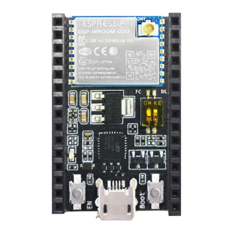
Espressif Systems
Espressif Systems ESP8266 SDK AT Instruction Set
Nuvoton
Nuvoton ISD61S00 ChipCorder Design guide
STMicrolectronics
STMicrolectronics ST7 Assembler Linker user manual
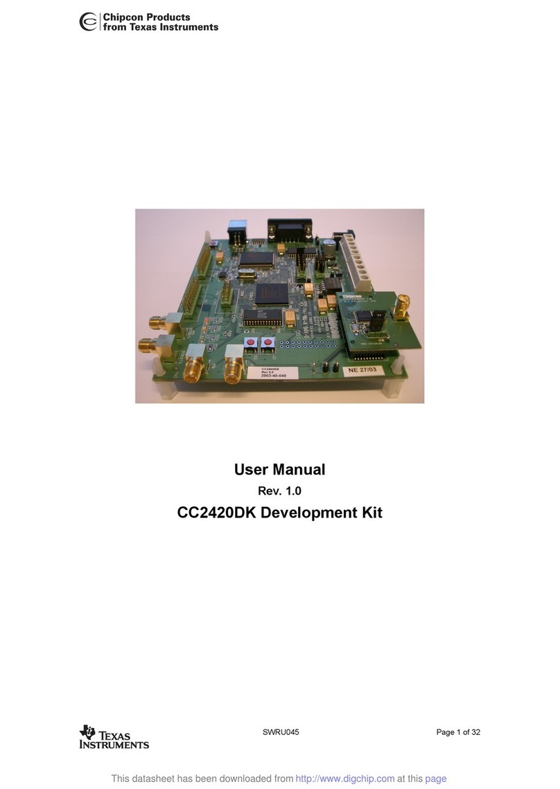
Texas Instruments
Texas Instruments Chipcon CC2420DK user manual

Texas Instruments
Texas Instruments TMS320F2837 D Series Workshop Guide and Lab Manual
CYPRES
CYPRES CY14NVSRAMKIT-001 user guide
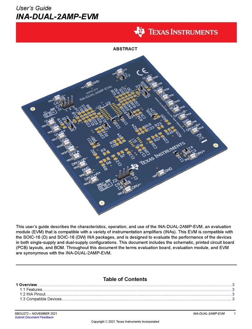
Texas Instruments
Texas Instruments INA-DUAL-2AMP-EVM user guide
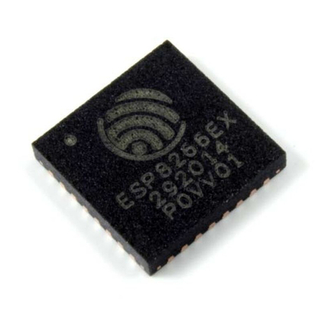
Espressif Systems
Espressif Systems ESP8266EX Programming guide
Abov
Abov AC33M8128L user manual
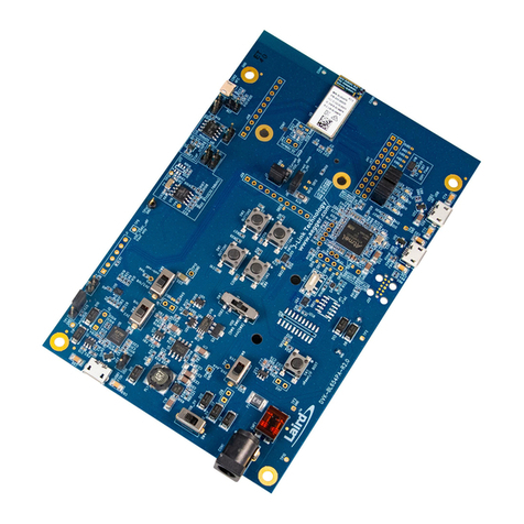
Laird
Laird BL654PA user guide
