K3NC K3NC
4
Specifications
Ratings
Supply
voltage
100 to 240 V
AC (50/60 Hz); 12 to 24 VDC
Operating voltage range
85% to 1
10% of supply voltage
Power consumption (see note)
15 V
A max. (max. AC load with all indicators lit)
10 W max. (max. DC load with all indicators lit)
Sensor power supply
80 mA at 12 VDC
±10%
Insulation resistance
20 M
Ω
min. (at 500 VDC) between external terminal and case.
Insulation provided between inputs, outputs, and power supply
.
Dielectric withstand voltage
2,000 V
AC for 1 min between external terminal and case.
Insulation provided between inputs, outputs, and power supply
.
Noise immunity
±
1,500 V on power supply terminals in normal or common mode
±
1
µ
s, 100 ns for
square-wave noise with 1 ns
V
ibration resistance
Malfunction:
10 to 55 Hz, 0.5-mm for 10 min each in X, Y
, and Z directions
Destruction:
10 to 55 Hz, 0.75-mm for 2 hrs each in X, Y, and Z directions
Shock resistance
Malfunction:
98 m/s
2
(10G) for 3 times each in X, Y
, and Z directions
Destruction:
294 m/s
2
(30G) for 3 times each in X, Y
, and Z directions
Ambient temperature
Operating: –10°
C to 55
°
C (with no icing)
Storage: –20°
C to 65
°
C (with no icing)
Ambient humidity
Operating: 25% to 85% (with no condensation)
Ambient atmosphere
Must be free of corrosive gas
EMC Emission Enclosure: EN55011 Group 1 class A
Emission AC Mains:
EN55011 Group 1 class A
Immunity ESD:
EN61000-4-2:
4-kV contact discharge (level 2)
8-kV air discharge (level 3)
Immunity-RF-interference: ENV50140:
10 V/m (amplitude modulated, 80 MHz to
1 GHz) (level 3)
10 V/m (pulse modulated, 900 MHz)
Immunity Conducted Disturbance:
ENV50141:
10 V (0.15 to 80 MHz) (level 3)
Immunity Burst:
EN61000-4-4:
2-kV power-line (level 3)
2-kV I/O signal-line (level 4)
Approved standards
UL508, CSA22.2; conforms to EN50081-2, EN50082-2, EN61010-1 (IEC1010-1); conforms to
VDE106/part 100 (Finger Protection) when the terminal cover is mounted.
Weight
Approx. 400 g
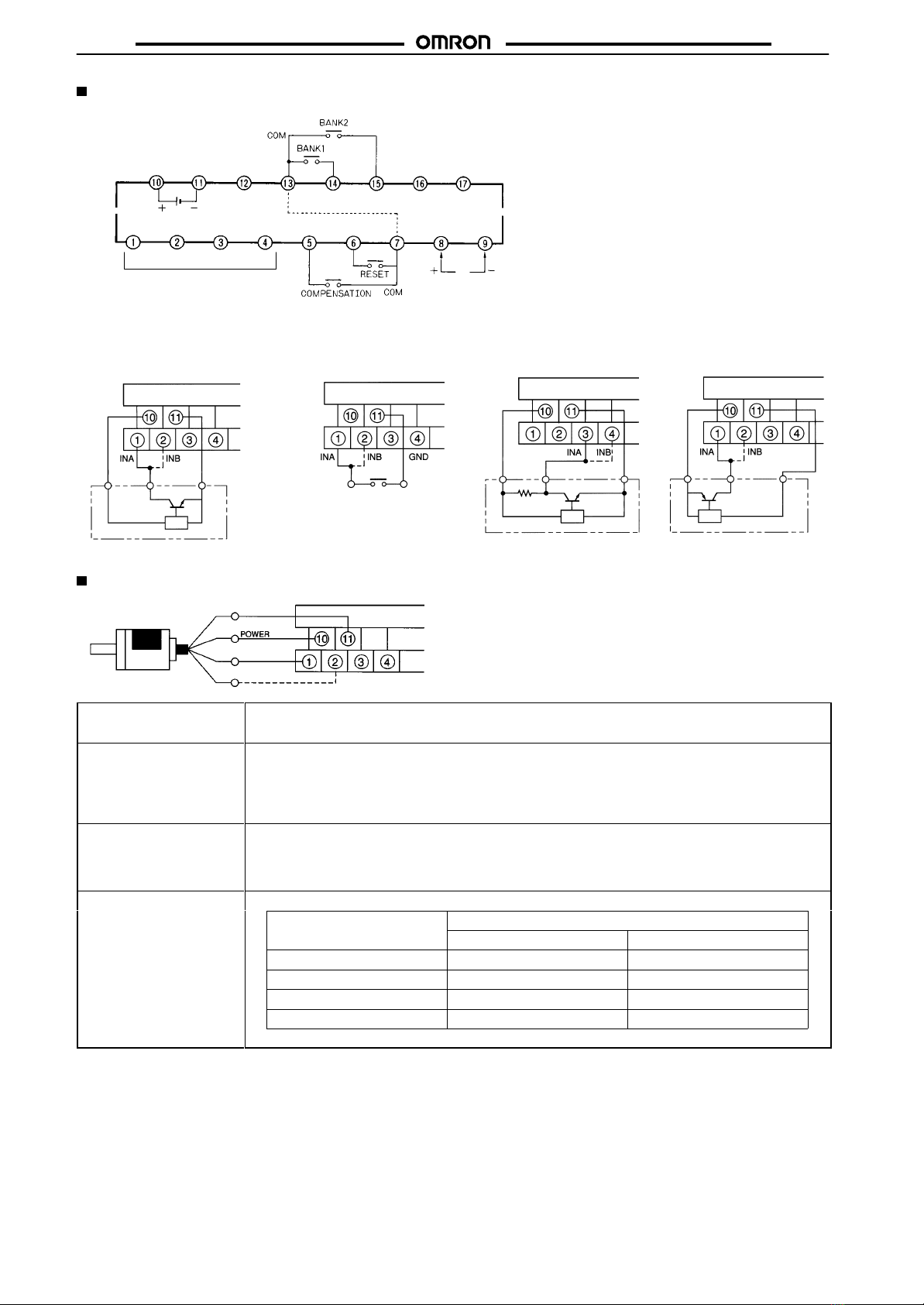
Note: An
Intelligent Signal Processor with DC supply voltage requires approximately 1 A DC as control power supply current the moment the
Intelligent Signal Processor is turned on. Do not forget to take this into consideration when using several Intelligent Signal Processors.
When the Intelligent Signal Processor is
not
in measuring operation (e.g., the Intelligent Signal Processor has been just turned on or is
operating
for startup compensation time), the display will read “
00000
” and all outputs will be OFF
.
Input/Output Ratings
Relay Contact Output
(Incorporating a G6B Relay)
Item
Resistive load (cos
φ
= 1)
Inductive load (cos
φ
= 0.4, L/R = 7 ms)
Rated load
5 A at 250 V
AC; 5 A at 30 VDC
1.5 A at 250 V
AC, 1.5 A at 30 VDC
Rated carry current
5 A max. (at COM terminal)
Max. contact voltage
380 V
AC, 125 VDC
Max. contact current 5 A max. (at COM terminal)
Max. switching capacity
1,250 V
A, 150 W
375 V
A, 80 W
Min. permissible load
(P level, reference value)
10 mA at 5 VDC
Mechanical life
50,000,000 times min. (at a switching frequency of 18,000 times/hr)
Electrical life
(at an ambient temperature of 23
°C)
100,000 times min. (at a rated load switching frequency of 1,800 times/hr)
Transistor Output
Rated load voltage
12 to 24 VDC
+10%/–15%
Max. load current
50 mA
Leakage current
100
µ
A max.