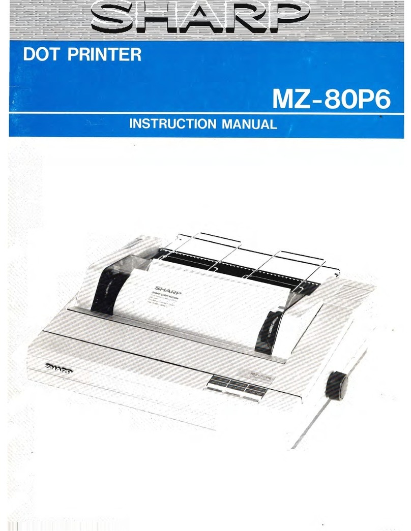
Sharp MZ-80P6 User manual

0
SHARP
• Printing paper
• Character printing
• Bit image printing
•
Paging
• Tabulation
• Feed
• Copies
• Alarm bell
I>f\CIG
2">.1.8~
~
(_o
,
oo
' KU
MA.
''
SERVICE
MANUAL
Dot Printer
MODEL
PDSM881
009-MZ
MZ-80P6
FEATURES
4
to
10
inch
width
fanfold
paper
.and
8.3
to
8.5 inch
width
sheet paper.
Four
character
sizes
are
possible.
Printing
is
possible
with
dot
units.
Number
of
li
nes
printed
on
1
page
can
be
determined.
Both vertical and
horizontal
tabulation
control
is
possible.
,Switch
for
line
by
line paper feed and paper feed
in
page
units.
Control
is
also possible
through
software.
Simultaneous copies,
up
to
3
pages
including
the original,
are
possible.
Alarm
bell sounds
to
warn the user
of
mechanical
trouble,
lack
of
printing
paper, etc.
• Bi-directional printing
Along
with
bi-directional
printing,
there
is
very effective
printing
thanks to
the
use
of
logical seeking.
(Except
for
bit
image
printing
or
for
non
line
• Printing ribbon
space
mode)
lt
can
be
easily
put
in
and taken
out
without
getting ones hands
dirty
because a special cartridge
ribbon
is
used.
SHARP
CORPORAT
·
ION

------
----
Contents-
- -
--
-----
Specifications
Precautions before servicing .
....
.
Explanation
of
MZ-80P6
0 0 0 0 0 0 0 •
Troubleshooting
CPU
board
..
0 0 0 0 0 0 0 0 •
••
•••••••
• 0 • 0 0 0 0 0 0
••
0 0 •
Adjustment
of
head
driving
coil energizing pulse
width
Power
supply
section
...
. .
0 0 0 0 0 •
Functions
of
printer
parts
...
0 • 0 0 • 0 0 0 • 0 0 0 0
•••
Replacing
of
main
printer
parts
0 0
•••••
0 0 0 0 0 0 0 0 •
Replacing
ink
ribbon
from
cartridge
0 0
••••••••
0 0 0
1
2
3
7
15
16
17
22
36
Repair procedure
for
printer
mechanism
0 • • •
•••••••••
0 0 0 0 0 • • • • • • • • • • • • • • • • • • • • • • • • •
39
Circuit
diagram and
printed
wiring
board
0 0 0 0 •
Packing
method
0 0 0 0 0
••••••••
0 0 0 0 0 0
•••
Disassembled views .
0 0 0 0 0 • 0
••••
•
••
0 0 0 • 0
Replacement parts I
ist
.....
0 0 • 0 0
••
•••
••
0
54
60
61
65

SPECIFICATIONS
• General
Item
Specification
Printing
method
Serial
impact
dot
matrix
Feed
method
Variable sprocket feed
or
fric-
tion
feed selectable manually
Kinds
of
characters
I
230 kinds
Character make-
up
I
8(H) x 9(W)
dot
matrix
(normal
size
character)
Line-to-line
space
1/6 inch or determined by pro-
gram
No.
of
digits
Page
Printing
speed
80 digits,
40
digits, 136 digits,
68
digits or determined by program
66 lines/page (line
space
mode)
or determined by program
80 cps (characters per second)
(ordinary
size
characters)
Printing direction
Bi
-
direction
for
I
ine
space
mode
of
character
printing.
Uni-
direction
for
bit
image
printing
and non line
space
mode
of
character printing.
• CPU Board Section
Item
Specifications
CPU
8085A
(Data process
1/
0)
8039P-6 (Step
motor
control)
ROM
2732
*
(8085A
control
and
CG-ROM}
2716
(8039P-6
control
ROM}
1/0
counter
8155
IC
Other IC's 17
Head drive 2SD986 X 8
TR
Step
motor
2SD986 X 8
TR
---
-
Item
Printing paper
Copies
Printing paper
thickness
Ink
ribbon
Head
life
Interface
Specifications
Fanfold
paper
(4-1
0 inch wide}.
Cut
paper sheet
(8.3-8
.5 inch
wide}
Max.
of
3 copies (including
original)
Within
0.3mm
Special cartridge
ribbon
Approx.
50
million
characters (14
dot
character
printing)
8
bit
parallel interface
Power supply
AC
220V
±1
0%
50Hz
AC
240V
± 10%.
50Hz
Power consumption 75W
Working temperature! 5
to
35
°C
Storage temperaturf;)
I
-20
to
50°C
External -dimensions
I
App!fOX.
Weight
377(W}x
352(D)
x 1
05(H)mm
(including
an
assistant guide)
Approx.
7.2
kg
• Power Supply
Unit
Item Specifications
Input
AC
220V
±1
0% 50Hz
AC
240V
±1
0% 50Hz
Output
DC
26V
(21.5
to
26.5V}
DC15V
.
DC
5V
*ROM
2732
(I
C16}
is
not
standard and needs
to
be
ordered separately
because the programs being stored
are
different
by the
computer
to
be
connected.
Types
of
ROM
Host
comput
.er Applicable model
of
ROM
MZ-808
MZ
-8BP5R
MZ-80K
MZ-8KP5R
(Under development}
MZ-80A
MZ
-
8AP5R
(Under development) (Under development)
Note: Specifications and appearance
are
subject
to
change
without
prior
notice
for
improvement. In such a
case,
the explanation here may
be
a
little
different
from
the
product.
-1-
I
PRECAUTIONS BEFORE SERVICING
•
The
printer
mechanism
is
fixed
to
the
chassis
with
four
screws
to
keep
it
from
being
damaged
by
vibration,
etc.
during
transport.
Remove
these
screws
when
using, main-

taining
or
repairing
the
printer.
Fix
the
mechanism
again
with
these
screws
when
transporting
the
printer.
:
111111111
H
0
Il
l0 °
0
111111
111'
11111111111
°
0
Remove the fastening screws
• Do
not
apply
external
force
to
the
print
head,
such
as
by
touching
it
when
it
is
operating.
•
The
print
head
becomes
very
hot
so
do
not
touch
it
with
your
hand
until
it
cools
down
sufficiently.
• Do
not
print
when
the
ink
ribbon
is
loose.
• When servicing
and
checking
a
printer
that
has
been
used
for
a long
time,
remove
dirt,
fuzz
and
dust
from
th~
inside,
and
oil
the
mechanism.
•
There
are
two
types
of
oil,
G2
and
02.
Use
the
proper
oil
for
each
oil
point.
(Refer
to
page
63,
64
for
oil
points.)
•
There
are
screws
and
nuts
which
are
fixed
and
then
locked
with
paint
for
vibration-
proof
etc.
during
transport.
Paint
the
screws
to
lock
them
after
disassembling
and
replacing
new
parts.
(Refer
to
page
63,
64
for
the
pointsto
be
painted
to
lock
the
screws.)
•
To
hold
the
printer
mechanism
only,
hold
at
the
points
illustrated
below.
Especially
do
not
hold
the
paper
sensing device
and
the
paper
guide
section.
-2-

EXPLANATION
OF
MZ-80P6
• Construction
Model MZ-80P6 consists
of
a locig
1,
logic
2,
print
head driver,
motor
driver,
printing
mechanism,
control
switches,
and power supply,
as
illustrated below.
Control
switches
Printing
mechanism
~--------·
I
Logic
1 I
(8085)
Print
head
driver
I
Print
head
I
I
I I
I
Timing
belt
motor
Logic
2 I
(8039)
Motor
driver
I
'
I
Paper
feeding
motor
I
I
I
Sensor I
I
L._
________
....J
• Explanation
of
Logics
and Drivers
1. Block diagram
The
printer
employs
two
microprocessors,
8085
and 8039. The
former
is
primarily
used
for
data process and
print
head
control,
and the
latter
for
stepping
motor
control
and
control
switch
input
process. Employed external
ROM's
are
2732
and 2716. The
former
stores processing programs and condensed characters
for
the micro-
processor 8085, and the
latter
processing programs
for
8039.
The
8155
is
a
RAM
with
1/0
ports and
counter/timer
and
used
in
conjunction
with
the 8085. Its capacity
is
256 bytes
of
which
136
bytes
are
used
for
storing data and the rest
for
a
work
area. The
1/0
ports
are
connected
to
the parallel interface,
print
head drive
circuit,
control
bus
to
the 8039, and display
circuit.
The
8039
incorpo-
rates
1/0
ports and
RAM
(128 bytes), and connected
to
the stepping
motor
drive
circuit,
external sensor
circuit,
and
control
bus
from
the 8085,
through
the
1/0
ports. The
RAM
is
used
as
a
work
area.
Interface
(Option
terminals)
STATUS
Print
head
drive
circuit
IRT
-3-
Motor
drive
Sensor
circuit
8039
CPU,
RAM
,
1/0
PORT
~
Power
supply
I

2. Reset circuit
(1)
At
switching
on
of
power
supply
The
circuit
forms
a
reset
signal
by
making
use
of
a
charging
time
of
a
resistor
R
17
(10KS1)
and
a
capacitor
C9
(47pF)
and
resets
IC13
8085,
IC12
8155,
and
IC21
8039.
+5V
ISI~§
4
f
Rl7
IC5
RIG
IOK
LSI4
IOOlt
13
CLAMP'
......
~~ilv,......_+-~
ll
~
,.+
I
C5
il~C9
IOOOP
,..,47)l/16V
(2)
At
momentary
interruption
and
turning
off
of
power
supply
IC5
LS14
12
3
Z2
RESET
+5V
-
---:~"
Leading edge
of
/
/
/
/
power
supply
1
~i=::::::!..._
____
_
Reset signal
If
+5V
power
supply
is
reduced
below
approx.
4V,
the
clamping
circuit
is
actuated
to
form
a reset signal.
Whereby,
all
the
circtJits
are
reset
at
momentary
power
supply
interruption
to
protect
the
programs
and
drive
circuits
from
the
voltage
drop
of
the
+5V
line.
When
the
power
supply
is
turned
off,
a reset signal
is
generated
at
the
same
time
of
interruption
to
protect
the
drive
circuits
from
faulty
operation
due
to
the
residual
voltage
determined
by
the
time
constant
of
the
power
supply.
+15V
+5V-v-
~~-.-.-=-.-.-.-.~CL~.-.-.-~r-.-.-.-~
+5V
I
8085
®
Pin
V:1V/div
H:20msec/div
8085
@ Pin V:
1V/div
H:5msec/div
Reset
signal
waveform
at
power
supply
switching
on
Reset
signal
waveform
at
power
supply
switching
off
3.
8155
(256 bytes RAM, with
1/0
ports and timer)
136
bytes
of
the
RAM in
the
8155
are
used
for
the
character
code
storage
area
of
one
line
character
codes
and
the
rest
for
a
working
area.
Data
(RD
1
to
RD
8)
from
the
parallel
interface
is
input
from
the
1/0
ports
(PA
0
to
PA
7)
and
stored
in
the
accu-
mulator
of
the
8085
where
it
is
identified
whether
the
data
is
character
data,
control
code,
code
other
than
those
listed in
character
code
table,
or
image
print
data.
If
the
data
are
character
data,
they
are
stored
in
the
above
mentioned
RAM
up
to
one
line.
When
one
line
data
are
accumulated,
the
8085
reads
dot
patterns
cor-
responding
to
the
character
data
from
the
character
generator
(2732)
and
outputs
the
pattern
to
the
PBo
to
PB1
of
the
8155.
With
the
image
print
data,
they
are
not
stored
in
the
RAM
but
are
output
to
PBo
to
PB1
in
every
one
piece
of
data.
When
character
printing
data
are
input
and
being
printed,
an available
space
is
judged
and
the
bi-directional
shortest
printing
is
made.
In
the
image
printing
and
the
condensed
mode,
the
mono-directional
quick
return
printing
is
employed.
The
8155
has also a
function
of
the
timer
and
the
timing
of
half
dot
is
formed
by
receiving
clock
signal (2MHz)
from
the
8039.
-
PC
o PAo
RDA
-
STATUS
RD
l
PC1
~
)
8039
p24
PC
2
DOT
TIMING
PC3
RDs
PA7
ONLINE
LED
PC4
POWER
LED
PCs
PB
o
FROM8039
\
PIN1
2MHz
TIMER
IN
s
PINS
To
8085
RST7.5
TIMER
OUT
PB7
8155
-4-

4.
8039
(CPU with
128
bytes
RAM
and
1/0
ports)
The
8039
is
used
primarily
for
controlling
the stepping
motor.
lt
outputs
control
signals
from
P
1 0
to
P
1 7 •
PM
1A and
PM
1
Bare
a
driving
pulse
of
the
timing
belt
motor,
and HOLD1 and HO
LD2
control
the
timing
belt
motor
to
select normal characters (80 characters/line)
or
condensed characters (136 characters/line).
PM2A,
PM2B, and
HOLD3
control
the paper feeding
motor.
These
functions
are
generated
by
decoding
control
data
from
the
8085,
input
to
D8
0
to
DB
7.
Signals
for
data
communication
between
8085
and
8039
are
input
to
and
output
from
P2
4
(from
8155
PC
2)
and
P2
7
(8039
READY).
Square wave
of
2KHz
for
signaling the buzzer
is
output
from
P
1 7 .
DB
o Pto PM1A
P11
PM1B
DB
7
P12
PM2A
A
s
~
P
20
Pt3 PM2B
I t
P1
4
At
o P
22
HOLD1
FROM
8155PC2
P24
Pts
HOLD2
FEED
SW
P
25
Pt
6 HOLD3
T.O.F
SW
P
26
p17
BUZZER
8039R
EADY P
27
5. Print head drive circuit
If
dot
pattern
and
dot
timing
pulse are
output
from
I
/0
port
IC8155, electric
current
flows
through
the
print
head.
Dot
timing
pulse triggers
the
555
through
a
circuit
for
generating
short
duration
pulse
to
produce
print
head drive pulse
of
400J,lsec (at a power supply voltage
of
24V)
. The
print
head drive pulse
is
pulse-duration
modulated
with
a
power
supply
voltage
of
26V
(the pulse-duration
is
reduced at high
power
supply voltage and
increased at
low
voltage), and
the
energy supplied
to
the
print
head
is
whereby constant.
r -- -
Print
head
drive pulse
generator-
,----
- -
016
2SD986
-
"""2"
sv
-
I
CCN2)
I
f
I
I
PIN I
Br:5..5P<3
I
DOT
T
I
M
IN
~
PULSE
Z07
R
26
0525.6
68
0/2W
~
26v
RES
IC
3
I
-
C21
T062504P
I
0
OUJ
l
____
_
-,
I
Circuit
forming
pulse
of
short
duration
1
I
I
201<
R25
151<
Cl9
IOQOP
PIN 3
PIN
4
PIN
5
PIN
7
PIN
8
3.3)(
(RA2 3.
31<
xSl
I
I
I
I
L _ _
__
_
--
--
----
-- -
----_
I_.
-----
L
--
-
--
-
Print
head
drive
circuit----
-
_J
lll
r
ii
JMf
V :1V
/div
H:
500J.,Lsec
/d iv
Waveform
(at
test
printing)
at
555
®
pin
r- r-
r-
r--
~
---
'--
_
:___
__
--
V :1V /
div
H:
500J.,Lsec
/
div
Waveform
at
test
point
(at
test
printing)
-5-
1
.\
~
\.
f'-
I I
I
I
V :1
OV
/div
H :500J.,Lsec/div
CN2G)to@terminals
(at
test
printing)

6. Timing
belt
motor
drive
circuit
When
HOLD1
signal
is
low
and
HOLD2
signal high, the
018
2SB743
is
turned
on and the
019
2SB743
is
turned
o~f
to
pass
+26V
current
through
the stepping
motor.
In this
case,
the mode
is
SO-characters/line.
Contrarily,
when
HOLD1
signal
is
high and
HOLD2
signal
is
low,
current
of
+15V
flows and the mode
is
136-characters/
line. In
both
modes, the
print
head
is
driven
from
left
to
right,
or
vice
versa
by
transmitting
motor
drive sequence
pulse
to
PM1A
and
PM1
B.
If
both
HOLD
1 and
HOLD2
signals
are
turned
high,
both
018
and
019
are
turned
off
and a
holding
current
flows
through
the stepping
motor
through
the
R2
(120f2/5W). The
intention
of
the
holding
current
is
to
prevent
the step-out
of
the stepping
motor
due
to
vibration
etc.
while
the stepping
motor
is
standing still.
\J.
N \
1\ \ \
--
r-
-
V:10V/div
H:2msec/div
CN2@
to
@terminals
(At
test
printing)
7. Paper feeding
motor
drive
circuit
When
HOLD3
signal turns
low,
the
017
is
turned
on
to
pass
a
current
of
+26V
through
the stepping
motor.
In this situation, paper
is
fed
by
transmitting
motor
drive sequence pulse
to
PM2A
and PM2B. When HO
LD3
signal
is
high, a
holding
current
is
passed
through
the R1 (
120f2/5W).
~
~
~
r\
.\
.\ \
"
r-.,
\.:,
I I
r------
---------------
-~
I I
...
-
...
~
-I +
15V
I
I I
I
1
I
I
HOLD 2
I
I I
I I
V:10V/div
H:5msec/div
CN2
@
to
@
terminals
(At
test
printing)
r--------
---
I
- - --
:6~
-:5
:-
-
-l
:
HOLD 3
---'=Q
HOLD
I
I
I
I
I
I
I
1>"'---<..._-/~5~+--+---+---28
I
24---11---+--+---.<~1---+---'~
P.:...-.!::.OC
I
I
I
I
ICIB
LS04
ICI
LSO!S
D8
5!12778
Paper
feeding
motor
drive
circuit
I
Timing
belt
motor
drive
circuit
_L
__________________
_ _
-6-

T·
ROUBLESHOOTING
CPU
BOARD
NO
NO
NO
NO
NO
NO
NO
NO
Go
to
"CHECK
OF
POWER
SUPPLY
CIRCUIT".
Go
to
"CHECK
OF
TIMING
BELT
MOTOR
CIRCUIT".
Go
to
"CHECK
OF
LED
CIRCUIT".
Go
to
"CHECK
OF
SW
CIRCUIT".
Go
to
"CHECK
OF
LINE
FEED
CIRCUIT"
.
Go
to
"CHECK
OF
TOP OF
FORM
CIRCUIT"
.
cGo
to
"CHECK
OF
PRINT
HEAD
DRIVE
CIRCUIT"
. )
Go
to
"CHECK
OF
TIMING
BELT
MOTOR
CIRCUIT".
Go
to
"PAPER
FEEDING
MOTOR
DRIVE
CIRCUIT"
.
Go
to
"CHECK
OF
PRINTER
INTERFACE
CIRCUIT".
Che
ck
interfac
e cards.
OK
-7-

Refer
to
waveform
(Page
6).
CHECK
OF
TIMING
BELT
MOTOR
CIRCUIT
YES
Check
timing
belt
motor
.
NO
NO
NO
NO
NO
NO
-8-
Check
8039
circuit.
Check IC2, IC6, and
surrounding
circuits.
Check
018
and
020
.
Check
8039
circuit.
Check IC2 and IC18.
Check
01
to
04.
74LS05
TD62003P
2S8743
S5277B
74LS05
74LS04
2SD986

CHECK
OF
LED
CIRCUIT
CHECK
OF
SW
CIRCUIT
No
NO
NO
-9-
Check
8085
circuit.
Check
pattern.
Check IC6.
TD62003P
Check
LED
SW
circuit.
Check
8085
circuit.
Check
chip
select
circuit
.
Check IC9.
Check IC15.
74LS32
74LS244

CHECK
OF
PAPER
FEEDING
MOTOR
DRIVE
CIRCUIT
Check
LED
SW
board.
Check R30, R33,
and C25.
Check IC19.
TC40H004P
Check
8039
circuit.
Check IC1, IC6, and
surrounding
circuits.
Check
017
and D18.
Check
8039
circuit.
Check
IC1
, and IC18.
Check
05
to
08.
Check paper feeding
motor.
-10-
CHECK
OF
TOP
OF
FORM
CIRCUIT
Check
LED
SW
board.
Check
R29
, R32, and C24.
Check IC19.
74LS05
TD62003P
2SB743
S5277B
74LS05
74LS04
2SD986

555
YES
Check
print
head.
Check
8085
circuit
.
Check reset
circuit.
Check
timing
pulse
generator
circuit.
Check
IC19
and
~
.
surrounding
circuits.
555
Check
IC3 and
021.
TD62504P
2SA1015
Check
8085
circuit
.
Check
09
to
016
.
2SD986
-
11
-
Connect
cable.
Check IC11.
74LS244
Check
IC10
.
75189
Check
8085
circuit
.
~
CheckiC3.
TD62504P
Check
8085
circuit.
Check
IC3.
TD62504P

ASSOCIATION
WITH
B039
CIRCUIT
8039
Check
reset
circuit.
Check
oscillator
circuit.
Correct
and
back
to
"START"
step.
Check
IC21.
8039
Check
IC18
or
pattern
discontinued.
74l
~:
S04
Check
IC20
.
2716
Check IC21,
or
pattern
touch.
Correct
and back
to
"START"
step.
Correct
and
back
to
"START"
step.
-12-
CHECK
OF
8085
CIRCUIT
Check
of
ROM
(2732)
Check
of
8155
Check
of
IC15
74LS244
Check
oscillator
circuit.
Check reset
circuit.
GJi'eck
R44.
Check
pattern.
Check
pattern
.
Check
each bus
line
.

CHECK
OF
ROM
Check
chip
select
circuit.
Check IC5.
74LS14
Check
R31.
Check
IC14.
74LS273
Check bus lines.
Check
bus lines.
2732
-13-
CHECK
OF
8155
Check
pattern.
Check
IC5.
74LS14
Check bus lines.
8155
Check 1C12.
8155
Check IC12.
8155
Check
IC12.
YES
OK

CHECK
OF
IC15
74LS244
Check
eh
ip
select
circuit.
Check
pattern.
Check IC9.
74LS32
Check IC15.
74LS244
-
14-
CHIP
SELE<;:T
CIRCUIT
Check IC9.
74LS32
Check bus lines.
Check IC8.
74LS42
YES
OK

ADJUSTMENT OF
HEAD
DRIVING COIL ENERGIZING PULSE WIDTH
This
concerns
the
printing
energy
force
for
the
head
wire
to
print
a
dot
and
its
length
in
time
as well.
The
shorter
the
energizing
pulse
width
(time)
is,
the
smaller
the
printing
energy
is,
thus
weakening
printed
letters.
To
the
contrary,
the
larger
pulse
width
prolongs
the
printing
time
of
head
wire,
thereby
feeding
the
head
with
the
head
wire
clacking
out.
In
most
cases,
the
head
wire
is
caught
by
the
ink
ribbon,
and
what
is
worse,
the
tip
of
head
wire
is
broken.
This
adjustment
is
required
to
give
an
appropriate
printing
energy
to
the
head
wire.
Make an
adjustment
in
the
following
manner.
1)
Remove
upper
cabinet.
(Do
not
disconnect
the
connector
of
on/off
line,
top
of
form
and
line
feed
switch
circuit.)
2)
Take
out
the
head
cord
PWB
connecto
r
from
the
connector
of
terminal
PWB.
Be
careful
not
to
damage
the
head
cord
PWB.
3)
Turn
on
the
paper
end
sensor.
(Put
a
piece
of
paper
in
the
paper
sensor
lever
located
at
printing
paper
insertion
area.)
4)
Draw
out
the
power
supply
socket
(CN4)
with
5-pin
lead
from
the
CPU
board.
5)
Connect
3
units
of
D.C.
power
supply
to
the
5-
pin
connector
(CN4)
of
CPU
board
as
shown
below:
24V
D.
C.
(current
capacity:
1.5A
or
more),
14V
D.C.
and
5V
D.C.
6)
While
pushing
the
line
feed
switch
of
the
set
turn
on
the
power
switches
of
the
three
D.C
.
power
supply
units.
(The
head
is
shifted
right
and
left.)
7)
Connect
the
synchroscope
to
the
test
point
which
is
connected
to
the
collector
of
the
transistor
021
(2SA
1
015)
on
the
CPU PWB
to
check
to
see if
the
pulse
width
on
the
synchroscope
is
400
±10 11sec.lf
the
width
i~
out
of
standard
value,
rotate
the
semi-variable
resistor
(VR1)
at
the
CPU PWB
to
adjust
the
width.
(The
semi-variable
resistor
is
to
be
fixed
with
lacquer
after
adjustment.)
Note:
Before
checking
pulse
width,
calibrate
the
synchroscope
to
eliminate
error
in
time
base.
~400±1
0
J1Sec
~
Head
driving
coil
energizing
pulse
signal
24V
(Current
capacity:
1.
5A
or
more)
For
pulse
width
adjustment
---8
G-
---8
--8
G-
---8
c::=:::J
--E.)
c::=:::J
---8
c::=:::J
IC3
-E)
c::=:::J
u
~
[)
-E)c=:J
-B
G-
~
6
~
~
·~
I0 n
IC8
-E)
c=:J
--E)
CJ
=§
©
G-
--E.)
[:=::::J 0
--f)
r=:J
0
p
'm
-E)
c:=J
cb
p
ICS
I
IC9
G-
--E)
c::::::J
Connecting
diagram
for
power
supply
and
synchroscope
-15-

POWER SUPPLV SECTION
• Block Diagram of Power Supply Circuit
~
Rectifier
Smoothing
section section
-
ACI
NPUT
Filter
Power
Rectifier
Smoothing
o-
-=-
section
transformer
section section
f--
~
Rectifier
Smoothing
section section
• Troubleshooting
NO
NO
NO
YES
NO NO
YES
NO
NO
YES
-16-
-
Regulator
{)
section
+26V
(21.5
""26.5V)
Regulator
------<>
section
+5V
Regulator
0
section
+15V
Check
power
transformer
and
input
circuit.
Check
80103,
F1
03,
C1
03,
C1
04.
CheckR101,
Z01
02,
0102.
Check0101,
output
connector
Check
80102,
F104,
C105
Check
IC1
02,
output
connector
Check
80101,
F1
05,
C106.
Check
IC101
output
connector

FUNCTIONS
OF
_PRINTER
~
PARTS
•
Exterior
of
Mechanism
and
Names
of
Parts
Release lever
Adjusting
lever
Sprocket
unit
Paper
feeding
motor
Timing
belt
motor
•
Sensing
Mechanisms
Sensing
mechanisms
consist
of
HP
sensor,
PTS
sensor
and
PE
sensor.
The
HP
sensor
is
attached
to
determine
the
Home
Position
of
the
carriage
and
generates
the
reference
signal
for
printing
.
The
PTS
sensor
generates
the
timing
signal
used
to
determine
printing
position.
lt
detects
this
signal
and
adjusts
carriage
speed.
The
PE
sensor
detects
the
presence
or
absence
of
paper.
1.
HP
Sensor (Home Position Sensor)
The
HP
sensor
consists
of
the
home
position
sensor
assembly
anq
sensor
board
on
the
lower
part
of
the
carriage.
The
signal
is
High
when
the
sensor
board
interrupts
the
light
shaft
of
the
photo
coupler.
(lt
is
an
open
collector
output)
-17-

2. PTS Sensor (Print Timing Signal Sensor)
The
PTS
sensor
consists
of
the
PTS
sensor
board
assembly
and
the
sensor
board
on
the
timing
belt
motor
shaft.
The
signal
is
Low
when
the
slit
of
the
sensor
board
appears.
(lt
is
an
open
collector
output.)
3. Paper Sensor
The
paper
sensor
consists
of
the
reed
switch
attached
to
paper
sensor
board
and
the
permanent
magnet
attached
to
the
paper
sensor
lever.
The
permanent
magnet
approaches
the
reed
switch
and
the. signal passes
when
there
is
no
paper.
4. Sensor Circuit
To
+5V
HP
signal Paper sensor
Reed
switch
o----o~
PTS signal
~Permanent
magnet
To
GND
• Printing Mechanism
The
main
elements
of
the
pnntmg
mechanism
are
print
head
unit,
carriage,
t1m1ng belt,
timing
belt
motor
and
platen.
The
print
head
unit
on
the
carriage
is
moved
to
the
right
and
left
by
the
timing
belt
on
shafts
A
and
B
of
the
carriage guide.
The
timing
belt
is
driven
by
the
timing
belt
motor
through
the
belt
driving
pulley
and
belt
driven
pulley.
Printing
performs
when
the
dot
wire
springs
out
toward
the
platen
due
to
the
flow
of
current
in
the
head
driving
coil.
The
current
flows
when
the
PTS signal
is
generated
by
the
belt
motor
rotation.
Carriage
drive
signal
HP signal
I......____--..Jr-
1
--------2-.5-4_m_m_(-1/_1_o·-·
)
---------(~
$\---
PTS signal
-
f-
Head
drive
coiI signal
=fl--
·2.08ms
0.4ms
-----'
Dot
wire
tip
----~~------
1. Principle
of
Carriage Movement
The
carriage
is
moved
to
the
right
and
left
by
the
drive
of
the
timing
belt
motor
with
the
timing
belt
inserted
in
the
carriage.
Carriage
Timing
belt
motor
Junction
Left
Right
Timing
belt
-18-
Other manuals for MZ-80P6
1
Table of contents
Other Sharp Printer manuals

Sharp
Sharp AR-M351N User manual

Sharp
Sharp SX 1075 User manual

Sharp
Sharp CE-126P User manual

Sharp
Sharp DP-750 User manual

Sharp
Sharp MX-C407P User manual

Sharp
Sharp AR-M351N User manual

Sharp
Sharp MX-B467P User manual

Sharp
Sharp AR-C200P - Color Laser Printer User manual

Sharp
Sharp AJ-1805 Setup guide

Sharp
Sharp CE-150 User manual

Sharp
Sharp AR-M450 Imager User manual

Sharp
Sharp DX-B350P User manual

Sharp
Sharp SD-2060 User manual

Sharp
Sharp AR-M208 User manual

Sharp
Sharp JX-9500E User manual

Sharp
Sharp AJ-6110 Setup guide

Sharp
Sharp MX-C300P User manual

Sharp
Sharp AR-PE2 User manual

Sharp
Sharp DX-B350P User manual

Sharp
Sharp AR-M280 User manual