manuals.online logo
Brands
  1. Home
  2. •
  3. Brands
  4. •
  5. Sony
  6. •
  7. Computer Hardware
  8. •
  9. Sony CMOS CXP854P60 User manual

Sony CMOS CXP854P60 User manual

Description
The CXP854P60 are a highly integrated micro-
computers composed of a 8-bit CPU, PROM, RAM,
and I/O ports. These chips feature many other high-
performance circuits in a single-chip CMOS design,
including an A/D converter, serial interface,
timer/counter, time-base timer, vector interrupt, on-
screen display function, I2C bus interface, PWM
generator, remote control receiver, HSYNC counter,
and watchdog timer.
Also, the CXP854P60 provides power-on reset
and sleep functions. The designers have ensured
low power consumption for these powerful micro-
computers.
Incorporating a one-time PROM, the CXP854P60
has an equivalent function to the CXP85460 and
character ROM for OSD can be written. Therefore, it
is suitable for evaluation in system development
and for the production of small amounts.
Features
•Instruction set which supports a wide array of data types-213 types of instructions which include 16-bit
calculations, multiplication and division arithmetic, and boolean operations.
•Minimum instruction cycle 0.5µs/8MHz
•On-chip PROM 60K bytes (For program)
10K bytes (For OSD)
•On-chip RAM 960 bytes
•On-screen display function 12 ×18 dots, 384 types, 12lines of 32 characters
Black frame output, half blanking, shadow, background color on full screen
Double scanning mode supported includes jitter elimination circuit
•I2C bus interface
•14-bit PWM output, 8-bit PWM output (8 channels)
•Remote control receiver circuit
•8-bit A/D converter (4 channels, 20µs conversion time/4MHz, 8MHz)
•HSYNC counter (2channels)
•Watchdog timer
•8-bit synchronized serial I/O
•8-bit timer, 8-bit timer/counter, 19-bit time-base timer
•General purpose input/output 32-line I/O (bit-selectable input/output), also 6-line input, 10-line output (internal
8-line Nch-O/D)
•Interrupts 13 factors, 13 vectors, multiple interrupt possible
•Standby mode SLEEP
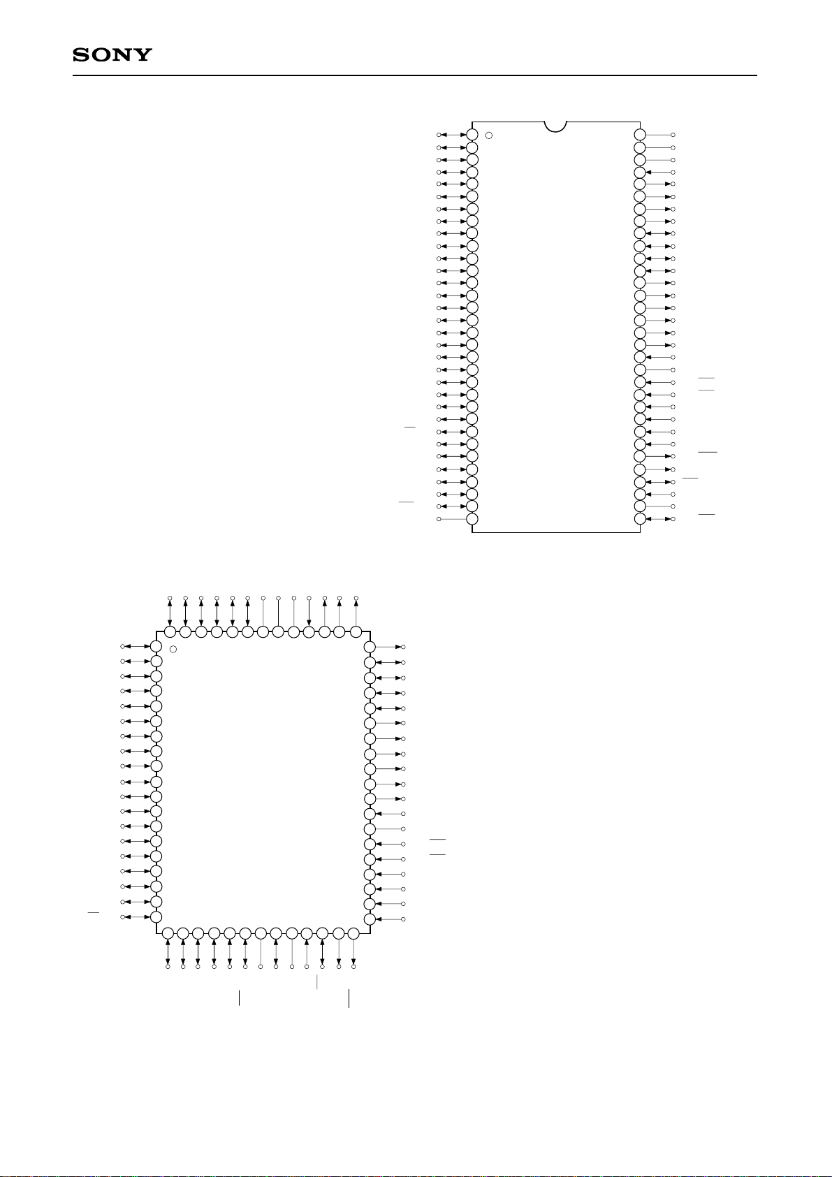
•Package 64-pin plastic SDIP/QFP
Purchase of Sony's I2C components conveys a license under the Philips I2C Patent Rights to use these components
in an I2C system, provided that the system conforms to the I2C Standard Specifications as defined by Philips.
– 1 –
CXP854P60
E95109A16-PS
CMOS 8-bit Single-chip Microcomputer
Sony reserves the right to change products and specifications without prior notice. This information does not convey any license by
any implication or otherwise under any patents or other right. Application circuits shown, if any, are typical examples illustrating the
operation of the devices. Sony cannot assume responsibility for any problems arising out of the use of these circuits.
64 pin SDIP (PIastic) 64 pin QFP (PIastic)
Structure
Silicon gate CMOS IC
– 2 –
CXP854P60
ON SCREEN DISPLAY
SERIAL I/O
TIMER/COUNTER
REMOCON FIFO
A/D CONVERTER
I2C
INTERFACE UNIT
WATCH DOG TIMER
14BIT PWM 8 BIT PWM
8CH
CLOCK GEN./
SYSTEM CONTROL
RAM
960 BYTES
SPC700
CPU CORE
PROM
60K
PRESCALER/
TIME BASE TIMER
PORT A
PORT B
PORT C
PORT D
PORT E
PORT F
2
2
V
SS
V
DD
MP
RST
XTAL
EXTAL
PD0/INT2
PE1/INT1
PE0/INT0
PF0/PWM0
to
PF7/PWM7
INTERRUPT
CONTROLLER
PE6/PWM
PA0 to PA7
PB0 to PB7
PC0 to PC7
PD0 to PD7
PE0 to PE5
PE6 to PE7
PF0 to PF7
XLC
EXLC
R
G
BI
YS
YM
PA7/HSYNC
PA6/VSYNC
PD3/SI
PD2/SO
PD1/SCK
PD7/EC
PE7/TO
PD6/RMC
PD4/HS0
PD5/HS1
PE2/AN0
to
PE5/AN3
PF4/SCL0
PF5/SCL1
PF6/SDA0
PF7/SDA1
HSYNC COUNTER 0
HSYNC COUNTER 1
Vpp
Block Diagram
–3 –
CXP854P60
HSYNC/PA7
VSYNC/PA6
PA5
PA4
PA3
PA2
PA1
PA0
PB7
PB6
PB5
PB4
PB3
PB2
PB1
PB0
PC7
PC6
PC5
PC4
PC3
PC2
PC1
PC0
EC/PD7
RMC/PD6
HS1/PD5
HS0/PD4
SI/PD3
SO/PD2
SCK/PD1
VSS
VDD
Vpp
VSS
MP
PF0/PWM0
PF1/PWM1
PF2/PWM2
PF3/PWM3
PF4/PWM4/SCL0
PF5/PWM5/SCL1
PF6/PWM6/SDA0
PF7/PWM7/SDA1
YM
YS
I
B
G
R
EXLC
XLC
PE0/INT0
PE1/INT1
PE2/AN0
PE3/AN1
PE4/AN2
PE5/AN3
PE6/PWM
PE7/TO
RST
EXTAL
XTAL
PD0/INT2
2
3
4
5
6
7
8
9
10
11
12
13
14
15
16
17
18
19
20
21
22
23
24
25
26
27
28
29
30
40
39
38
37
36
35
34
31
32 33
41
42
43
44
45
46
47
48
49
50
51
52
53
54
55
56
57
58
59
60
63
64
61
62
1
Pin Assignment (Top View)
2
3
4
5
6
7
8
9
10
11
12
13
14
15
16
17
18
19
20 21 22 23 24 25 26 27 28 30
40
39
38
37
36
35
34
31 32
33
41
42
43
44
45
46
47
48
49
50
51
52
53
54
55
56
57
58
59
60
63
64 61
62
1
PA1
PA0
PB7
PB6
PB5
PB4
PB3
PB2
PB1
PB0
PC7
PC6
PC5
PC4
PC3
PC2
PC1
PC0
EC/PD7
PF3/PWM3
PF4/PWM4/SCL0
PF5/PWM5/SCL1
PF6/PWM6/SDA0
PF7/PWM7/SDA1
YM
YS
I
B
G
R
EXLC
XLC
PE0/INT0
PE1/INT1
PE2/AN0
PE3/AN1
PE4/AN2
PE5/AN3
RMC/PD6
HS1/PD5
HS0/PD4
SI/PD3
SO/PD2
SCK/PD1
VSS
INT2/PD0
XTAL
EXTAL
RST
TO/PE7
PWM/PE6
PA2
PA3
PA4
PA5
PA6/VSYNC
PA7/HSYNC
VSS
VDD
Vpp
MP
PF0/PWM0
PF1/PWM1
PF2/PWM2
29
Note) 1. Vpp pin 63 must be connected to VDD.
2. Vss pins 32 and 62 must have a common GND.
3. MP pin 61 must be connected to GND.
Note) 1. Vpp pin 56 must be connected to VDD.
2. Vss pins 26 and 58 must have a common GND.
3. MP pin 55 must be connected to GND.
–4 –
CXP854P60
(Port A)
Single bit selectable 8-bit port.
(8 lines)
(Port B)
Single bit selectable 8-bit port.
(8 lines)
(Port C)
Single bit selectable 8-bit port.
(8 lines)
(Port D)
Single bit selectable
8-bit port.
12mA sink current
drive possible.
(8 lines)
(Port E)
8-bit port, lower
6 bits for input,
upper 2 bits for
output.
(8 lines)
(Port F)
8-bit output port
with large current
(12mA) N-ch open
drain output.
Lower 4 bits middle
voltage tolerance
(12V), upper 4 bits
5V suppression.
(8 lines)
CRT display 6-bit output pin.
Pin Functions
Pin Name
PA0 to PA5
PA6/VSYNC
PA7/HSYNC
PB0 to PB7
PC0 to PC7
PD0/INT2
PD1/SCK
PD2/SO
PD3/SI
PD4/HS0
PD5/HS1
PD6/RMC
PD7/EC
PE0/INT0
PE1/INT1
PE2/AN0
to
PE5/AN3
PE6/PWM
PE7/TO
PF0/PWM0
to
PF3/PWM3
PF4/PWM4/
SCL0
PF5/PWM5/
SCL1
PF6/PWM6/
SDA0
PF7/PWM7/
SDA1
R, G, B, I, YS, YM
I/O
I/O/Input
I/O/Input
I/O
I/O
I/O/Input
I/O/I/O
I/O/Output
I/O/Input
I/O/Input
I/O/Input
I/O/Input
I/O/Input
Input/Input
Input/Input
Output/Output
Output/Output
Output/Output
Output/Output/
I/O
Output/Output/
I/O
Output
I/O Function
CRT display vertical synchronization signal input pin.
CRT display horizontal synchronization signal input pin.
Input pin for external interrupt request.
Active on falling edge.
Serial clock pin.
Serial data output pin.
Serial data input pin.
HSYNC counter (CH0) input pin.
HSYNC counter (CH1) input pin.
Remote control receiver circuit input pin.
External event timer/counter input pin.
Input pin for external interrupt request.
Active falling edge.
(2 lines)
Analog input pin for A/D converter.
(4 lines)
14-bit PWM output pin.
(CMOS output)
Square wave output for timer 1.
(50% duty cycle)
8-bit PWM output pin.
(8-lines)
I2C bus interface transfer clock I/O pin.
I2C bus interface transfer data I/O pin.
–5 –
CXP854P60
Pin Name
EXLC
XLC
EXTAL
XTAL
RST
MP
Vpp
VDD
Vss
Input
Output
Input
Output
I/O
Input
CRT display clock oscillator I/O pin.
Oscillator frequency is determined external L, C circuit.
System clock oscillator crystal connection pin. When using an external
clock, input to EXTAL pin and leave XTAL pin open.
"L" level active system reset. This pin also acts as an I/O pin during
power up. While internal power-on reset function is talking place a
"L" level is output.
Test mode input pin. Must be connected to GND.
Positive power supply pin for incorporated PROM writing.
Under normal operating conditions, connect to VDD.
Positive supply voltage pin.
GND. Both Vss pins should be connected to common GND.
I/O Function
–6 –
CXP854P60
Data bus
RD
(Port A, B, C)
AA
AA
IP
AA
AA
Input protection
circuit
AAAA
A
AA
A
AAAA
Port A data
Port B data
Port C data
AAAA
AAAA
Port A direction
Port B direction
Port C direction
Data bus
RD (Port A)
AA
AA
IP
AA
AA
Schmitt input
AAAA
AAAA
Port A direction
AAAA
AAAA
Port A data
Input protection
circuit
AAAA
Input multiplexer
VSYNC
HSYNC
Data bus
RD (Port D)
AA
AA
IP
AA
AA
AAAA
AAAA
Port D direction
AAAA
AAAA
Port D data
Large current
source 12mA
INT2, SI, HS0, HS1, RMC, EC Schmitt input
Pin Equivalent I/O Circuit
Port A
Port B
Port C
Port A
Port D
22 lines
2 lines
6 lines
Hi-Z
Hi-Z
Hi-Z
Pin
When reset
Circuit format
PA0 to PA5
PB0 to PB7
PC0 to PC7
PA6/VSYNC
PA7/HSYNC
PD0/INT2
PD3/SI
PD4/HS0
PD5/HS1
PD6/RMC
PD7/EC
–7 –
CXP854P60
Data bus
RD (Port D)
AA
AA
IP
AA
AA
AAAA
Port D direction
AAAA
Port D data
Large current
source 12mA
Schmitt input
SCK only
SCK or SO
Output enable
AA
AA
AA
IP
RD (Port E)
Data bus
Schmitt input
(To interrupt circuit)
AA
AA
AA
AA
IP
Input multiplexer
To A/D converter
RD (Port E)
Data bus
TO, PWM
AAAAA
Port E selection
AAAAA
AA
Port E data
Port D
Port E
2 lines
2 lines
4 lines
2 lines
Pin
When reset
Circuit format
PE0/INT0
PE1/INT1
Port E
Port E
Hi-Z
Hi-Z
Hi-Z
H level
PE2/AN0
to
PE5/AN3
PD1/SCK
PD2/SO
PE6/PWM
PE7/TO
–8 –
CXP854P60
SCL, SDA
AAAAA
AAAAA
Port F selection
AAAAA
AAAAA
AA
AA
Port F data
Large current
source 12mA
PWM
I2C output enable
A
A
IP
Schmitt input
SCL, SDA
(To I2C circuit) To other I2C pins
BUS SW
PWM
AAAAA
AAAAA
Port F selection
AAAAA
AAAAA
AA
AA
Port F data
12V voltage torelance
Large current
source 12mA
Port F
Port F
4 lines
4 lines
6 lines
2 lines
Pin
When reset
Circuit format
PF4/PWM4/
SCL0
PF5/PWM5/
SCL1
PF6/PWM6/
SDA0
PF7/PWM7/
SDA1
Hi-Z
Hi-Z
Hi-Z
Oscillation
halted
R
G
B
I
YS
YM
PF0/PWM0
to
PF3/PWM3
EXLC
XLC
AA
AA
R, G, B, I, YS, YM
To output polarity register
Writing data to port register brings output
from high impedance to active
AAAA
AAAA
Output polarity
Oscillator control
AA
AA
EXLC
AA
AA
A
A
IP
CRT display clock
AA
AA
IP
XLC
–9 –
CXP854P60
2 lines
1 line
Pin
When reset
Circuit format
RST
Oscillation
L level
EXTAL
XTAL
AA
AA
AA
IP
AA
EXTAL
XTAL
•Diagram indicates equivalent
circuit during oscillation
•Feedback resistor is disconnected
during STOP
AA
AA
Schmitt input
Pull-up resistor
From power-on reset circuit
–10 –
CXP854P60
∗1VIN and VOUT should not exceed VDD + 0.3V.
∗2The large current driver for the PD and PF ports is a N-ch transistor.
Note) Usage exceeding absolute maximum ratings may permanently impair the LSI. Normal operation should
better take place under the recommended operating conditions. Exceeding those conditions may
adversely affect the reliability of the LSI.
Supply voltage
Input voltage
Output voltage
Medium voltage tolerance output voltage
High level output current
High level total output current
Low level output current
Low level total output current
Operating temperature
Storage temperature
Allowable power dissipation
VDD
Vpp
VIN
VOUT
VOUTP
IOH
∑IOH
IOL
IOLC
∑IOL
Topr
Tstg
PD
–0.3 to +7.0
–0.3 to +13.0
–0.3 to +7.0∗1
–0.3 to +7.0∗1
–0.3 to +15.0
–5
–50
15
20
130
–10 to +75
–55 to +150
1000
600
V
V
V
V
V
mA
mA
mA
mA
mA
°C
°C
mW
mW
Incorporated PROM
Pins PF0 to PF3
Total of all output pins
Excludes large current output
Large current output∗2
Total of all output pins
SDIP
QFP
Item Symbol Ratings Unit Remarks
Absolute Maximum Ratings (Vss = 0V)
Supply voltage
High level
input voltage
Low level
input voltage
Operating temperature
5.5
5.5
5.5
VDD
VDD
VDD + 0.3
0.3VDD
0.2VDD
0.4
+75
V
V
V
V
V
V
V
V
V
V
°C
Item Symbol Min. Max. Unit Remarks
4.5
3.5
2.5
0.7VDD
0.8VDD
VDD –0.4
0
0
–0.3
–10
Vpp
VIH
VIHS
VIHEX
VIL
VILS
VILEX
Topr
Safe operating range
Safe operating range for low speed data∗1
Safe operating range for data retention during STOP
∗5
I2C Schmitt input included∗2
CMOS Schmitt input∗3
EXTAL pin∗4
I2C Schmitt input included∗2
CMOS Schmitt input∗3
EXTAL pin∗4
VDD
∗1Rating for 1/16 frequency mode and sleep mode.
∗2Normal input port (All pins PA, PB, PC, PE2 to PE5), PF4 to PF7 pins.
∗3Includes PD0/INT2, PD1/SCK, PD2, PD3/SI, PD4/HS0, PD5/HS1, PD6/RMC, PD7/EC, PE0/INT0, PE1/INT1,
HSYNC, VSYNC, RST pins.
∗4Rating applies to external clock input only.
∗5Vpp and VDD should be set to a same voltage.
Recommended Operating Conditions (Vss =0V)
Vpp = VDD
–11 –
CXP854P60
VDD = 4.5V, IOH = –0.5mA
VDD = 4.5V, IOH = –1.2mA
VDD = 4.5V, IOL = 1.8mA
VDD = 4.5V, IOL = 3.6mA
VDD = 4.5V, IOL = 3.0mA
VDD = 4.5V, IOL = 4.0mA
VDD = 5.5V, VIH = 5.5V
VDD = 5.5V, VIL = 0.4V
VDD = 4.5V, IOL = 12.0mA
High level
output voltage
Low level
output voltage
Input current
I/O leakage current
Open drain output
leak current
(N-ch Tr off case)
I2C bus switch
connection impedance
(Output Tr off case)
Supply current
Input capacitance
4.0
3.5
20
1.0
—
10
—
3
—
20
µA
pF
50
10
120
35 mA
mA
µA
µA
Ω
0.4
0.6
1.5
0.4
0.6
40
–40
–400
±10
V
V
V
V
V
µA
µA
µA
µA
0.5
–0.5
–1.5
V
V
PA to PD, PE6, PE7,
R, G, B, I, YS, YM
PA to PD, PE6, PE7,
R, G, B, I, YS, YM,
PF0 to PF3, RST
PD, PF
PF4 to PF7
(SCL0, SCL1,
SDA0, SDA1)
EXTAL
RST
PA to PE, HSYNC,
VSYNC, R, G, B, I,
YS, YM
PF0 to PF3
PF4 to PF7
SCL0: SCL1
SDA0: SDA1
VDD = 5.5V, VIL = 0.4V
VDD = 5.5V,
VI = 0, 5.5V
VDD = 5.5V, VOH = 12.0V
VDD = 5.5V, VOH = 5.5V
VDD = 4.5V
VSCL0 = VSCL1 = 2.25V
VSDA0 = VSDA1 = 2.25V
VDD∗1
Operating mode
(1/2, clock rate)
8MHz crystal oscillator
(C1 = C2 = 22pF)
All output pins open
STOP mode∗2
SLEEP mode
Pins other than
VDD and Vss 1MHz clock
0V for non-measurement pins
Item
Symbol
Pin Condition Min. Typ. Max. Unit
VOH
VOL
IIZ
ILOH
RBS
IDD
IDDSL
IDDST
CIN
IIHE
IIHL
IILR
DC Characteristics (Ta = –10 to +75°C, Vss = 0V)
∗1Rating applies only if OSD oscillator is halted.
∗2This device does not enter in the stop mode.
–12 –
CXP854P60
AC Characteristics
(1) Clock timing
∗tsys indicates one of three values according to the contents of the clock control register. (For CPU clock
selection.)
tsys (ns) = 2000/fc (Upper 2 bits = "00"), 4000/fc (Upper 2 bits = "01"), 16000/fc (Upper 2 bits = "11")
System clock frequency
System clock input
pulse width
System clock
rise and fall times
Event counter input
clock pulse widtth
Event counter input clock
rise and fall times
fC
tXL,
tXH
tCR,
tCF
tEH,
tEL
tER,
tEF
XTAL
EXTAL
EXTAL
EXTAL
EC
EC
MHz
ns
ns
ns
ms
Item System Pin Condition Min. Max. Unit
Fig. 1, Fig. 2
Fig. 1, Fig. 2
External clock drive
Fig 1, Fig 2
External clock drive
Fig. 3
Fig. 3
3.5
50
tsys + 50∗
9
200
20
(Ta = –10 to +75°C, VDD = 4.5 to 5.5V, Vss = 0V)
Fig. 1. Clock timing
EXTAL
tXH tXLtCF tCR
0.4V
VDD –0.4V
1/fc
Fig. 2. Clock applied condition
AAAAA
A
AAA
A
AAAAA
AAAAA
A
AAA
A
AAAAA
Crystal oscillator
Ceramic oscillator
EXTAL XTAL
External clock
EXTAL XTAL
OPEN
C1C2
Fig. 3. Event count clock timing
EC
tEH tELtEF tER
0.2VDD
0.8VDD
–13 –
CXP854P60
(2) Serial transfer (Ta = –10 to +75°C, VDD = 4.5 to 5.5V, Vss = 0V)
Item
SCK cycle time tKCY SCK Input mode
Output mode
SCK input mode
SCK output mode
SCK input mode
SCK output mode
SCK input mode
SCK output mode
SCK input mode
SCK output mode
1000
8000/fc
400
4000/fc –50
100
200
200
100
200
100
ns
ns
ns
ns
ns
ns
ns
ns
ns
ns
SCK
SI
SI
SO
tKH
tKL
tSIK
tKSI
tKSO
SCK
high and low level widths
SI input set-up time
(referenced to SCK ↑)
SI input hold time
(referenced to SCK ↑)
SCK ↓→SO delay time
System Pin Condition Min. Max. Unit
Note) For SCK output mode, in addition to output delay time SO capacitance must be 50pF + 1TTL.
Fig. 4. Serial transfer timing
0.2VDD
0.8VDD
tKL tKH
SO
tKCY
tSIK tKSI
0.2VDD
0.8VDD
tKSO
0.2VDD
0.8VDD
Output data
Input data
SI
SCK
–14 –
CXP854P60
External interrupt
high and low level widths
Reset input low level width
INT0 to
INT2
RST
1
8/fc
µs
µs
Item Symbol Pin Condition Min. Max. Unit
tIH
tIL
tRSL
Power supply rise time
Power supply cutt-off time
tR
tOFF VDD Power-on reset
Repeated power-on reset
0.05
1
50 ms
ms
Item Symbol Pin Condition Min. Max. Unit
(3) Interrupt, Reset input (Ta = –10 to +75°C, VDD = 4.5 to 5.5V, Vss = 0V)
(4) Power-on reset
Power on reset (Ta = –10 to +75°C, VDD = 4.5 to 5.5V, Vss = 0V)
0.2VDD
0.8VDD
tIH tIL
INT0 to INT2
(falling edge)
0.2V
0.2V
4.5V
VDD
tRtOFF
Take care when turning on power.
Fig. 5. Interrupt input timing
tRSL
0.2VDD
RST
Fig. 6. RST input timing
Fig. 7. Power-on reset
–15 –
CXP854P60
Resolution
Linearity error
Zero transition
voltage
Full-scale transition
voltage
Conversion time
Sampling time
Analog input voltage
VZT∗1
VFT∗2
tCONV
tSAMP
VIAN AN0 to AN3
Ta = 25°C
VDD = 5.0V
Vss = 0V
–10
4910
160/fADC∗3
12/fADC∗3
0
10
4970
8
±1
70
5030
VDD
Bits
LSB
mV
mV
µs
µs
V
Item Symbol Pin Condition Min. Typ. Max. Unit
(5) A/D converter characteristics (Ta = –10 to +75°C, VDD = 4.5 to 5.5V, Vss = 0V)
Linearity error
VZT VFT
Analog input
FFH
FEH
01H
00H
Digital conversion value
Fig. 8. Definitions for A/D converter terms
∗1VZT: Digital conversion values change between 00H←→01H.
∗2VFT: Digital conversion values change between 0EH←→0FH.
∗3fADC indicates the below values due to the bit6 (CKS) of A/D
control registor (address: 00F6H) and the Bit 7 (PCK1) and
Bit 6 (PCK0) of clock control registor (address: 00FEH)
00 (φ= fEX/2)
01 (φ= fEX/4)
11 (φ= fEX/16)
fADC = fC/2
fADC = fC/4
fADC = fC/16
fADC = fC
CKS
PCK1, 0 0 (φ/2 selection) 1 (φ/2 selection)
fADC = fC/2
fADC = fC/8
–16 –
CXP854P60
(6) I2C bus timing (Ta = –10 to +75°C, VDD = 4.5 to 5.5V, Vss = 0V)
Item
SCL clock frequency
Bus free time before starting transfer
Hold time for starting transfer
Clock low level width
Clock high level width
Set-up time for repeated transfers
Data hold time
Data set-up time
SDA, SCL rise time
SDA, SCL fall time
Set-up time for transfer completion
fSLC
tBUF
tHD; STA
tLOW
tHIGH
tSU; STA
tHD; DAT
tSU; DAT
tR
tF
tSU; STO
SCL
SDA, SCL
SDA, SCL
SCL
SCL
SDA, SCL
SDA, SCL
SDA, SCL
SDA, SCL
SDA, SCL
SDA, SCL
0
4.7
4.0
4.7
4.0
4.7
0∗
0.25
4.7
100
1
0.3
kHz
µs
µs
µs
µs
µs
µs
µs
µs
µs
µs
Symbol Pin Condition Min. Max. Unit
∗Since SCL rise time (max: 300ns) is not considered part of data hold time, allow at least 300ns.
Fig. 9. I2C bus transfer data timing
PSt tSU; STO
tSU; STA
tHD; STA
tSU; DATtHIGHtHD; DAT
tFtR
tLOW
tHD; STA
SP
tBUF
SDA
SCL
Fig. 10. I2C device suggested circuit
I2C
device
I2C
device
RSRSRSRSRPRP
SDA0
(or SDA1)
SCL0
(or SCL1)
•A pull-up resistor must be connected to SDA0 (or SDA1), and SCL0 (or SCL1).
•The SDA0 (or SDA1) and SCL0 (or SCL1) series resistance (Rs = 300Ωor less) can be used to reduce spike
noise caused by CRT flashover.
–17 –
CXP854P60
(7) OSD (On Screen Display) timing (Ta = –10 to +75°C, VDD = 4.5 to 5.5V, Vss = 0V)
Item
OSD clock frequency
HSYNC pulse width
HSYNC afterwrite
rise and fall times
VSYNC afterwrite
rise and fall times
fOSC
tHWD
tHCG
tVCG
EXLC
XLC
HSYNC
HSYNC
VSYNC
Fig. 12
Fig. 11
Fig. 11
Fig. 11
4
1.2
7∗1
14∗2
200
1.0
4
1.2
MHz
µs
ns
µs
11∗1
16∗2
200
1.0
Symbol Pin Condiiton Unit
Shadow Existent
Min. Max. Min. Max.
Shadow Non-existent
∗1Oscillator clock at 4MHz operation
∗2Oscillator clock at 8MHz operation
Fig. 11. OSD timing
0.8VDD
0.2VDD
tHCG
tHWD
HSYNC
For OPOL register (01FAH)
bit 7 at “0”
0.8VDD
0.2VDD
tVCG
VSYNC
For OPOL register (01FAH)
bit 6 at “0”
Fig. 12. LC oscillator circuit connection
L
C2
C1
EXLC XLC
–18 –
CXP854P60
Supplement
Fig. 13. SPC700 Series recommended oscillation circuit
AAAAA
A
AAA
A
AAAAA
EXTAL XTAL
C1C2
Rd
(i)
AAAAA
A
AAA
A
AAAAA
EXTAL XTAL
C1C2
Rd
(ii)
Manufacturer
MURATA MFG
CO., LTD.
KINSEKI LTD.
Model
CSA4.00MG
CSA4.19MG
CSA8.00MTZ
CST4.00MGW∗
CST4.19MGW∗
CST8.00MTW∗
HC-49/U03
HC-49/U(-S)
fc (MHz)
4.00
4.19
8.00
4.00
4.19
8.00
4.00
4.19
8.00
4.00
4.19
8.00
30
12
30
12
0
0
C1(pF) C2(pF) Rd (Ω)Circuit
Example
(i)
(ii)
(i)
27 27 0 (i)
∗Indicates types with on-chip grounding capacitors (C1and C2).
Product List
RIVER ELETEC
CO., LTD.
Option item
Package
Program ROM capacitance
Reset pin pull-up resistor
Power-on reset circuit
Font data
64-pin plastic
SDIP/QFP
52K/60K byte
Existent/Non-existent
User specified
64-pin plastic
SDIP/QFP
PROM 60K byte
Existent
Existent
User specified (PROM)∗
Mask product CXP854P60S-1-
CXP854P60Q-1-
∗The font data for the one-time PROM version is operated in the same way as the program writing.
–19 –
CXP854P60
Fig. 14. Characteristics curves
23
1
45 6
0.1
10
15 10
8
6
4
2
0
100
10
0
L –Inductance [µH]
Parameter Curve for OSD Oscillator L vs. C
(Analytically calculated value)
50 100
C1, C2–Capacitance [pF]
5.0MHz
6.5MHz
13.0MHz
VDD –Supply voltage [V]
IDD –Supply current [mA]
IDD vs. VDD
(fc = 8MHz, Ta = 25°C, Typical)
fc –System clock [MHz]
IDD vs. fc
(VDD = 5V, Ta = 25°C, Typical)
1/2 frequency mode
SLEEP mode
1/4 frequency mode
1/16 frequency mode
1/2 frequency mode
1/4 frequency mode
1/16 frequency mode
SLEEP mode
20
16
14
12
10
IDD –Supply current [mA]
18
fOSC = C = C1 // C2
1
2π√ LC
–20 –
CXP854P60
Package Outline Unit: mm
64PIN SDIP (PLASTIC)
MIN
0.5
MIN
3.0
4.75 – 0.1
0.9 ±0.15
0.5 ±0.1
0.25 – 0.05
+ 0.1
17.1 – 0.1
19.05
132
33
64
1.778
57.6 – 0.1
+ 0.4
PACKAGE MATERIAL
LEAD TREATMENT
LEAD MATERIAL
PACKAGE MASS
EPOXY RESIN
42/COPPER ALLOY
SONY CODE
EIAJ CODE
JEDEC CODE
SDIP-64P-01
P-SDIP64-17.1x57.6-1.778
SOLDER PLATING
8.6g
+ 0.3
+ 0.3
0˚ to 15˚
PACKAGE STRUCTURE
64PIN SDIP (PLASTIC)
MIN
0.5
MIN
3.0
4.75 –0.1
0.9 ±0.15
0.5 ±0.1
0.25 –0.05
+ 0.1
17.1 –0.1
19.05
132
33
64
1.778
57.6 –0.1
+ 0.4
PACKAGE MATERIAL
LEAD TREATMENT
LEAD MATERIAL
PACKAGE MASS
EPOXY RESIN
42/COPPER ALLOY
SONY CODE
EIAJ CODE
JEDEC CODE
SDIP-64P-01
P-SDIP64-17.1x57.6-1.778
SOLDER PLATING
8.6g
+ 0.3
+ 0.3
0˚to 15˚
PACKAGE STRUCTURE
LEAD SPECIFICATIONS
ITEM
LEAD MATERIAL ALLOY 42
LEAD TREATMENT Sn-Bi 2.5%
LEAD TREATMENT THICKNESS 5-18µm
SPEC.

Other Sony Computer Hardware manuals

Sony HKSR-5803HQ User manual

Sony

Sony HKSR-5803HQ User manual

Sony DSBK-210 User manual

Sony

Sony DSBK-210 User manual

Sony PCWA-C800S Read This First Instruction sheet

Sony

Sony PCWA-C800S Read This First Instruction sheet

Sony BRBK-MF1 User manual

Sony

Sony BRBK-MF1 User manual

Sony PCWA-C150S - Wireless Lan Pc Card Instruction sheet

Sony

Sony PCWA-C150S - Wireless Lan Pc Card Instruction sheet

Sony MVS-8000A-C User manual

Sony

Sony MVS-8000A-C User manual

Sony PCWA-C100 User manual

Sony

Sony PCWA-C100 User manual

Sony MPE-200 User manual

Sony

Sony MPE-200 User manual

Sony DSBK-1801 User manual

Sony

Sony DSBK-1801 User manual

Sony PCM-1630 User manual

Sony

Sony PCM-1630 User manual

Sony BKLE-103PCI User manual

Sony

Sony BKLE-103PCI User manual

Sony DP-IF5100 User manual

Sony

Sony DP-IF5100 User manual

Sony MPE-200 User manual

Sony

Sony MPE-200 User manual

Sony PCWA-C800S Read This First User manual

Sony

Sony PCWA-C800S Read This First User manual

Sony DPS-V55M User manual

Sony

Sony DPS-V55M User manual

Sony BKDS-2530 User manual

Sony

Sony BKDS-2530 User manual

Sony PCWA-C100 User manual

Sony

Sony PCWA-C100 User manual

Sony HFBK-SD1 User manual

Sony

Sony HFBK-SD1 User manual

Sony SVT-RS1A User manual

Sony

Sony SVT-RS1A User manual

Sony HKSR-5804 User manual

Sony

Sony HKSR-5804 User manual

Sony BKDS-7200K1 User manual

Sony

Sony BKDS-7200K1 User manual

Sony SDP-EP90ES User manual

Sony

Sony SDP-EP90ES User manual

Sony PCWA-C700 - Wireless Lan Dual Pc Card User manual

Sony

Sony PCWA-C700 - Wireless Lan Dual Pc Card User manual

Sony HKSR-9003 User manual

Sony

Sony HKSR-9003 User manual

Popular Computer Hardware manuals by other brands

Kontron ePanel-C3 Technical manual

Kontron

Kontron ePanel-C3 Technical manual

Omega ISA- BUS MULTI-FUNCTIONAL BOARD OME-A822PG Hardware manual

Omega

Omega ISA- BUS MULTI-FUNCTIONAL BOARD OME-A822PG Hardware manual

Delta Electronics Network Device TDV specification

Delta Electronics

Delta Electronics Network Device TDV specification

Renesas PROM Programming Adapter PCA7427G02 user manual

Renesas

Renesas PROM Programming Adapter PCA7427G02 user manual

DFI DFI R100 Specifications

DFI

DFI DFI R100 Specifications

Exsys EX-12002 manual

Exsys

Exsys EX-12002 manual

Nuvoton N9H30 Series Hardware development guide

Nuvoton

Nuvoton N9H30 Series Hardware development guide

Philips 22AV1132 Specifications

Philips

Philips 22AV1132 Specifications

Teagle Tomahawk 7100 Operator's manual

Teagle

Teagle Tomahawk 7100 Operator's manual

US Robotics USR2410 reference guide

US Robotics

US Robotics USR2410 reference guide

Fulcrum OMNIRAM manual

Fulcrum

Fulcrum OMNIRAM manual

Melexis DEMO90121LR user manual

Melexis

Melexis DEMO90121LR user manual

Arcam A/V Processor XETA 2 Handbook

Arcam

Arcam A/V Processor XETA 2 Handbook

EK-Quantum Vector Strix RTX 3080 Backplate user guide

EK-Quantum

EK-Quantum Vector Strix RTX 3080 Backplate user guide

Korg EXB-PCM04 owner's manual

Korg

Korg EXB-PCM04 owner's manual

Renesas Emulator MCU Board M38D29T2-RLFS user manual

Renesas

Renesas Emulator MCU Board M38D29T2-RLFS user manual

Panasonic MAZC062D Specification sheet

Panasonic

Panasonic MAZC062D Specification sheet

Renesas R8C series user manual

Renesas

Renesas R8C series user manual

manuals.online logo
manuals.online logoBrands
  • About & Mission
  • Contact us
  • Privacy Policy
  • Terms and Conditions

Copyright 2025 Manuals.Online. All Rights Reserved.