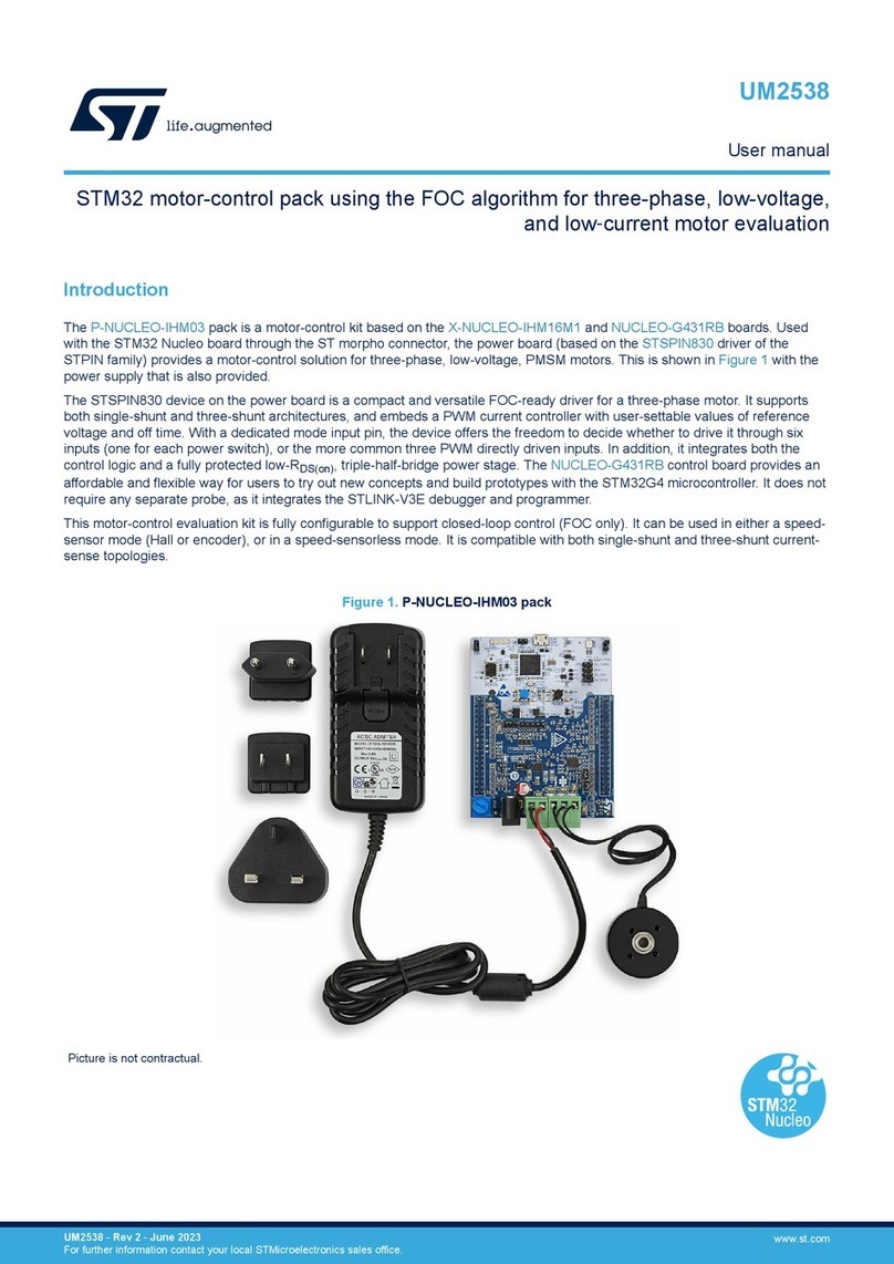
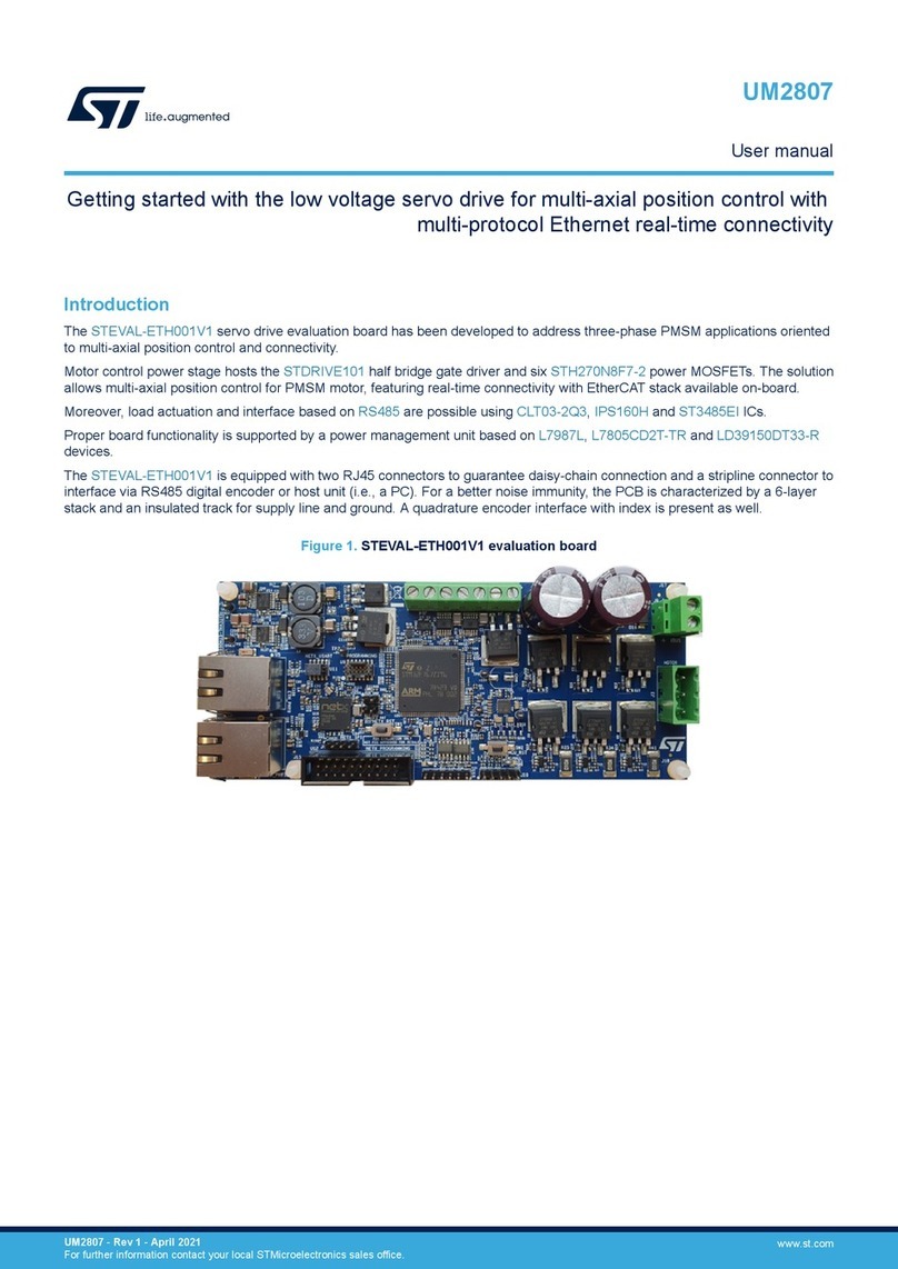
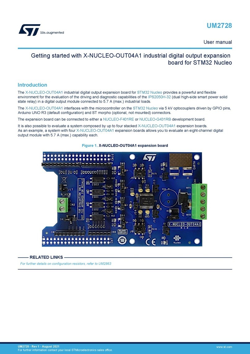
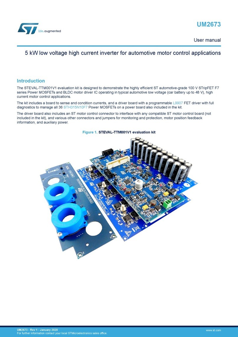
ST STM32U5 User manual

Introduction
The STM32U5 Nucleo-144 board based on the MB1549 reference board (NUCLEO-U575ZI-Q) provides an affordable and
flexible way for users to try out new concepts and build prototypes by choosing from the various combinations of performance
and power consumption features, provided by the STM32U5 microcontroller.
The ST Zio connector, which extends the ARDUINO® Uno V3 connectivity, and the ST morpho headers provide easy expansion
of the functionality of the STM32 Nucleo open development platform with a wide choice of specialized shields.
The STM32U5 Nucleo-144 board does not require any separate probe as it integrates the STLINK-V3E debugger/programmer.
The STM32U5 Nucleo-144 board comes with the STM32 comprehensive free software libraries and examples available with the
STM32CubeU5 MCU Package.
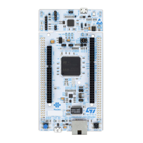
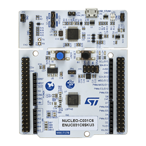
Figure 1. STM32U5 Nucleo-144 board
Picture is not contractual.
STM32U5 Nucleo-144 board (MB1549)
UM2861
User manual
UM2861 - Rev 2 - September 2021
For further information contact your local STMicroelectronics sales office. www.st.com

1Features
•STM32U5 Series microcontroller (Arm® Cortex®-M33 at 160 MHz) in LQFP144 package
• Internal SMPS to generate Vcore logic supply, identified by '-Q' suffixed boards(1)
• USB Type-C® sink device FS
• 3 user LEDs
• RESET and USER push-buttons
• 32.768 kHz crystal oscillator
• Board connectors:
–USB Type-C® connector
–ST Zio connector including ARDUINO® Uno V3
– ST morpho extension pin headers for full access to all STM32 I/Os
• Flexible power-supply options: ST-LINK, USB VBUS, or external sources
• On-board STLINK-V3E debugger/programmer with USB re-enumeration capability: mass storage, Virtual
COM port, and debug port
• Comprehensive free software libraries and examples available with the STM32CubeU5 MCU Package
• Support of a wide choice of Integrated Development Environments (IDEs) including IAR Embedded
Workbench®, MDK-ARM, and STM32CubeIDE
1. SMPS significantly reduces power consumption in Run mode, by generating Vcore logic supply from an internal DC/DC
converter.
Note: Arm is a registered trademark of Arm Limited (or its subsidiaries) in the US and/or elsewhere.
UM2861
Features
UM2861 - Rev 2 page 2/49

2Ordering information
To order the NUCLEO-U575ZI-Q Nucleo-144 board, refer to Table 1. Additional information is available from the
datasheet and reference manual of the target STM32.
Table 1. Ordering information
Order code Board reference Target STM32
NUCLEO-U575ZI-Q MB1549 STM32U575ZIT6Q
2.1 Products and codification
The meaning of the codification is explained in Table 1.
Table 2. Codification explanation
NUCLEO-XXYYZE-Q Description Example: NUCLEO-U575ZI-Q
XX MCU series in STM32 Arm Cortex MCUs STM32U5 Series
YY MCU product line in the series STM32U575/585
Z STM32 package pin count 144 pins
E
STM32 Flash memory size:
• I for 2 Mbytes
• J for 4 Mbytes
2 Mbytes
-Q STM32 has an internal SMPS function SMPS
The order code is mentioned on a sticker placed on the top or bottom side of the board.
UM2861
Ordering information
UM2861 - Rev 2 page 3/49

3Development environment
3.1 System requirements
• Multi‑OS support: Windows® 10, Linux® 64-bit, or macOS®
• USB Type-A or USB Type-C® to Micro-B cable
Note: macOS® is a trademark of Apple Inc. registered in the U.S. and other countries.
Linux® is a registered trademark of Linus Torvalds.
All other trademarks are the property of their respective owners.
3.2 Development toolchains
• IAR Systems® - IAR Embedded Workbench®(1)
• Keil® - MDK-ARM(1)
• STMicroelectronics - STM32CubeIDE
1. On Windows® only.
3.3 Demonstration software
The demonstration software, included in the STM32Cube MCU Package corresponding to the on-board
microcontroller, is preloaded in the STM32 Flash memory for easy demonstration of the device peripherals in
standalone mode. The latest versions of the demonstration source code and associated documentation can be
downloaded from www.st.com.
UM2861
Development environment
UM2861 - Rev 2 page 4/49

4Conventions
Table 3 provides the conventions used for the ON and OFF settings in the present document.
Table 3. ON/OFF convention
Convention Definition
Jumper JPx ON Jumper fitted
Jumper JPx OFF Jumper not fitted
Jumper JPx [1-2] Jumper fitted between Pin 1 and Pin 2
Solder bridge SBx ON SBx connections closed by 0 Ω resistor
Solder bridge SBx OFF SBx connections left open
Resistor Rx ON Resistor soldered
Resistor Rx OFF Resistor not soldered
UM2861
Conventions
UM2861 - Rev 2 page 5/49

5Quick start
The STM32U5 Nucleo-144 board is a low-cost and easy-to-use development kit, to quickly evaluate and start
development with an STM32U5 Series microcontroller in an LFQFP144-pin package. Before installing and using
the product, accept the Evaluation Product License Agreement from the www.st.com/epla webpage. For more
information on the STM32U5 Nucleo-144 board and demonstration software, visit the www.st.com/stm32nucleo
webpage.
5.1 Getting started
Follow the sequence below to configure the STM32U5 Nucleo-144 board and launch the demonstration
application (refer to Figure 4 for component location):
1. Check the jumper position on the board (refer to Default board configuration).
2. For the correct identification of the device interfaces from the host PC and before connecting the board,
install the STLINK-V3E USB driver available on the www.st.com website.
3. Connect the STM32U5 Nucleo-144 board to a PC with a USB cable (USB Type-A or USB Type-C® to
Micro-B) through the USB connector CN1 to power the board.
4. The LD5 5V_PWR green LED and LD4 COM LED light up, and the green LD1 blinks.
5. Press the B1 blue user button.
6. Observe how the blinking of the LEDs LD1, LD2, and LD3 changes, according to clicks on button B1.
7. Download the demonstration software and several software examples that help to use the STM32 Nucleo
features. These are available on the www.st.com website.
8. Develop your application using the available examples.
5.2 Default board configuration
By default, the STM32U5 Nucleo-144 board is configured with VDD_MCU@3V3. It is possible to set the board for
VDD_MCU@1V8. Before switching to 1V8, check that the extension module and external shield connected to the
NUCLEO board are 1.8 V compatible.
The default jumper configuration and voltage setting are shown in Table 4.
Table 4. Default jumper configuration
Jumper Definition Default position Comment
JP1 STLK_NRST OFF STLINK-V3E MCU not under reset mode
JP2 T_NRST ON RST connected between MCU target
and debugger
JP4 VDD [1-2] VDD MCU voltage selection 3V3
JP5 IDD measurement ON MCU VDD current measurement
JP6 5V power selection [1-2] 5V from STLINK-V3E
JP7 UCPD_DBCC1 OFF Refer to Section 6.11.2 UCPD.
JP8 UCPD_DBCC2 OFF Refer to section Section 6.11.2 UCPD.
UM2861
Quick start
UM2861 - Rev 2 page 6/49

Figure 2. Default board configuration
UM2861
Default board configuration
UM2861 - Rev 2 page 7/49

Table 5 explains the other jumper settings and configurations.
Table 5. Jumper configuration
Jumper Definition Setting(1) Comment
JP1 STLK_RST
ON Use to reset the STLINK-V3E MCU
when an external debug probe is used.
OFF Normal mode: use the STLINK-V3E
debug probe
JP2 T_NRST
ON STLINK-V3E able to reset target MCU
OFF
STLINK-V3E not able to reset Target
MCU configuration to use when an
external debug probe is used.
JP4 VDD voltage selection
[1-2] VDD voltage selection is 3V3
[2-3] VDD voltage selection is 1V8
OFF No internal VDD power supply
(External 3V3 or 1V8 needed)
JP5 IDD measurement
ON MCU is powered by the on‑board
power supplies.
OFF
Use an ammeter to measure the MCU
power consumption, or connect an
external source 3V3 or 1V8 on pin
2 to supply the MCU (STLINK-PWR
tools with STM32CubeMonitor-Power or
ULPBench probe as exemple)
JP6 5V Power selection
[1-2] 5V source from STLINK-V3E
[3-4] 5V source from ARDUINO® VIN 7-12V
[5-6] 5V source from 5V_EXT
[7-8] 5V source from USB Type-C®
[9-10]
5V source from USB_CHGR
(from CN1 STLINK-V3E USB connector
without overcurrent protection)
OFF NO 5V power source, configuration
when external 3V3 is used.
JP7 UCPD_DBCC1
OFF UCPD_DBCC1 NOT connected to
GND
ON UCPD_DBCC1 connected to GND (For
debug purpose)
JP8 UCPD_DBCC2
OFF UCPD_DBCC2 NOT connected to
GND
ON UCPD_DBCC2 connected to GND (For
debug purpose)
1. The default configuration is in bold.
UM2861
Default board configuration
UM2861 - Rev 2 page 8/49

6Hardware layout and configuration
The STM32U5 Nucleo-144 board is designed around an STM32U5 microcontroller in an LFQFP 144-pin package.
Figure 3 shows the connections between the STM32 and its peripherals (STLINK-V3E, push‑buttons, LEDs, USB
ST Zio connectors, and ST morpho headers). Figure 4 and Figure 5 show the location of these features on the
STM32U5 Nucleo-144 board.
The mechanical dimensions of the board are shown in Figure 6.
Figure 3. Hardware block diagram
STM32U575ZI-Q
OSC_32
SWD
32KHz
Crystal
VCP
UART
GPIOs
GPIO
LED
GPIO
Embedded
STLINK-V3E
STDC14/MIPI10
SWD VCP
UART
USB MicroB
connector
B1
User
B2
RST
ARDUINO
MORPHO
GPIO
ARDUINO
MORPHO
5V
PWR SEL
5V
LED
RES COM
T_NRST
STLK
NRST
LEDLED
IDD1V8 / 3V3
USB Type C
connector
GND
GND
GNDGND
SWDUART
UM2861
Hardware layout and configuration
UM2861 - Rev 2 page 9/49

6.1 STM32U5 Nucleo-144 board layout
Figure 4. STM32U5 Nucleo-144 board top layout
UM2861
STM32U5 Nucleo-144 board layout
UM2861 - Rev 2 page 10/49

Figure 5. STM32U5 Nucleo-144 board bottom layout
UM2861
STM32U5 Nucleo-144 board layout
UM2861 - Rev 2 page 11/49

6.2 Mechanical drawing
Figure 6. STM32U5 Nucleo-144 board mechanical drawing (in millimeter)
UM2861
Mechanical drawing
UM2861 - Rev 2 page 12/49

6.3 Embedded STLINK-V3E
There are two different ways to program and debug the onboard STM32 MCU:
• Using the STLINK-V3E programming and debugging tool on the STM32U5 Nucleo-144
• Using an external debug tool connected to the CN5 STDC14/MIPI-10 connector
The STLINK-V3E makes the NUCLEO-U575ZI-Q Nucleo-144 board Arm® Mbed Enabled™.
The embedded STLINK-V3E supports only SWD and VCP for STM32 devices. For information about debugging
and programming features of STLINK-V3, refer to the user manual STLINK-V3SET debugger/programmer for
STM8 and STM32 (UM2448) which describes in detail all the STLINK-V3 features.
STLINK-V3E description:
• 5V power supplied by CN1 USB connector
• USB 2.0 high-speed compatible interface
• JTAG and SWD protocols compatible with 1.7 to 3.6 V application voltage and 5 V tolerant input I/Os
• Serial wire viewer (SWV) output
• STDC14 MIPI-10 compatible connector (CN5)
• COM status LED blinking during communication with the PC (LD4)
• 5 V/300 mA output power supply capability with current limitation (U2)
• OC fault red LED alerting on USB overcurrent request (LD6)
• 5V_PWR 5 V power green LED (LD5)
Table 6 describes the CN1 USB Micro-B connector pinout.
Table 6. CN1 USB Micro-B connector pinout
Pin Pin name Signal name STLINK-V3E STM32 pin Function
1 VBUS 5V_USB_CHGR - VBUS Power
2 DM USB_DEV_HS_CN_N PB14 DM
3 DP USB_DEV_HS_CN_P PB15 DP
4 ID - - ID
5 GND GND GND GND
UM2861
Embedded STLINK-V3E
UM2861 - Rev 2 page 13/49

6.3.1 Drivers
Before connecting the STM32U5 Nucleo-144 board to a Windows 7®, Windows 8®, or Windows 10® PC via USB,
a driver for the STLINK-V3E (stsw-link009) must be installed (not required for Windows 10®). It is available on the
www.st.com website.
In case the STM32U5 Nucleo-144 board is connected to the PC before the driver is installed, a peripheral may be
declared as “Unknown” in the PC device manager. In this case, the user must install or update the driver files from
the device manager as shown in Figure 7.
Note: Prefer using the USB Composite Device handle for a full recovery.
Figure 7. USB composite device
Note: 37xx:
• 374E for STLINK-V3E without bridge functions
• 374F for STLINK-V3E with bridge functions
6.3.2 STLINK-V3E firmware upgrade
The STLINK-V3E embeds a firmware upgrade mechanism through the USB port. As the firmware may evolve
during the lifetime of the STLINK-V3E product, to add new functionalities, to fix bugs, and to support new
microcontroller families, it is recommended to visit the www.st.com website before starting to use the STM32U5
Nucleo-144 board and periodically, to stay up-to-date with the latest firmware version.
UM2861
Embedded STLINK-V3E
UM2861 - Rev 2 page 14/49

6.3.3 Using an external debug tool to program and debug the on-board STM32
There are two basic ways to support an external debug tool:
1. Keep the embedded STLINK-V3E running. Power on the STLINK-V3E at first until the COM LED turns red.
Then connect the external debug tool through the CN5 STDC14/MIPI-10 debug connector
2. Set the embedded STLINK-V3E in a high-impedance state. When the JP1 STLK_RST jumper is ON, the
embedded STLINK-V3E is in RESET state and all GPIOs are in high impedance. Remove JP2 to avoid
driving MCU T_NRST. Then, connect the external debug tool to the CN5 STDC14/MIPI‑10 debug connector.
Figure 8. Connecting an external debug tool to program the on-board STM32U5
UM2861
Embedded STLINK-V3E
UM2861 - Rev 2 page 15/49

Figure 9 shows the CN5 STDC14/MIPI-10 connector.
Figure 9. CN5 STDC14/MIPI-10 debug connector
Table 7 describes the STDC14/MIPI-10 connector pinout.
Table 7. CN5 STDC14/MIPI-10 debug connector pinout
MIPI-10 pin STDC14 pin CN5 Function
- 1 NC Reserved
- 2 NC Reserved
1 3 VDD Target VDD
2 4 T_SWDIO Target SWDIO using SWD protocol or target JTMS (T_JTMS) using
JTAG protocol
3 5 GND Ground
4 6 T_SWCLK Target SWCLK using SWD protocol or target JTCK (T_JTCK) using
JTAG protocol
5 7 GND Ground
6 8 T_SWO Target SWO using SWD protocol or target JTDO (T_JTDO) using JTAG
protocol (SB44 ON)
7 9 NC -
8 10 T_JTDI Not used by SWD protocol, target JTDI (T_JTDI) using JTAG protocol,
only for external tools (SB39 OFF)
9 11 GNDDetect GND detect for plug indicator
10 12 T_NRST Target NRST using SWD protocol or target JTMS (T_JTMS) using
JTAG protocol
- 13 T_VCP_RX Target RX used for VCP (with UART supporting bootloader)
- 14 T_VCP_TX Target TX used for VCP (with UART supporting bootloader)
Two SN74LVC2T45DCUT level shifters are used on VCP and SWD interface to offer a debug capability with 1V8
powered MCU. One level shifter is used for a signal from the MCU target (1V8) to STLINK-V3E (3V3).
• U1 used for T_VCP_TX signal
• U9 used for T_SWDIO and T_SWO signal
UM2861
Embedded STLINK-V3E
UM2861 - Rev 2 page 16/49

6.4 Power supply and power selection
6.4.1 External power supply input
The Nucleo board is designed to be powered by several DC power supplies. It is possible to configure the Nucleo
board to use any of the following sources for the power supply:
• 5V_STLK from CN1 STLINK-V3E USB connector
• VIN (7 to 12 V) from CN8 ARDUINO®-included Zio connector or CN11 ST morpho connector
• 5V_EXT from CN11 ST morpho connector
• 5V_USB_C from CN15 USB Type-C® connector
• 5V_CHGR from CN1 STLINK-V3E USB connector
• 3V3 from CN8 ARDUINO®-included Zio connector or CN11 ST morpho connector
If VIN, 5V_EXT, or 3V3 is used to power a Nucleo-144 board, this power source must comply with the standard
EN‑60950‑1: 2006+A11/2009 and must be safety extra‑low voltage (SELV) with limited power capability.
The power supply capabilities are summarized in Table 8.
Table 8. Power sources capability
Input Power name Connector pins Voltage range Max.
current Limitation
5V_STLK CN1 pin 1
JP6 [1-2] 4.75 to 5.25 V 500 mA
Maximum current depending on the presence or
absence of USB enumeration:
• 100 mA without enumeration
• 500 mA with enumeration OK
VIN / 5V_VIN
CN8 pin 15
CN11 pin 24
JP6 [3-4]
7 to 12 V 800 mA
From 7 to 12 V only and input current capability is
linked to input voltage:
• 800 mA input current when VIN = 7 V
• 450 mA input current when 7 V < VIN < 9 V
• 250 mA input current when 9 V < VIN < 12 V
5V_EXT CN11 pin 6
JP6 [5-6] 4.75 to 5.25 V 500 mA Maximum current depending on the power source
5V_USB_C CN15
JP6 [7-8] 4.75 to 5.25 V 1 A Maximum current depending on the USB host used
to power the Nucleo
5V_CHGR CN1 pin 1
JP6 [9-10] 4.75 to 5.25 V 500 mA Maximum current depending on the USB wall
charger used to power the Nucleo
3V3
CN8 pin 7
CN11 pin 16
JP5 pin 2
3.0 to 3.6 V -
Maximum current depending on the 3V3 source.
Used when the ST-LINK part of PCB is not used or
removed. SB1 must be OFF to protect LDO U6.
5V_STLK is a DC power with the limitation from the STLINK-V3E USB connector (USB Type Micro-B connector
of STLINK-V3E). In this case, the JP6 jumper must be on pin [1-2] to select the 5V_STLK power source.
This is the default setting. If the USB enumeration succeeds, the 5V_STLK power is enabled, by asserting the
T_PWR_EN signal from U6 STLINK-V3E MCU. This pin is connected to the U2 power switch, which powers
the board. This power switch also features a 500 mA current limitation, to protect the PC in case of an onboard
short-circuit.
The STM32U5 Nucleo-144 board with its shield can be powered from the CN1 STLINK-V3E USB connector, but
only the STLINK-V3E circuit has the power before USB enumeration because the host PC only provides 100mA
to the board at that time. During the USB enumeration, the Nucleo board asks for a 500mA power to the host PC.
• If the host can provide the required power, the enumeration finishes by a SetConfiguration command
and then, the U2 power switch is switched ON, the Green LED LD5 is turned ON, thus the Nucleo board with
its shield can consume 500mA current, but no more.
UM2861
Power supply and power selection
UM2861 - Rev 2 page 17/49

• If the host is not able to provide the requested current, the enumeration fails. Therefore, the U2 power switch
remains OFF and the MCU part including the extension board is not powered. As a consequence, the LD5
green LED remains OFF. In this case, it is mandatory to use an external power supply.
5V_STLK configuration: The JP6 jumper is set on [1-2] as shown in Figure 10.
Figure 10. JP6 [1-2]: 5V_STLK power source
UM2861
Power supply and power selection
UM2861 - Rev 2 page 18/49

VIN (5V_VIN) is the 7 to 12 V DC power from the CN8 ARDUINO®‑included Zio connector pin 15 named VIN on
the connector silkscreen, or from the CN11 ST morpho connector pin 24. In this case, the JP6 jumper must be on
pin [3-4] to select the 5V_VIN power source. In that case, the DC power comes from the power supply through the
ARDUINO® Uno V3 battery shield (compatible with Adafruit PowerBoost 500 shield).
5V_VIN configuration: The JP6 jumper must be set on [3-4] as shown in Figure 11.
Figure 11. JP6 [3-4]: 5V_VIN power source
UM2861
Power supply and power selection
UM2861 - Rev 2 page 19/49

5V_EXT is the DC power coming from an external 5 V DC power from the CN11 ST morpho connector pin 6. In
this case, the JP6 jumper must be set on [5-6] to select the 5V_EXT power source.
5V_EXT configuration: The JP6 jumper must be set on [5-6] as shown in Figure 12.
Figure 12. JP6 [5-6]: 5V_EXT power source
UM2861
Power supply and power selection
UM2861 - Rev 2 page 20/49
Other manuals for STM32U5
2
Table of contents
Other ST Computer Hardware manuals

ST
ST X-NUCLEO-IHM02A1 User manual

ST
ST X-NUCLEO-DRP1M1 User manual

ST
ST X-CUBE-SBSFU User manual

ST
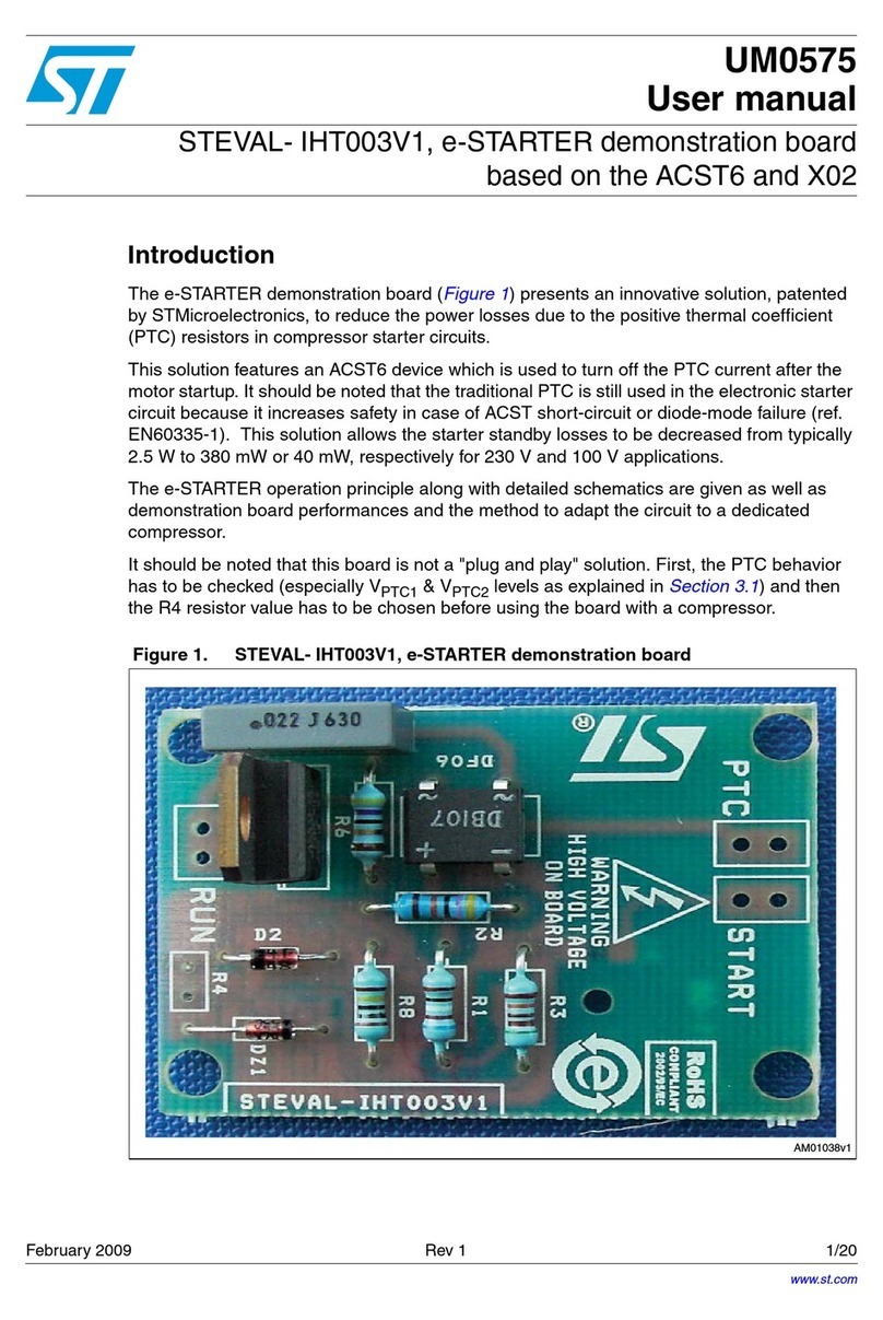
ST UM0575 User manual

ST
ST X-NUCLEO-OUT19A1 User manual

ST
ST ControlBD-7FMC2 User manual

ST
ST STM32U5G9J-DK2 User manual

ST
ST X-NUCLEO-S2915A1 User manual

ST
ST X-NUCLEO-OUT02A1 User manual

ST
ST STEVAL-DPSG474 User manual

ST
ST STEVAL-IDZ3V1 Series User manual

ST
ST X-NUCLEO-OUT01A2 User manual

ST
ST STM32F038 6 Series User manual

ST
ST STM32U5 User manual

ST
ST STM32U575 Series Installation and operating instructions

ST
ST M41ST85W User manual

ST
ST X-NUCLEO-IHM14A1 User manual

ST
ST X-CUBE-OUT3 User manual

ST
ST STM32F3 Series Owner's manual

ST
ST AEK-LCD-DT028V1 User manual