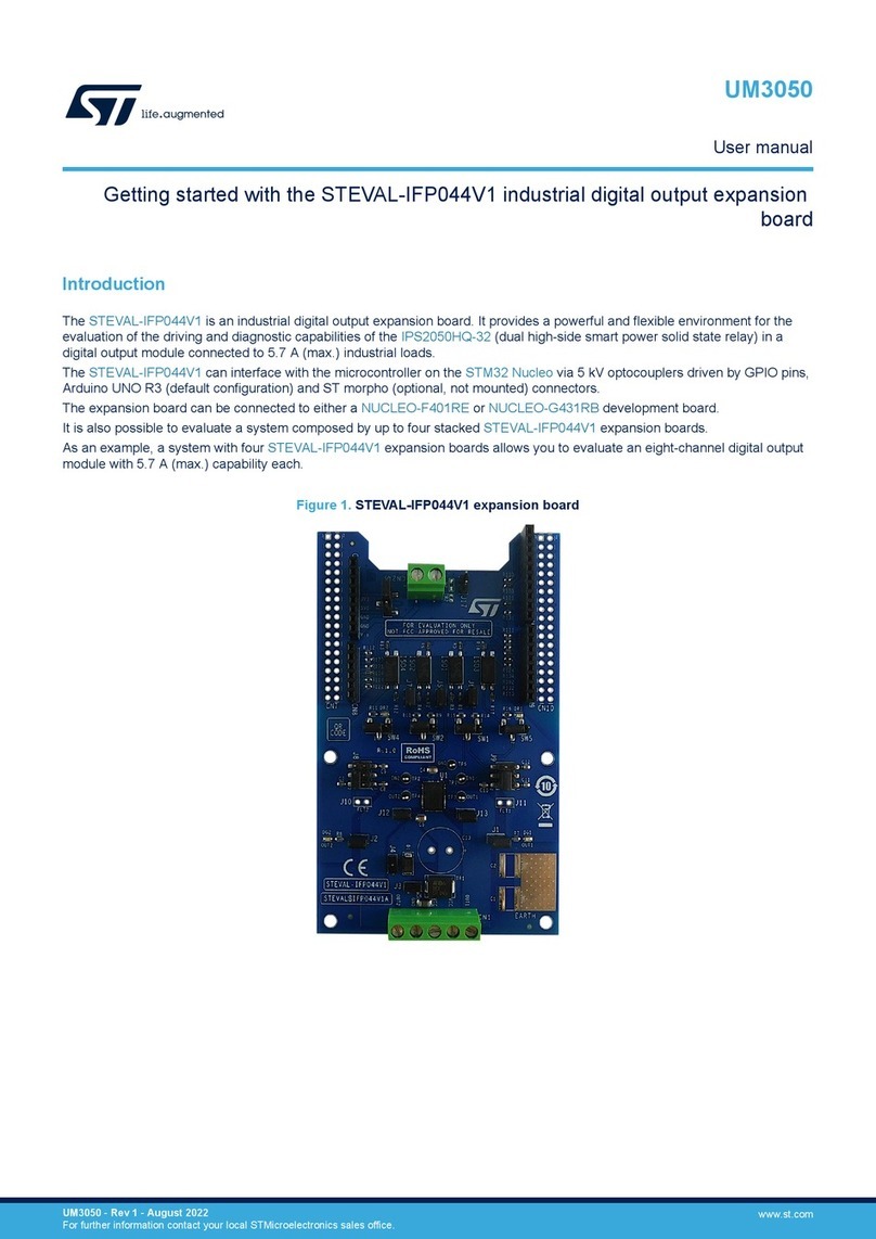
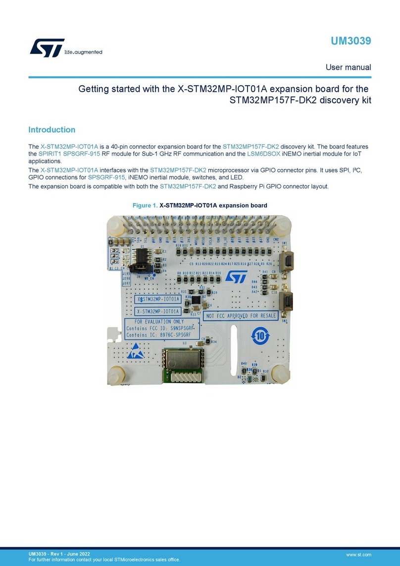
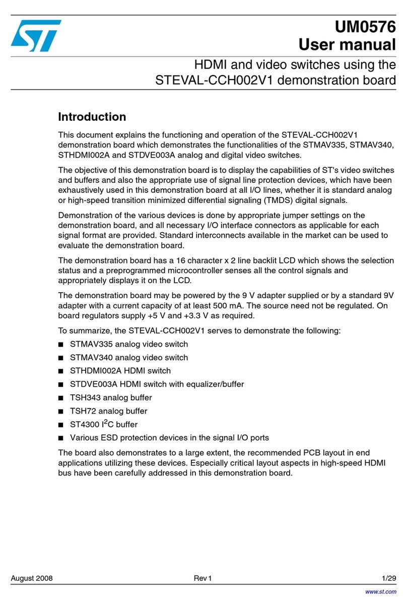
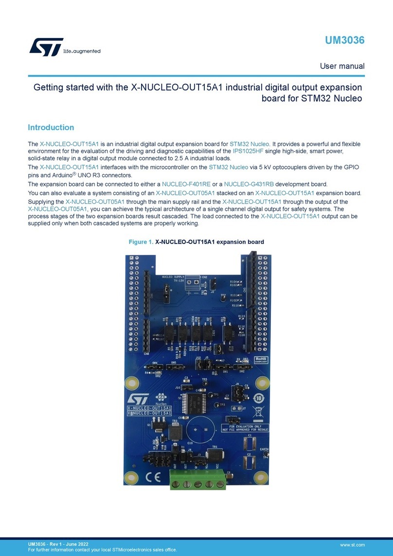
ST STM32WL Series User manual

Introduction
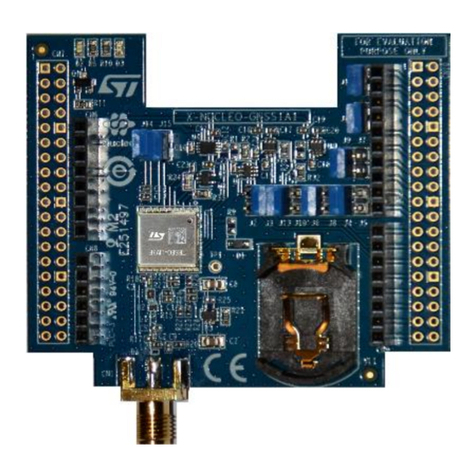
The B-WL5M-SUBG1 STM32WL connectivity expansion board provides an affordable and flexible way for users to try out new
concepts and build prototypes with the STM32WL series STM32WL5MOC microcontroller module.
The B-WL5M-SUBG1 product requires a separate probe for programming and debugging. The STLINK-V3SET debugger can
be connected through a MIPI10/STDC14 cable.
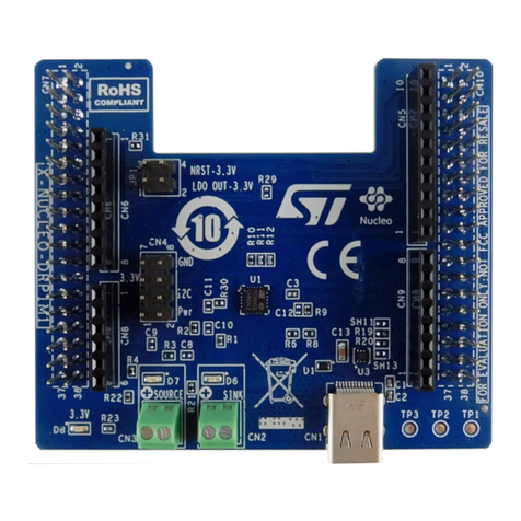
The B-WL5M-SUBG1 STM32WL connectivity expansion board is provided with a USB Type-C® connector on an add-on
STMod+ adapter board.
The B-WL5M-SUBG1 product is provided with the STM32WL comprehensive software HAL library and various packaged
software examples available with the STM32CubeWL MCU Package.
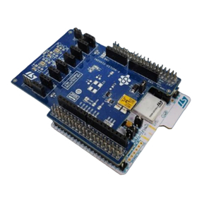
Figure 1. B-WL5M-SUBG1 product
Picture is not contractual.
STM32WL5MOC connectivity expansion board
UM3127
User manual
UM3127 - Rev 1 - January 2024
For further information contact your local STMicroelectronics sales office. www.st.com

1 Features
• STM32WL connectivity expansion board embedding an STM32WL5MOC module including:
– Ultra‑low‑power STM32WL55JC microcontroller multiprotocol LPWAN dual‑core based on
Arm® Cortex®‑M4/M0+, featuring 256 Kbytes of flash memory and 64 Kbytes of SRAM in a
UFBGA73 package
– RF transceiver (150 MHz to 960 MHz frequency range) supporting LoRa®, (G)FSK, (G)MSK, and
BPSK modulations
• 4‑Mbit CMOS serial flash memory and 256‑Kbit serial I2C bus EEPROM
• MEMS sensors from STMicroelectronics:
– Integrated high-accuracy temperature sensor
– High-accuracy, ultra-low-power, 3-axis digital output magnetometer
– 3D accelerometer and 3D gyroscope
– Ultracompact piezoresistive absolute pressure sensor
• Three user LEDs
• User and reset push-buttons
• Board connectors:
–MIPI® debug
– STMod+
– Stubby antenna
– USB Type-C® for power only on add‑on STMod+ adapter board
• Flexible power supply options: external sources, or USB VBUS from the add‑on board
• Comprehensive free software libraries and examples available with the STM32CubeWL MCU Package
• Support of a wide choice of Integrated Development Environments (IDEs) including IAR Embedded
Workbench®, MDK-ARM, and STM32CubeIDE
Note: Arm is a registered trademark of Arm Limited (or its subsidiaries) in the US and/or elsewhere.
UM3127
Features
UM3127 - Rev 1 page 2/47

2 Ordering information
To order the B-WL5M-SUBG1 STM32WL connectivity expansion board, refer to Table 1. Additional information is
available from the datasheet and reference manual of the target microcontroller.
Table 1. List of available products
Order code Board reference Target STM32
B-WL5M-SUBG1 • MB1779(1)
• MB1880(2) STM32WL5MOCH6TR
1. Expansion board
2. STMod+ adapter board
2.1 Codification
The meaning of the codification is explained in Table 2.
Table 2. Codification explanation
B-XXYY-ZZZZT Description Example: B-WL5M-SUBG1
B Expansion board Connectivity expansion board
XX MCU series in STM32 32-bit Arm Cortex MCUs STM32WL series
YY MCU product line in the series STM32WL5M line
ZZZZ Wireless network Sub‑gigahertz wireless network based on LoRa®, (G)FSK,
(G)MSK, and BPSK modulations
T Sequential number First SUBG connectivity expansion board
UM3127
Ordering information
UM3127 - Rev 1 page 3/47

3 Development environment
The B-WL5M-SUBG1 STM32WL connectivity expansion board runs with the STM32WL5MOC module including
the STM32WL5MOCH6 32-bit microcontroller based on the Arm® Cortex®‑M4/M0+ processor.
3.1 System requirements
• Multi‑OS support: Windows® 10, Linux® 64-bit, or macOS®
• USB Type-A or USB Type-C® to USB Type-C® cable
Note: macOS® is a trademark of Apple Inc., registered in the U.S. and other countries and regions.
Linux® is a registered trademark of Linus Torvalds.
Windows is a trademark of the Microsoft group of companies.
3.2 Development toolchains
•IAR Systems® - IAR Embedded Workbench®(1)
•Keil® - MDK-ARM(1)
• STMicroelectronics - STM32CubeIDE
1. On Windows® only.
UM3127
Development environment
UM3127 - Rev 1 page 4/47

4 Conventions
Table 3 provides the conventions used for the ON and OFF settings in the present document.
Table 3. ON/OFF convention
Convention Definition
Jumper JPx ON Jumper fitted
Jumper JPx OFF Jumper not fitted
Jumper JPx [1-2] Jumper fitted between Pin 1 and Pin 2
Solder bridge SBx ON SBx connections closed by 0 Ω resistor
Solder bridge SBx OFF SBx connections left open
Resistor Rx ON Resistor soldered
Resistor Rx OFF Resistor not soldered
Capacitor Cx ON Capacitor soldered
Capacitor Cx OFF Capacitor not soldered
UM3127
Conventions
UM3127 - Rev 1 page 5/47

5 Quick start
The B-WL5M-SUBG1 STM32WL connectivity expansion board product is an easy‑to‑use and low‑cost
development kit used to evaluate and start development quickly with an STM32WL5MOC module. Before
installing and using the product, accept the evaluation product license agreement from the www.st.com/epla web
page. For more information on the B-WL5M-SUBG1 STM32WL connectivity expansion board product and
demonstration software, visit the www.st.com/stm32nucleo web page.
5.1 Getting started
Follow the sequence below to configure the product and launch the demonstration application (refer to Figure 3
for component location):
1. Check jumper positions on board, JP2 (IDD) ON, JP1 (internal) OFF. The default jumper position on the board
is explained in Table 4.
2. Supply the B-WL5M-SUBG1 STM32WL connectivity expansion board (MB1779). You can, for example,
connect a supply cable at CN4 to supply the board with 5 V (5EV).
3. Connect the B-WL5M-SUBG1 STM32WL connectivity expansion board (MB1779) to an external STLINK-
V3SET debugger through the CN3 connector of the MB1779 board. Connect the external STLINK-V3SET
debugger to a PC with a standard USB cable. Then the LED4 (5V_PWR) green LED lights up, and the LED3
red LED flashes quickly.
4. On the PC, connect a UART terminal to the board using the following settings:
– UART terminal: new line received = auto; new line transmit = LF (line feed)
– Serial port setting: Select COM port number, 9600 baud rate, 8-bit data, parity none, one stop bit, and no
flow control
5. Press on the SW2 reset button of the B-WL5M-SUBG1 STM32WL connectivity expansion board (MB1779).
– The MB1779 board remains silent until it gets a command from the connected PC to start sending a
beacon on one of the beacon frequencies.
– The frequency is selected depending on the region.
– After the version check, the first three commands to send to the PC must set region, subregion, and
start the beacon (AT+REGION=x and AT_BEACON_ON). The first two commands select the format of
the transmission beacon. The third command starts sending the beacon.
– For a list of available regions run AT_LIST_REGIONS.
6. Then a concentrator (for example a NUCLEO-WL55JC1 board) starts flashing a green LED on each time slot
of the network.
7. To get the demonstration fully up and running, up to 14 B-WL5M-SUBG1 STM32WL connectivity expansion
board (MB1779) demonstration sensors can be flashed and placed against a Nucleo demonstration
concentrator.
8. This demonstration application software is available on the www.st.com website.
Table 4. Jumper default configuration
Jumper Definition Position(1) Comment
JP2 IDD ON For STM32WL5MOC current
measurements (RF part)
1. The default jumper state is shown in bold.
UM3127
Quick start
UM3127 - Rev 1 page 6/47

6 Hardware layout and configuration
6.1 CEB MB1779 board
The CEB (connectivity expansion board) MB1779 board is designed around the STM32WL5MOC module, which
includes an STM32 microcontroller in a 73‑pin UFBGA package. Figure 2 shows the connections between the
STM32WL5MOC module and its peripherals, push-buttons, LEDs, USB, and sensors. Figure 3 and Figure 4 show
the location of these features on the CEB MB1779 board. The mechanical dimensions of the board are shown in
Figure 5.
Figure 2. MB1779 hardware block diagram
DT59126V1
STM32WL55
Reset
button
GPIO
DEBUG
IDD
32 MHz
TCXO
Blue user LED (LD1)
Green 5V_PWR
LED (LD4)
User
button
Green User LED (LD2)
Red User LED (LD3)
RF switch/
control
and
RF
matching
SMA
connector
(CN2)
VCP SWD
32 kHz
Crystal
STM32WL5MOC module
ST-SAFE
STMod+
connector
(CN1)
E5V
Temperature
sensor (U14)
Barometer
(U4)
Accelerometer-
gyroscope
(U2)
Magnetometer
(U7)
I2C
SPI
Serial flash
memory
I2C bus
EEPROM
(CN4)
(U10)
(U8)
(U14)
(U4)
(U2)
(U7)
(SW2) (SW1)(CN3)
(U3)
(JP2)
6.1.1 MB1779 PCB layout
Figure 3. MB1779 top layout
Product
sticker
Barometer (U4)
E5V supply
connector
(CN4)
STM32WL5M module
(U3)
3V3 regulator (U6)
SMA antenna
connector
(CN2)
3D accelerometer and 3D gyroscope (U2)
E3V3 supply
connector
(CN5)
STDC14 debug
Connector
(CN3)
USER button
(SW1)
I2C EEPROM
(U8)
Magnetometer
(U7)
Temperature sensor
(U14) CMOS
serial flash memory
(U10) User LEDs
(LD1, LD2,
and LD3)
RESET button
(SW2)
IDD jumper for
current measurement
(JP2 ON)
STMod+
connector
(CN1)
DC switches
(U1 and U5)
UM3127
Hardware layout and configuration
UM3127 - Rev 1 page 7/47

Figure 4. MB1779 bottom layout
DT59129V1
EMS sticker
(reserved for EMS)
Board sticker
SMA antenna
connector
(CN2)
E5V supply
connector
(U15)
UID64 sticker
STMod+
connector
(CN1)
• The UID64 sticker:
A 64-bit unique device identification (UID64) is stored in the flash memory and can be accessed by the
CPUs, at 0x1FFF7580 base address.
The UID64 sticker displays the UID information (16 digits as 64‑bit codification, displayed in little‑endian
bytes) which is unique for each STM32WL5MOC module.
• The EMS sticker:
This sticker is an internal follow‑up sticker for the EMS subcontractor. Do not take it into account.
6.1.2 MB1779 mechanical drawing
Figure 5. MB1779 mechanical drawing
UM3127
Hardware layout and configuration
UM3127 - Rev 1 page 8/47

6.2 MB1880 STMod+ adapter board
The MB1880 STMod+ adapter board is a very simple board that allows the MB1779 connectivity expansion board
to become a host with the add-on STMod+ connectors (female).
Figure 6 shows the basic hardware block diagram. Figure 7 and Figure 8 show the location of the main
components of the MB1880 board. The mechanical dimensions of the board are shown in Figure 9.
Figure 6. MB1880 basic hardware block diagram
DT59131V1
JP1
STMod+
connector
(CN2)
STMod+
connector
(CN3)
USB C
(CN1)
JP2
6.2.1 MB1880 PCB layout
Figure 7. MB1880 top layout
DT59132V1
STMod+
connector
(CN2)
Jumper
(JP1)
5V test point
(TP2)
GND test point
(TP1)
Jumper
(JP2)
STMod+
connector
(CN3)
ESDA7P60-1U1M
ESD protection
(U1)
USB Type-C®
connector
(CN1)
UM3127
Hardware layout and configuration
UM3127 - Rev 1 page 9/47

Figure 8. MB1880 bottom layout
DT59133V1
STMod+
connector
(CN3)
Board sticker
EMS sticker
(reserved for EMS)
STMod+
connector
(CN2)
Two stickers (the board sticker and an EMS sticker) are present on the bottom side of the MB1880 board:
1. The board sticker is composed of three parts:
a. Line 1: board reference using the format MBxxxx-Variant-yzz with xxxx as the board reference,
Variant as the board variant, coded on 26 digits maximum, y as the PCB revision, and zz as the
assembly revision, such as 01 or 02.
b. Line 2: board serial number coded on 10 digits syywwxxxxx with s as the subcontractor ID, yy the year of
assembly, ww the week of assembly, and xxxxx the board index number starting from 00001 for each
production batch.
c. QR code: (25x25; 47 characters maximum) encoding lines one and two information. The QR code is
placed on the right of the two lines.
2. The EMS sticker:
This sticker is an internal follow-up sticker for the EMS subcontractor. Disregard it.
6.2.2 MB1880 mechanical drawing
Figure 9. MB1880 mechanical drawing (in millimeters)
UM3127
Hardware layout and configuration
UM3127 - Rev 1 page 10/47

6.3 Power supply
The following sources can provide the power supply
• Connected to MB1779
– An external E5V 5 V power supply connected to CN4 (preferred solution)
– An external E3V3 3.3 V power supply connected to CN5 (not fitted)
• Connected through the MB1880 STMod+ adapter board
– 5 V via the USB Type-C® connector
– 5 V supplied through a host
Figure 10. CEB MB1779 board power tree
DT59136V1
Sensors:
Temperature (U14)
Digital output barometer (U4)
3D accelerometer and
3D gyroscope (U2)
Digital output magnetometer (U7)
STM32WL5MOC module (U3)
E5V connector
(CN4)
3V3 LDO
U6
E5V
5 V
(VDD_RF)
(VDD_SYS)
(VBAT)
TCXO
RF front-end
(PB0_VDD_TCXO)
VDD_APP
(VREF+)
SB14 ON
3V3
SB38 ON
5 V
VDD
ST-SAFE
DC
switches
(U1, U5)
SB8 ON
Memories:
CMOS serial flash memory (U10)
I2C bus EEPROM (U8)
3V3
3V3_MEMs
SB15 ON
JP2 ON
3V3
E3V3 connector
(CN5)
SB35 OFF
5 V
5 V
STDC14
debug connector
(CN3)
STMod+
connector
(CN1)
VCC
PB8
In case an external voltage supply on E5V/E3V3 is used to power the connectivity expansion board MB1779, this
E5V/E3V3 power source must comply with the EN‑62368-1: 2014+A11:2017 standard and must be safety extra
low voltage(SELV) with limited power capability.
UM3127
Hardware layout and configuration
UM3127 - Rev 1 page 11/47

6.3.1 Power supply input E5V connector (default setting)
The CEB MB1779 board can be powered from the E5V connector (CN4) by either:
• Plugging an external 5 V voltage supply (from 3.6 up to 5.5 V)
• Plugging a 3.7 V battery pack
Refer to Table 5. This is the default setting.
Table 5. External power source E5V (5 V)
Input power name Connector pins Voltage range Maximum current
E5V MB1779 - CN4 pin 1 3.6 to 5.5 V 500 mA
Make sure you supply the board when using CN4. CN4 pin 1 is the E5V supply and pin 2 is the GND, as shown in
Figure 11.
Figure 11. E5V and GND pins on CN4
DT59138V1
GND
E5V
UM3127
Hardware layout and configuration
UM3127 - Rev 1 page 12/47

6.3.2 Power via the STMod+ adapter board (MB1880) supplied through a USB Type-C® connector
The CEB MB1779 board can be powered by 5V coming from the USB Type-C® connector of the STMod+ adapter
board (MB1880). This USB Type-C® connector can be connected to:
• A PC through a USB cable
• A USB charger
This is displayed in Table 6 and Figure 12.
Figure 12. Power supply input from 5V via the STMod+ adapter board (MB1880) connected to a PC
through a USB connector
DT59139V1
PC / USB charger
Table 6. External power source 5V (5 V)
Input power name Connector pins Voltage range Maximum current
5V MB1880 - CN1 5 V 500 mA
6.3.3 Power via STMod+ adapter board (MB1880) supplied through a host
The CEB MB1779 board can be powered by 5V coming from the second STMod+ connector of the STMod+
adapter board (MB1880). This STMod+ connector can be connected to a host.
This is displayed in Figure 13.
Figure 13. Power supply input from 5V via STMod+ adapter board (MB1880) connected to a host
DT59140V1
Host
UM3127
Hardware layout and configuration
UM3127 - Rev 1 page 13/47

6.3.4 Power supply input E3V3 connector
The CEB MB1779 board can be powered by the E3V3 connector (CN5) by plugging an external 3.3 V voltage
supply (up to 3.6 V).
Refer to Table 7.
Table 7. External power source E3V3 (3.3 V)
Input power name Connector pins Voltage range Maximum current
E3V3 MB1779 - CN5 pin 1 Up to 3.6 V 500 mA
Make sure to supply the board when using CN5.
A 2‑pin header must be soldered at CN5.
CN5 pin 1 is the E3V3 supply and pin 2 is the GND, as shown in Figure 14.
Figure 14. E3V3 and GND pins on CN5
DT59141V1
GND
3V3
UM3127
Hardware layout and configuration
UM3127 - Rev 1 page 14/47

6.4 Board functions
6.4.1 LEDs
User LED (LD1)
This blue LED is a user LED connected to STM32WL5MOC module I/O PB15. To light the LD1 LED, a HIGH logic
state must be written in the corresponding GPIO PB15.
User LED (LD2)
This green LED is a user LED connected to STM32WL5MOC module I/O PB9. To light the LD2 LED, a HIGH
logic state must be written in the corresponding GPIO PB9.
User LED (LD3)
This red LED is a user LED connected to STM32WL5MOC module I/O PB11. To light the LD3 LED, a HIGH logic
state must be written in the corresponding GPIO PB11.
5V_PWR LED (LD4)
This green LED indicates that the CEB MB1779 board is powered, and 5 V power is available at the input of the
3V3 regulator (U6) to provide the 3.3 V necessary to supply the STM32WL5MOC module.
6.4.2 Push-buttons
SW1 user button
This user button is connected to the STM32WL5MOC module I/O PA0.
SW2 reset button
This push-button is connected to NRST and is used to reset the STM32WL5MOC module.
6.4.3 RF overview
The CEB MB1779 board embeds an STM32WL5MOC module and DC switches to address with the same board
the three reception, High-power transmission, and Low-power transmission modes. The choice between the two
transmission modes can be done dynamically, thanks to two DC switches controlled by SW_RF (GPIO from the
STM32WL series MCU):
• The transmission high-output power amplifier (PA HP) is supplied from the PA regulator (REG PA) up to
3.1 V. For this, the REG PA must be supplied directly from VDDSMPS.
• The transmission default low-output power amplifier (PA LP) can be supplied from the PA regulator (REG
PA) up to 1.35 V. For this, the REG PA must be supplied from the regulated VFBSMPS supply at 1.55 V.
UM3127
Hardware layout and configuration
UM3127 - Rev 1 page 15/47

The RF block diagram around the STM32WL5MOC module is displayed in Figure 15.
Figure 15. RF block diagram
DT59144V1
Rx
Power
management
Reg PA
PA HP
PA LP RF
antenna
matching
VFBSMPS
VLXSMPS
VDDSMPS
VDDRF
VDD_RF
VDDRF1V55
VDDPA
VR_PA
RFO_HP
RFO_LP
RFI_P
RFI_N
SW_RF
SW_RF
PC5
PC3
TCXO
PB0-VDD_TCXO
OSC_IN
OSC_OUT
32MHz HSE
SMPS part
DC
switch
DC
switch
SP3T
IPD
(Integrate
Passive
Device)
Front-end part
STM32WL transceiver
(STM32WL55JC MCU in
BGA92 package)
The screwed and glue-fixed antenna to connect to the SMA connector and provided in the carton box is the ANT-
SS900 from the LPRS company.
This antenna is used for the different FCC/ISED/CE certifications. It is then mandatory to use this referenced
antenna (and only this one) for radiation tests on the CEB MB1779 boards.
The antenna is stuck to the SMA connector because of FCC constraints. Indeed, it is mentioned in the FCC
regulations that as soon as a product is considered general public, the FCC implies that the antenna must be
stuck to the board connector with epoxy glue. Refer to the FCC documentation BASIC EQUIPMENT
AUTHORIZATION GUIDANCE FOR ANTENNAS USED WITH PART 15 INTENTIONAL RADIATORS in the
chapter ANTENNA REQUIREMENTS—Section 15.203. The purpose of section 15.203 is to prevent attaching
any other antennas [other than approved with the device] to a part 15 transmitter.
Note that the STM32WL5MOC module and the FCC identifier preceded by the term FCC ID are engraved on the
top of the module (YCP-32WL5MOCH01 (first revision of the STM32WL5MOC module including the
STM32WL5MOCH6 module)).
Figure 16. FCC identifier on the STM32WL5MOC module
UM3127
Hardware layout and configuration
UM3127 - Rev 1 page 16/47

The two DC switches U1 and U5 are used to realize various output power operation modes.
Figure 17. Schematic focus on the RF part
DT59145V1
STM32WL5MOC module SMA connector
Antenna filter
(not needed)
DC switches
Three output power modes are available:
1. HP: High‑power mode only
In this case, R13 and R14 are ON, while R12, R15, U1, and U5 are OFF.
Figure 18. HP configuration without DC switches
DT59146V1
GND
Antenna
VDDn GPIOs
VDDRF VDDPA VDDRF1V55 RFO_HP VR_PA RFO_LP
SRM32WL5MOC module
2. LP: Low‑power mode only
In this case, R13 and R14 are OFF, while R12 and R15 are ON, and U1 and U5 are OFF.
Figure 19. LP configuration without DC switches
DT59147V1
GND
Antenna
VDDn GPIOs
VDDRF VDDPA VDDRF1V55 RFO_HP VR_PA RFO_LP
SRM32WL5MOC module
UM3127
Hardware layout and configuration
UM3127 - Rev 1 page 17/47

3. HP/LP: Combined High and Low power modes.
In this case, R13, R14, R12, and R15 are OFF, and U1 and U5 are ON.
Figure 20. HP configuration with DC switches
DT59148V1
GND
Antenna
VDDn GPIOs
VDDRF VDDPA VDDRF1V55 RFO_HP VR_PA RFO_LP
SRM32WL5MOC module
DC switch DC switch
Figure 21. LP configuration with DC switches
DT59149V1
GND
Antenna
VDDn GPIOs
VDDRF VDDPA VDDRF1V55 RFO_HP VR_PA RFO_LP
SRM32WL5MOC module
DC switch DC switch
The choice between both Tx paths can be done dynamically thanks to the two XS3A1T3157 DC switches (U1 and
U5) controlled by SW_CTRL (GPIO from the STM32WL series MCU):
• The transmit high output power amplifier (PA HP) is supplied from the PA regulator (REG PA) up to 3.1 V.
For this, the REG PA must be supplied directly from VDDSMPS.
• The transmit default output power amplifier (PA LP) can be supplied from the PA regulator (REG PA) up to
1.35 V. For this, the REG PA must be supplied from the regulated VFBSMPS supply at 1.55 V
In addition, PC5 and PC3 are I/Os inside the STM32WL5MOC module and are dedicated to the RF front-end
switch control. Table 8 describes the truth table of the RF modes based on the STM32WL5MOC module and
associated DC switches.
Table 8. RF transceiver configuration
RF transceiver configuration SW_RF PC5 PC3
Transmit high output power LOW HIGH HIGH
Transmit low output power HIGH LOW HIGH
Receive HIGH HIGH HIGH
UM3127
Hardware layout and configuration
UM3127 - Rev 1 page 18/47

6.4.4 Trace antenna design
To ensure an efficient transmission through the air, it is necessary to have a proper trace antenna design. So, an
appropriate antenna type and PCB design must be taken into account.
To feed an antenna, transmission lines on PCBs, designed considering their characteristic impedances, are used.
Then, comprehensive functional tests of the RF part are required before mass production of terminal products.
This chapter is intended to give some general guidelines when routing an RF trace antenna design.
Antenna design requirements
The antenna used on the B-WL5M-SUBG1 product is the ANT-SS900 from LPRS.
Table 9. Antenna design requirements
Parameter Requirement
Frequency range 824–928 MHz
Nominal impedance 50 Ω
Maximum input power 50 W
Antenna gain 2 dBi max
All stubby antennas with similar characteristics can be used.
Reference schematic design
The reference schematic is displayed below:
Figure 22. Reference schematic design at the antenna interface
It might be useful to reserve a matching circuit (π structure) for better RF performances. The topology of the π
filter (C19, L1, and C20) must be placed as close as possible to the antenna connector. It is recommended not to
fit C19 and C20 and to place a 0 Ω resistor at the L1 position.
RF track routing guidelines
The characteristic impedance of the RF line between the STM32WL5MOC and the antenna connector must be
controlled to 50 Ω.
The geometry of the RF trace (trace width (W), the spacing between the RF trace and the ground (G) as well as
the height (H) of the RF trace to the reference ground determines its impedance. The layer of the PCB that the
transmission line is routed on and the dielectric constant of the PCB materials are also used to calculate the
impedance of these types of traces. There are many impedance calculators with coplanar waveguide and
microstrip models that are available for making these calculations.
UM3127
Hardware layout and configuration
UM3127 - Rev 1 page 19/47

Figure 23. Microstrip design on a 2‑layer PCB
Figure 24. Coplanar waveguide design on a 2‑layer PCB
A 4‑layer PCB can also be used as soon as the RF trace remains controlled to 50 Ω.
Some general guidelines when routing an RF PCB are listed below:
• RF traces must be short and straightforward. Make the transmission lines short and straightforward to
avoid reflections, save power, and reduce high‑frequency issues.
• Use an impedance simulation tool to ensure the characteristic impedance of the RF track to 50 Ω. Contact
your PCB maker to verify if the values on the stack-up selected can be guaranteed.
• Try to maintain the characteristic impedance (50 Ω) constant. Avoid discontinuities, such as different pad
sizes on transmission lines, bends, or T-junctions, or changing the RF trace width along the line.
• Minimize the distance between the STM32WL5MOC module RF output to the antenna connector.
• The reference ground of the RF signal must be complete. Adding some ground vias along the RF tracks
can improve the RF performance.
• Keep critical signals away from RF. High-frequency signals can induce some undesired effects in critical
signals such as electric and/or magnetic coupling.
UM3127
Hardware layout and configuration
UM3127 - Rev 1 page 20/47
This manual suits for next models
2
Table of contents
Other ST Computer Hardware manuals

ST
ST STEVAL-USBI2CFT User manual

ST
ST ControlBD-7FMC2 User manual

ST
ST X-NUCLEO-OUT15A1 User manual
ST
ST UM2082 User manual

ST
ST X-NUCLEO-IHM13A1 User manual

ST
ST X-NUCLEO-IHM03A1 User manual

ST
ST ZigBee SNDEV-260 User manual
ST
ST X-NUCLEO-OUT12A1 User manual

ST
ST STEVAL-IFP047V1 User manual

ST
ST X-NUCLEO-IDB04A1 User manual
Popular Computer Hardware manuals by other brands

WALLYS
WALLYS DR5018 user manual

Zotac
Zotac ZBOX PRO CI330 user manual

TC Electronic
TC Electronic Finalizer Express Specifications

Powerware
Powerware ConnectUPS-BD user guide

NCR
NCR INVENCO Retrofit G6 Plus InvencoLink GVR... installation guide

Delta Electronics
Delta Electronics Suppression Inductors HFZ20H Specification sheet