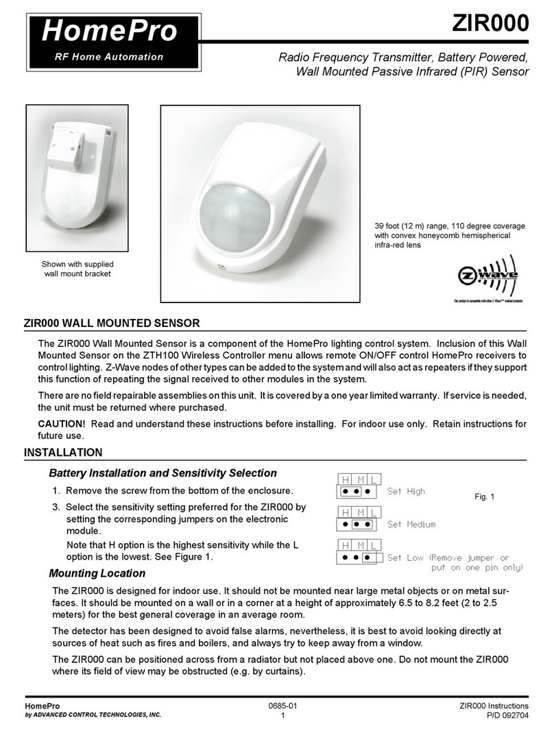
TEST INPUT (EMISSION HALT) FUNCTION
5
When the test input (emission halt input) is turned ON (+1.5V or less,) all
LEDs stop emission, generating the wafer sensed condition, and output
transistors of all channels become ON.
The output circuit of the sensor can be checked by using the test input
(emission halt input.)
Ɣ
Ɣ
ON
OFF
Emission
Emission
halt
ON
[Emitting LED]
[Output]
Normal Error
OFF
Test input
(Emission halt input)
OUTPUT INVALID (EXTERNAL SYNCHRONIZATION) FUNCTION
6
If the output invalid input is turned ON (+1.5V or less,) the output transistors of
all channels stay in the OFF state irrespective of the wafer detection condition.
Several sensors can be used in parallel by using the output invalid inputs,
thereby reducing the required PLC input points.
Ɣ
Ɣ
Output
Output invalid
input 1
Output invalid input 2
Sensor 1Sensor 2
Switch position Sensor operation
1
2Only Sensor 2 is operative
1
2Only Sensor 1 is operative
Connector pin positionƔ
2927252321191715131197531
30282624222018161412108642
Orientation mark
Recommended mating connector
HIF3BA-30D-2.54R
[Manufactured by Hirose Electric Co., LTD.]
Connector
HIF3BA-30PD-2.54R-MC
[Manufactured by Hirose Electric Co., LTD.]
Terminal No.
Description
Terminal No.
Description
1 0V 16 OUT 14
2 +V 17 OUT 15
3 OUT 1 18 OUT 16
4 OUT 2 19 OUT 17
5 OUT 3 20 OUT 18
6 OUT 4 21 OUT 19
7 OUT 5 22 OUT 20
8 OUT 6 23 OUT 21
9 OUT 7 24 OUT 22
10 OUT 8 25 OUT 23
11 OUT 9 26 OUT 24
12 OUT 10 27 OUT 25
13 OUT 11 28
OUT 26 (Note)
14 OUT 12 29
Output invalid input
15 OUT 13 30
Test input (Emission halt input)
Note: Terminal No.28 of M-825 and M-625 is
assigned 0V.
PRINTED IN JAPAN
Overseas Sales Dept. (Head Office)
2431-1 Ushiyama-cho, Kasugai-shi, Aichi, 486-0901, Japan
Phone: +81-(0)568-33-7861 FAX: +81-(0)568-33-8591
Europe Headquarter: Panasonic Electric Works Europe AG
Rudolf-Diesel-Ring 2, D-83607 Holzkirchen, Germany
Phone: +49-8024-648-0
US Headquarter: Panasonic Electric Works Corporation of America
629 Central Avenue New Providence, New Jersey 07974 USA
Phone: +1-908-464-3550
URL : sunx.com
SUNX Limited
SPECIFICATIIONS
7
Type For 8 inch wafer
For 6 inch wafer
25 pieces 26 pieces 25 pieces
Item
Model No.
M-825 M-826 M-625
Wafer pitch 6.35mm 4.76mm
Supply voltage 20 to 26.4V DC Ripple P-P 10% or less
Current consumption 200mA or less
Sensing output
NPN open-collector transistor
Maximum sink current: 20mA
Applied voltage: 30V DC or less
(between sensing output and 0V)
Residual voltage: 1V or less (at 20mA sink current)
•
•
•
Number of channels
25 channels 26 channels 25 channels
Output operation Dark-ON
Response time 1ms or less
Power indicator Red LED (lights up when the power is ON)
Ambient temperature
0 to +40
Û&
(No dew condensation,) Storage: -25 to +60
Û
C
Ambient humidity 35 to 85% RH, Storage: 35 to 85% RH
Emitting element Infrared LED (modulated)
Material Enclosure: ABS, Sensing probe: PPS, Connector: PBT
Cable PPSLWFKFRUHÀH[LEOHÀDWFDEOHPPORQJZLWK
clamp connector
Weight 150g approx.
Accessory Spacer: 2 pcs.
CAUTIONS
8
This product has been developed / produced for industrial use only.
Make sure that the power supply is off while wiring.
Do not run the wires together with high-voltage lines or power lines or put
them in the same raceway. This can cause malfunction due to induction.
Verify that the supply voltage variation is within the rating.
If power is supplied from a commercial switching regulator, ensure that
the frame ground (F.G.) terminal of the power supply is connected to an
actual ground.
In case noise generating equipment (switching regulator, inverter motor,
etc.) is used in the vicinity of this product, connect the frame ground (F.G.)
terminal of the equipment to an actual ground.
Do not use during the initial transient time (100ms.) after the power sup-
ply is switched on.
([WHQVLRQXSWRWRWDOPLVSRVVLEOHZLWKDQHTXLYDOHQWÀDWFDEOH
Make sure that stress by forcible bend or pulling is not applied directly
to the sensor cable joint.
Take care that the sensor is not directly exposed to fluorescent lamp
from a rapid-starter lamp, a high frequency lighting device or sunlight
etc., as it may affect the sensing performance.
Before use the product, make sure to eliminate the static electricity of
the wafer.
Make sure that stress is not applied to the sensor probe.
Wafer which transmits infrared light cannot be detected, since the infra-
red LED is used for the emitting element.
This sensor is suitable for indoor use only.
Avoid dust, dirt, and steam.
Take care that the product does not come in contact with water, oil,
grease, organic solvents, such as thinner, etc., strong acid or alkaline.
Ɣ
Ɣ
Ɣ
Ɣ
Ɣ
Ɣ
Ɣ
Ɣ
Ɣ
Ɣ
Ɣ
Ɣ
Ɣ
Ɣ
Ɣ
Ɣ
INTENDED PRODUCTS FOR CE MARKING
9
The models listed under “ SPECIFICATIONS” come with
CE Marking.
$VIRUDOORWKHUPRGHOVSOHDVHFRQWDFWRXURI¿FH
Ɣ

