System Overview
www.ti.com
6TIDUEN1A–December 2018–Revised August 2019
Submit Documentation Feedback
Copyright © 2018–2019, Texas Instruments Incorporated
3- to 7-VIN, 24-A IOUT, 0.95-VOUT, Space-Grade Current Sharing Point-of-
Load (POL) Reference Design
2.3 Highlighted Products
The following section describes the important ICs that make up the TIDA-070005 24-A solution.
2.3.1 TPS50601A-SP
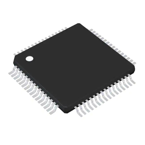
The TPS50601A-SP is a radiation hardened, 7-V, 6-A synchronous step-down converter, which is
optimized for small designs through high efficiency and integrating the high-side and low-side MOSFETs.
The device is offered in an ultra small, thermally enhanced 20-pin ceramic flatpack package.
The output voltage startup ramp is controlled by the SS/TR pin which allows operation as either a stand
alone power supply or in tracking situations. Power sequencing is also possible by correctly configuring
the enable and the open drain power good pins. In addition, the TPS50601A-SP can be configured in
master-slave mode to provide up to 12 A of output current.
Cycle-by-cycle current limiting on the high-side FET protects the device in overload situations and is
enhanced by a low-side sourcing current limit which prevents current runaway. There is also a low-side
sinking current limit which turns off the low-side MOSFET to prevent excessive reverse current. Thermal
shutdown disables the part when die temperature exceeds thermal shutdown temperature.
2.3.2 TPS7A4501-SP
The TPS7A4501-SP is a low-dropout (LDO) regulator optimized for fast-transient response. The 5962-
1222402VHA can supply 750 mA of output current with a dropout voltage of 300 mV. The
5962R1222403VXC can supply 1.5 A of output current with a dropout voltage of 320 mV. Quiescent
current is well controlled; it does not rise in dropout, as with many other regulators. In addition to fast
transient response, the TPS7A4501-SP regulator has very-low output noise, which makes it ideal for
sensitive RF supply applications.
Output voltage range is from 1.21 to 20 V. The TPS7A4501-SP is stable with output capacitance as low
as 10 µF. Small ceramic capacitors can be used without the necessary addition of ESR, as is common
with other regulators. Internal protection circuitry includes reverse-battery protection, current limiting,
thermal limiting, and reverse-current protection. The device is available as an adjustable device with a
1.21-V reference voltage. The 5962-1222402VHA is available in 10-pin CFP (U) package and
5962R1222403VXC is available in thermally-enhanced 10-pin CFP (HKU) package. Known good die
(KGD) option is available for both 5962-1222402V9A for non-RHA version and 5962R1222403V9A for
RHA
2.3.3 INA901-SP
The INA901-SP is a voltage-output, current-sense amplifier that can sense drops across shunt resistors at
common-mode voltages from –16 V to +80 V, independent of the supply voltage. The INA901-SP
operates from a single 2.7-V to 18-V supply, drawing 700 μA (typical) of supply current.
The gain of the INA901-SP is 20 V/V. The 130-kHz bandwidth simplifies use in current-control loops. The
pinouts readily enable filtering.
The device is specified over the extended operating temperature range of –55°C to 125°C and is offered
in an 8-pin CFP package.
2.3.4 SE555-SP
The SE555-SP is a precision timing circuit capable of producing accurate time delays or oscillation. In the
time-delay or monostable mode of operation, the timed interval is controlled by a single external resistor
and capacitor network. In the astable mode of operation, the frequency and duty cycle can be controlled
independently with two external resistors and a single external capacitor.
The threshold and trigger levels normally are two-thirds and one-third, respectively, of VCC. These levels
can be altered by use of the control-voltage terminal. When the trigger input falls below the trigger level,
the flip-flop is set, and the output goes high. If the trigger input is above the trigger level and the threshold
input is above the threshold level, the flip-flop is reset and the output is low. The reset (RESET) input can
override all other inputs and can be used to initiate a new timing cycle. When RESET goes low, the flip-
flop is reset, and the output goes low. When the output is low, a low-impedance path is provided between
discharge (DISCH) and ground.
