4/31
ZYNQ FPGA Development Platform AC7015 User Manual
Amazon Store: https://www.amazon.com/alinx
Part 1: AC7015 Core Board Introduction
The AC7015 (core board model, the same below) core board is an FPGA
development board based on the Zynq chip
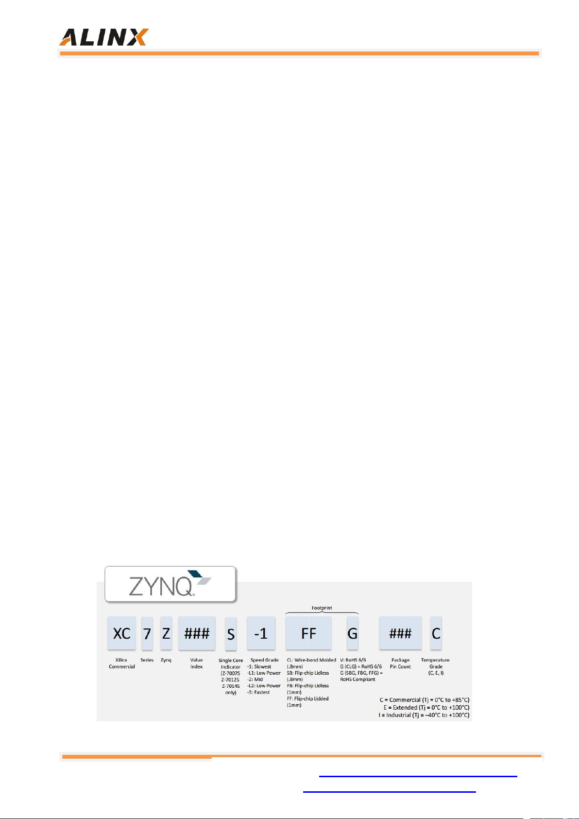
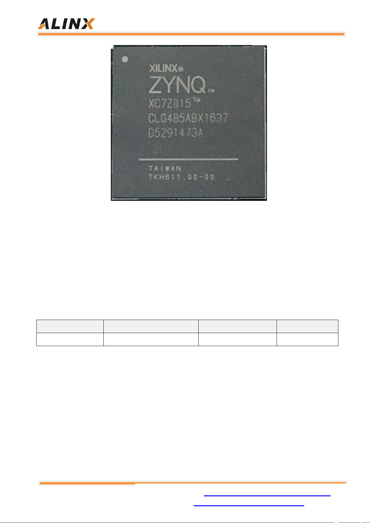
XC7Z015-2CLG485I
of the XILINX
ZYNQ7000 series. The ZYNQ chip's PS system integrates two ARM CortexTM-A9
processors, AMBA® interconnects, internal memory, external memory interfaces
and peripherals. The ZYNQ FPGA chip contains a wide range of programmable
logic cells, DSP and internal RAM.
The core board uses two SK Hynix DDR3 chips (H5TQ4G63AFR-PBI), each
with a DDR capacity of 4Gbit; two DDR chips form a 32-bit data bus width, and the
read and write data clock frequency between ZYNQ FPGA and DDR3 is up to
533Mhz; such a configuration can meet the system's high bandwidth data
processing needs
In order to connect to the expansion board, the four board-to-board connectors
of the core board extend the USB interface of the PS side, the Gigabit Ethernet
interface, the SD card interface and other remaining MIO ports. Extend ZynQ's 4-
pair high-speed transceiver GTP interface. Almost all IO ports (84) of BANK13,
BAN34 and BANK35 on the PL side, the level of IO of BANK35 can be modified by
replacing the LDO chip on the core board to meet the requirements of users with
different level interfaces. For users who need a lot of IOs, this core board will be a
good choice. Moreover, the IOs connection part, the routing between the ZYNQ
FPGA chip and the interface is equal length and differential processing. The core
board size is only 60*60 (mm), which is very suitable for secondary development.