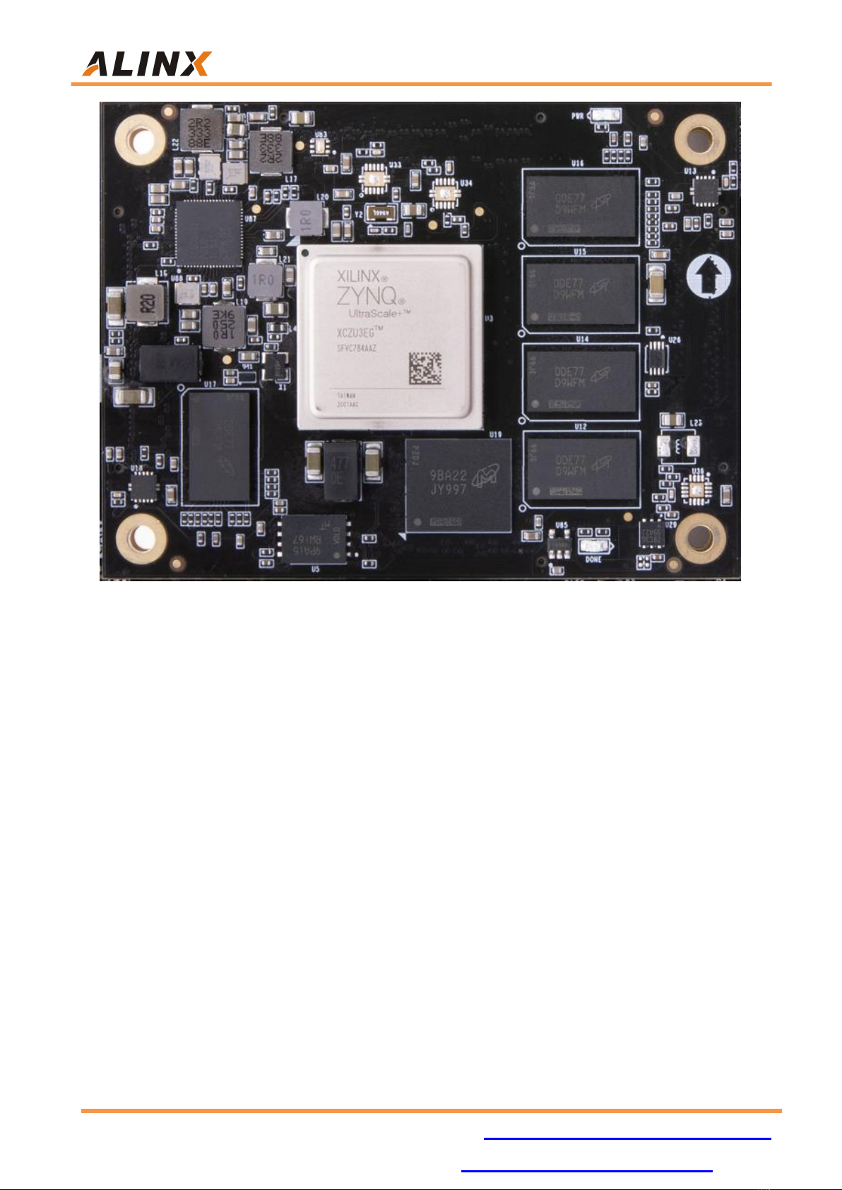
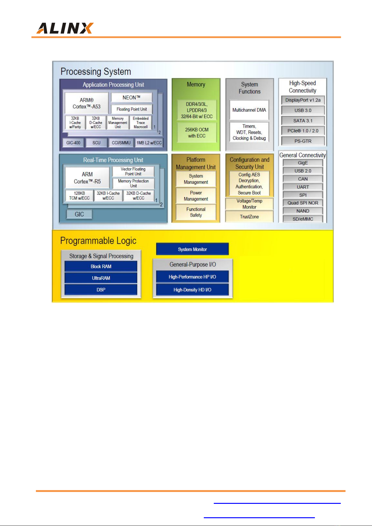
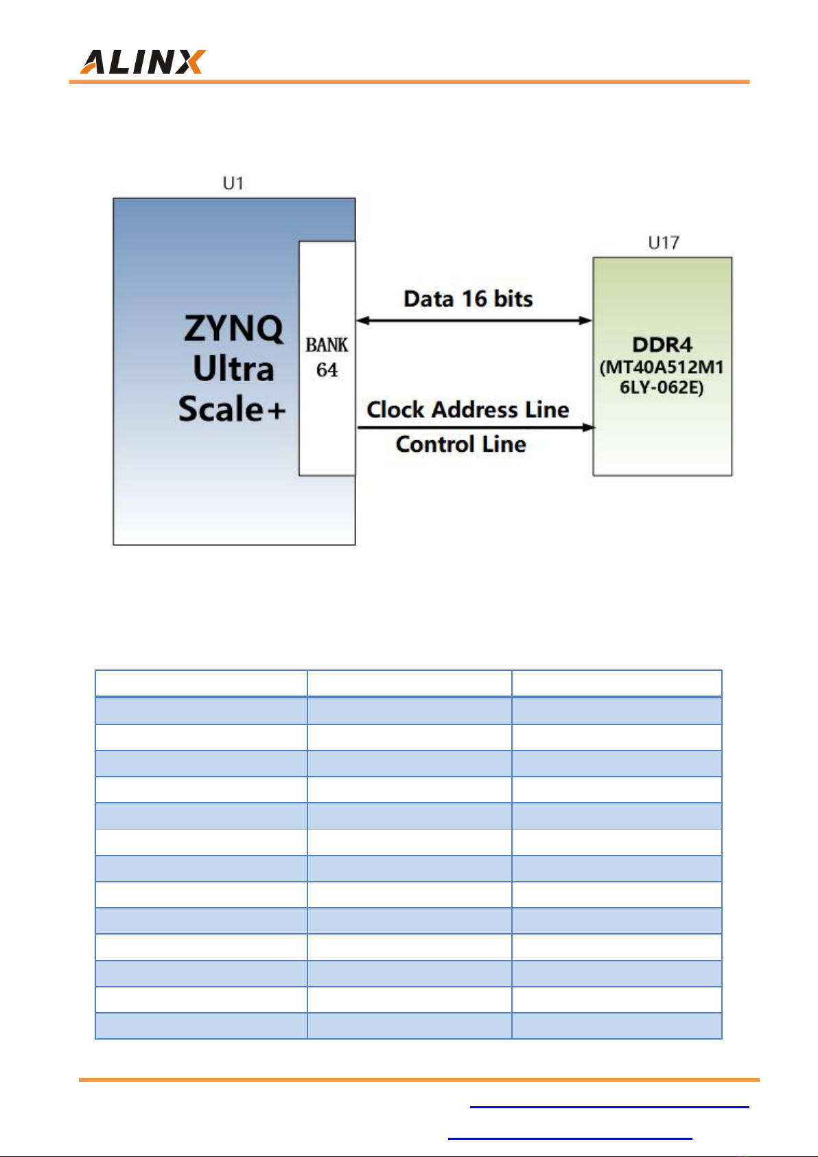
Alinx ACU3EG User manual
Other Alinx Motherboard manuals

Alinx
Alinx AX7103 User manual

Alinx
Alinx ARTIX-7 FPGA User manual

Alinx
Alinx ACU7EVB User manual

Alinx
Alinx ACU15EG User manual

Alinx
Alinx AX7021 User manual

Alinx
Alinx AC7021B User manual

Alinx
Alinx AC7021 User manual

Alinx
Alinx ZYNQ7000 FPGA User manual

Alinx
Alinx Cyclone IV FPGA User manual

Alinx
Alinx KINTEX-7 FPGA User manual

Alinx
Alinx ARTIX-7FPGA User manual

Alinx
Alinx ARTIX-7 FPGA User manual

Alinx
Alinx KINTEX UltraScale FPGA AXKU042 User manual

Alinx
Alinx ZYNQ UltraScale+ AXU5EV-E User manual

Alinx
Alinx ZYNQ7000 FPGA User manual

Alinx
Alinx AX301 User manual

Alinx
Alinx AV4075 User manual

Alinx
Alinx AC7015 User manual

Alinx
Alinx AC7Z035B User manual

Alinx
Alinx ZYNQ7000 FPGA User manual