3
DEMO MANUAL DC2611A
Rev. 0
DC2611A RECONFIGURATION
The following covers the hardware reconfiguration of the
DC2611A. Refer to LTC6955 data sheet for a better under-
standing of device specific considerations.
Power Supply Options
Table2 provides the power supply options for DC2611A.
By default the DC2611A is setup to use the single supply
option. However, a dual supply option is available to power
the higher current supply from our Silent Switcher, such
as the LT8609S. The Silent Switcher improves the power
efficiency over the low noise LDO. A spurious free supply,
such as a low noise LDO, is required on the LTC6955’s
VIN+supply pin.
Table2. Power Supply Options
Power Supply Voltage/Current
(Recommended Supply)
DEFAULT OPTION R18 J27 (3.3V) E10 (VIN33)
x Single
Supply
Installed 3.3V/750mA
(Low Noise LDO)
NA
Dual
Supply
Do Not
Install
3.3V/750mA
(Silent Switcher)
3.3V/150mA
(Low Noise LDO)
Input Termination Options
Table3 provides the single-ended and differential input
termination options. By default the DC2611A is setup for
a single-ended input on the IN–SMA (J25). For best per-
formance different termination networks are provided for
input signals <5GHz and input signals >5GHz.
LTC6955-1 Divide by Two Coupling Spur
To help reduce the LTC6955-1’s OUT10 /2 coupling spur
to other outputs a ferrite bead (FB1) should be installed
on the OUT10 supply pin, VOUT+ (Pin 5). For the LTC6955
FB1 should be a 0Ω resistor.
CML Outputs, OUT[10:0]
The DC2611A has 11 CML outputs. Six of these outputs
are AC-coupled and brought out to SMAs (OUT10, OUT8,
OUT6, OUT4, OUT1 or OUT0). To drive 50Ω impedance
instruments connect OUTx+ to the instrument and OUTx–
to a 50Ω termination, or vice versa.
The remaining five outputs (OUT9, OUT7, OUT5, OUT3,
and OUT2) are terminated with a 100Ω resistor on board.
To connect these outputs to a 50Ω instrument, remove
the 100Ω termination, and install the appropriate SMAs
and AC blocking capacitors.
Refer to LTC6955 data sheet for differential termination
options.
Alternate Configuration Options
To take advantage of the LTC6955’s maximum output
frequency and ultralow output additive phase noise,
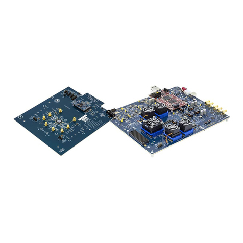
the DC2611A (LTC6955, LTC6955-1), the DC2609A
(LTC6952) and the VCO rider board (DC2664A) were
designed to mate directly together, as shown in Figure2.
This setup allows for options to lock the LTC6952 refer-
ence input to:
A) A <7.5GHz VCO and LTC6955-1 output frequency, by
utilizing the LTC6955-1 divide by two output on OUT10
to drive the LTC6952 VCO input. (refer to Figure2)
B) Any VCO and create lower jitter clocks from a LTC6955
or LTC6955-1 output than a standalone LTC6952
produces.
Refer to the LTC6952 and LTC6955 data sheet’s typical
application for measured results. Refer to the DC2664A
demo manual for recommendation on loop filter compo-
nent placement.
Table3. Input Termination Options (*)
DEFAULT TERMINATION R8 (Ω) R9 (Ω) R10 (Ω) R11 (Ω) R19 (Ω) R20 (Ω) C58 C59 C60 C61
DC2611A-A SE, IN–, <5GHz 75 DNI 30 DNI DNI DNI 0.1uF 0.1uF DNI 0.1uF
DC2611A-B SE, IN–, ≥5GHz DNI DNI DNI 1nH DNI 49.9 DNI 1pF 1pF DNI
SE, IN+, <5GHz 30 DNI 75 DNI DNI DNI 0.1uF DNI 0.1uF 0.1uF
SE, IN+, ≥5GHz DNI DNI DNI 1nH 49.9 DNI DNI 1pF 1pF DNI
DIFF, CML or PECL, <5GHz DNI 160 DNI DNI DNI DNI DNI 0.1uF 0.1uF DNI
DIFF, CML or PECL, ≥5GHz DNI DNI DNI 1nH DNI DNI DNI 1pF 1pF DNI
DIFF, LVDS DNI DNI DNI 160 DNI DNI DNI 0.1uF 0.1uF DNI
*SE = Single-Ended, DIFF = Differential, DNI = Do Not Install
