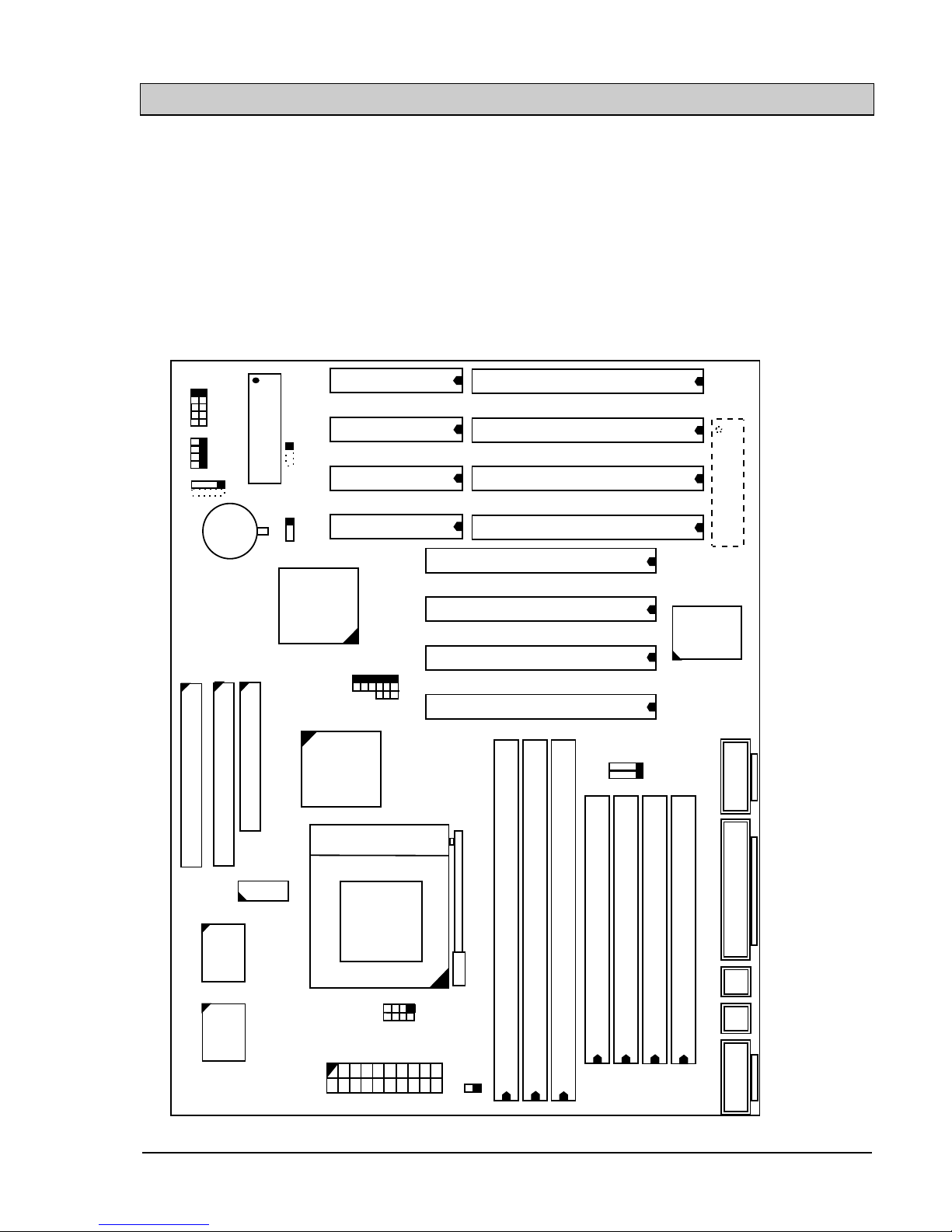
PT-5ITA SYSTEM BOARD HARDWARE SETUP
4-2
SIMMs' and DIMM's operating voltage :
(1) SIMM1 - SIMM4 : + 5V DC
(2) DIMM1 - DIMM3 : +3.3V DC.
DRAM Bank can be populated in any order (bank 0 does not have to be populated
before bank 2).Within any given bank, the SIMMs must be the same size. Among the
three banks, SIMM (DIMM) densities can be mixed in any order. EDO, FPM and
SDRAMs can be mixed between SIMMs (DIMM), a given SIMM (DIMM) must
contain only one type of DRAM. When DRAM types are mixed each SIMM (DIMM)
runs optimized for that particular type of DRAM.
There is no jumper needed for DRAM configuration, DRAMs' type and size will be
detected by system BIOS automatically.
The following table provides the possible combinations for DRAM memory
installation.
Bank 0 Bank 1 Bank 2
SIMM1 - 2 DIMM1 SIMM3 - 4 DIMM2 DIMM3
Single-sided Empty Single-sided Empty Empty
Double-sided Empty Double-sided Empty Empty
Empty Single-sided Empty Single-sided Single-sided
Empty Double-sided Empty Double-sided Double-sided
Note : We strongly recommend, Don't install 5V SIMM module and 3.3V DIMM
modules at the same time.
4.2.2 L2 CACHE MEMORY INSTALLATION
The PT-5ITA system board will support 256KB or 512KB cache memory on board,
using synchronous pipeline-burst SRAMs. Both Write Back and Write Through cache
update policy are supported.
The following table lists the detailed combination about cache memory installation.
Cache Size Data SRAMs(U16 or U17) Tag SRAMs(U14)
256 KB 32KB x 64 8KB or 16KB or 32KB x 8
512 KB 64KB x 64 16KB or 32KB x 8