ECS P6VPA2 User manual
i
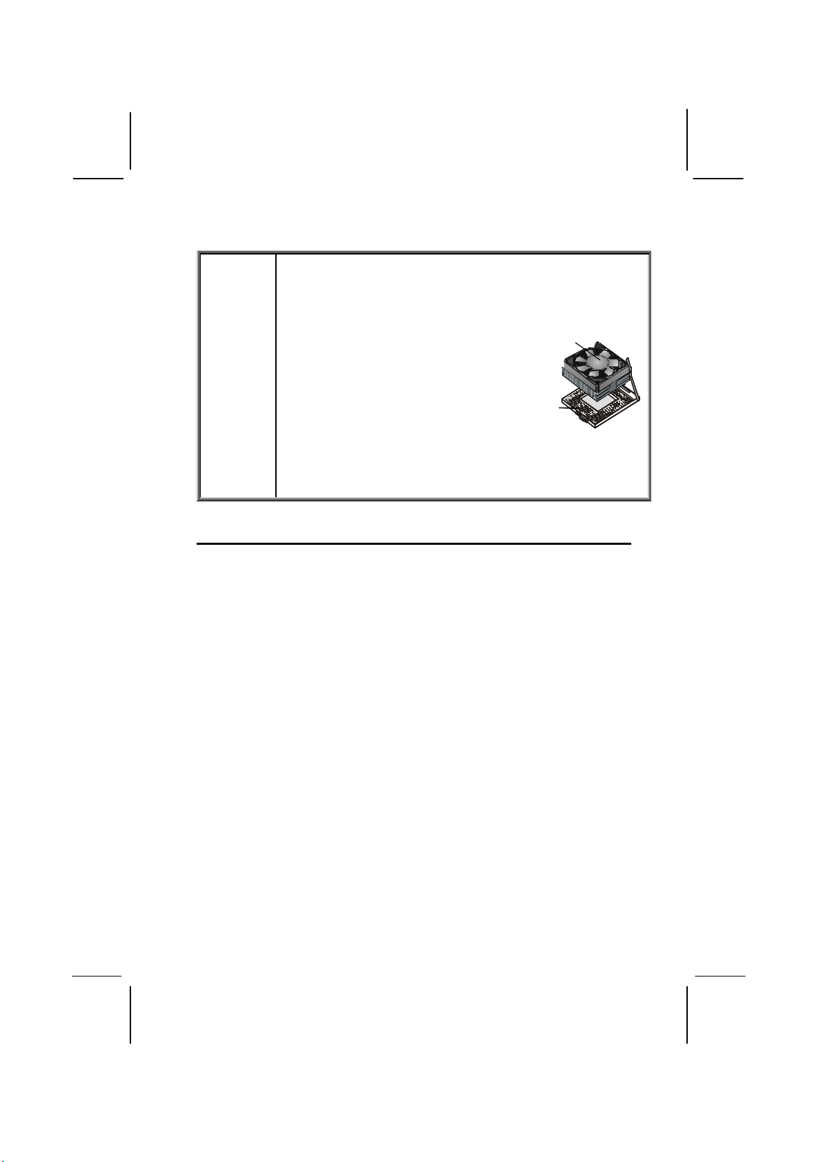
Caution! When installing a CPU heatsink and
cooling fan make sure that you DO NOT
scratch the motherboard or any of the
surface-mount resistors with the clip of
the cooling fan. If the clip of the cooling
fan scrapes across the mainboard, you
may cause serious damage to both the
mainboard and the processor.
On most mainboards, there are small
surface-mount resistors near the
processor socket, which may be damaged
if the cooling fan is carelessly installed.
Avoid using cooling fans with sharp
edges on the fan casing and the clips.
Also, install the cooling fan in a well-lit
work area so that you can clearly see the
mainboard and processor socket.
Cooling fan and
heat sink
CPU socket
Important Information
Copyright
This publication, including all photographs, illustrations and
software, is protected under international copyright laws, with all
rights reserved. Neither this manual, nor any of the material
contained herein, may be reproduced without the express
written consent of the manufacturer.
Version 1.0
Disclaimer
The information in this document is subject to change without
notice. The manufacturer makes no representations or
warranties with respect to the contents hereof and specifically
disclaims any implied warranties of merchantability or fitness for
any particular purpose. Further, the manufacturer reserves the
right to revise this publication and to make changes from time to
time in the content hereof without obligation of the manufacturer
to notify any person of such revision or changes.

ii
Trademark Recognition
Microsoft, MS-DOS and Windows are registered trademarks of
Microsoft Corp.
MMX, Pentium, Pentium-II, Pentium-III, Celeron are registered
trademarks of Intel Corporation.
Other product names used in this manual are the properties of
their respective owners and are acknowledged.
Federal Communications Commission (FCC)
This equipment has been tested and found to comply with the
limits for a Class B digital device, pursuant to Part 15 of the FCC
Rules. These limits are designed to provide reasonable protection
against harmful interference in a residential installation. This
equipment generates, uses, and can radiate radio frequency
energy and, if not installed and used in accordance with the
instructions, may cause harmful interference to radio
communications. However, there is no guarantee that interference
will not occur in a particular installation. If this equipment does
cause harmful interference to radio or television reception, which
can be determined by turning the equipment off and on, the user
is encouraged to try to correctthe interference by one or more of
the following measures:
qReorient or relocate the receiving antenna.
qIncrease the separation between the equipment and the
receiver.
qConnect the equipment onto an outlet on a circuit
different from that to which the receiver is connected.
qConsult the dealer or an experienced radio/TV technician
for help.
Shielded interconnect cables and a shielded AC power cable
must be employed with this equipment to ensure compliance
with the pertinent RF emission limits governing this device.
Changes or modifications not expressly approved by the
system’s manufacturer could void the user’s authority to operate
the equipment.

iii
Declaration of Conformity
This device complies with part 15 of the FCC rules. Operation is
subject to the following conditions:
qThis device may not cause harmful interference, and
qThis device must accept any interference received,
including interference that may cause undesired
operation.
Canadian Department of Communications
This class B digital apparatus meets all requirements of the
Canadian Interference-causing Equipment Regulations.
Cet appareil numérique de la classe B respecte toutes les
exigences du Réglement sur le matériel brouilieur du Canada.

iv
About the Manual
The manual consists of the following chapters:
Introduction
Use the Introduction Chapter to learn about the features of the
mainboard, and verify the checklist of items that are shipped
with the package.
Installation
Use the Installation Chapter to learn how to install the
mainboard and get your system up and running.
Setup
Use the Setup Chapter to configure the mainboard for optimum
performance.
Software
Use the Software Chapter to learn how to install the software
drivers and support programs that are provided with this
mainboard.

v
Contents
Important Information i
Copyright i
Disclaimer i
Trademark Recognition ii
Federal Communications Commission(FCC) ii
Declaration of Conformity iii
Canadian Department of Communications iii
About the Manual iv
CHAPTER 1: INTRODUCTION 1
Welcome 1
Checklist 2
Recommendations 3
Features 4
CHAPTER 2: INSTALLATION 7
Quick Installation Table 7
Before You Begin 8
Static Electricity 8
Choosing a Case 9
Preparing the Mainboard 10
Mainboard Guide 10
I/O Ports Side View 12
How to Set Jumpers 13
Check the Jumper Settings 14
Installing the Mainboard in a Case 17
Connecting Internal Components 18
Installing Other Hardware 20
Installing the Processor 20
Install the Memory Modules 22
Installing a Hard Disk Drive and CD-ROM 24
Installing a Floppy Diskette Drive 27
Using the Expansion Slots 28
Add-in Card Options 31

vi
Making External Connections 33
External Connector Color Coding 34
CHAPTER 3: SETUP 35
About the Setup Utility 35
Entering the Setup Utility 36
BIOS Navigation Keys 37
Using BIOS 38
How to Flash a New BIOS 39
Standard CMOS Setup Option 40
Advanced CMOS Setup Option 43
Advanced Chipset Features Option 46
Integrated Peripherals Option 51
Power Management Setup Option 57
PNP/PCI Configuration Option 62
PCI Health Status Option 64
Frequency Control Option 65
Load Fail-Safe Defaults Option 66
Load Optimized Defaults Option 66
Set Supervisor and User Passwords Options 67
Save & Exit Setup Option 68
Exit Without Saving Option 68
CHAPTER 4: SOFTWARE 69
Auto-installing under Windows 98 70
Folders for this Mainboard 73
Utility Folder Installation Notes 74
Mainboard (P6VPA2) Installation Notes 75
Audio Software 75
IDE Software 76
APPENDIX: JUMPER SETTING REFERENCE 77
Quick Jumper Setting Reference 77

1
C
Ch
ha
ap
pt
te
er
r
1
1:
:
I
In
nt
tr
ro
od
du
uc
ct
ti
io
on
n
Welcome
Congratulations on purchasing the P6VPA2 mainboard. The
P6VPA2 mainboard is an ATX mainboard that uses a 4-layer
printed circuit board and measures 222 mm x 304 mm. The
mainboard features a Socket 370 that accommodates Celeron,
FC-PGA Pentium III, and Cyrix III processors that support
frontside bus (FSB) speeds up to 133 MHz. The P6VPA2
features the VIA Apollo Pro266 chipset which combines support
for the new high-bandwidth Double Data Rate (DDR) 266
SDRAM with a high-speed V-Link Hub Architecture, and the AC
97 audio codec.
Note: SDRAM provides 800 MBps or 1 GBps data transfer
depending on whether the bus is 100 MHz or 133 MHz. Double
Data Rate SDRAM (DDR SDRAM) doubles the rate to 1.6 GBps
or 2.1 GBps by transferring data on both the rising and falling
edges of the clock. DDR SDRAM uses additional power and
ground lines and requires 184-pin DIMM modules rather than the
168-pin DIMMs used by SDRAM.
The mainboard delivers high-level performance witha 4xAGP
(Accelerated Graphics Port) slot and two Ultra DMA (UDMA)
ports that support up to four ATAPI (AT Attachment Packet
Interface) devices. The PCI IDE also supports PIO Mode 3 and
4, UDMA33/66/100 IDE, and an ATAPI CD-ROM.
The mainboard accommodates DDR200/DDR266 or
PC1600/PC2100 DDR SDRAM (Double Data Rate Synchronous
DRAM) up to 3 GB using three 2.5V unbuffered DIMM modules.
The P6VPA2 also has a full set of I/O ports, such as dual channel
IDE interfaces, a floppy controller, two FIFO serial port connectors,
an EPP/ECP-capable bi-directional parallel port connector, a dual
USB (Universal Serial Bus) connector, and PS/2 keyboard and
mouse connectors.

2
One AGP slot, five PCI local bus slots, one Communications
Network Riser (CNR) slot, and one Advanced Communication
(ACR) slot provide expandability for add-on peripheral cards.
This chapter contains the following information:
qChecklist comprises a list of the standard and optional
components that are shipped with this mainboard
qRecommendationslists some Do’s and Don’ts from the
manufacturer to help ensure reliability and performance
from this product
qFeatures highlights the functions and components that
make this one of the best value mainboards on the
market
Checklist
Compare the contents of your mainboard package with the
standard checklist below. If any item is missing or appears
damaged, please contact the vendor of your mainboard package.
Standard Items
qOne P6VPA2 mainboard
qOne diskette drive ribbon cable and bracket
qOne IDE drive ribbon cable and bracket
qThis user’s manual
qSoftware support CD-ROM disc

3
Recommendations
This mainboard automatically determines the CPU clock
frequency and system bus frequency for the kind of processor
that you install. You may be able to change these automatic
settings by changing the settings in the system Setup Utility. We
strongly recommend that you do not overclock the mainboard to
run processors or other components faster than their rated
speed.
Warning: Overclocking components can adversely affect the
reliability of the system and introduce errors into your system.
Overclocking can permanently damage the mainboard by generating
excess heat in components that are run beyond the rated limits.
Components on this mainboard can be damaged by discharges
of static electricity. Handle the board carefully holding it by the
edges. Don’t flex or stress the circuit board. Keep the board in
its static-proof packing until you are ready to install it. Follow the
static guidelines given at the beginning of Chapter 2.

4
Features
The key features of this mainboard are the wide range of
processors that can be installed, and the high level of integration.
Value-class Processors
Functioning as a platform for a value PC, the P6VPA2 features a
Socket 370 that accommodates Intel Celeron, FC-PGA Pentium
III, and VIA Cyrix III processors. The P6VPA2 supports
66/100/133 MHz FSB speeds.
VIA Apollo Pro266 Chipset
The VIA Apollo Pro266 chipset is based on an innovative and
scaleable architecture with proven reliability and performance.
The Apollo Pro266 is consists of the VT8633 V-Link Host system
controller (NB) and the VT8233 V-Link client PCI/LPC bridge
Controller.
Using an advanced V-Link memory controller architecture, the
VIA Apollo Pro266 chipset supports up to 3.0 GB of the latest
high-speed DDR200/266 SDRAM. These advanced memory
technologies provide the bandwidth and performance necessary
for even the most demanding Internet and 3D graphics. The low
2.5-volt power consumption of the DDR266 SDRAM makes it an
excellent solution for notebooks and desktops with a small
footprint. The Apollo Pro266 is configured with a 133 MHz
frontside bus, optimizing the performance of the latest Pentium
and Cyrix processors, and Celeron processors running at 66/100
MHz FSB speed.
The Apollo Pro266 supports a 4xAGP interface providing vivid
3D graphics and video performance. The ATA 100 interface on
the chipset helps boost system performance by providing a high-
speed connection to ATA 100 Hard Disk Drives, delivering
maximum sustained data transfer rates of 100 MB/sec.
Additional key features include support for six USB ports, AC-97
link for audio and modem, hardware monitoring, and
ACPI/OnNow power management.

5
Inexpensive Memory
The board has three DIMM sockets for the installation of 184-pin,
2.5 non-buffered DIMM memory modules. The DIMM memory
modules must be DDR SDRAM memory chips.
4xAGP Graphics Adapter Slot
P6VPA2 includes a 4xAGP slot that provides four times the
bandwidth of the original AGP specification. AGP technology
provides a direct connection between the graphics sub-system
and the processor so that the graphics do not have to compete
for processor time with other devices on the PCI bus.
AC 97 Audio Codec
The AC 97 Audio codec is compliant with the AC 97 2.1
specification, and supports 18-bit ADC (Analog Digital Converter)
and DAC (Digital Analog Converter) resolution as well as 18-bit
stereo full-duplex codec with independent and variable sampling
rates. Further features include support for four analog line-level
stereo inputs.
Expansion Options
Five 32-bit PCI slots, an 4xAGP slot, a Communications
Network Riser (CNR) slot, and an Advanced Communications
Riser (ACR) slot provide plenty of expansion potential. The
P6VPA2 support Ultra DMA33/66/100 bus mastering with
transfer rates up to 33/66/100 MB/sec.
Integrated I/O
The mainboard has a full set of I/O ports and connectors. The
I/O template on the backplane includes two PS/2 ports for
mouse and keyboard, two serial ports, one parallel port, one
MIDI/game port, two USB ports, and audio jacks for microphone,
line-in and line-out. The board includes two IDE channels and a
floppy disk drive interface.
Keyboard Power on Feature
Using the system BIOS setup program, you can configure the
system to turn on using a keyboard-typed password.

6
ProgrammableFirmware
The mainboard includes Award BIOS that allows BIOS setting of
CPU parameters. This fully programmable firmware enhances
the system features and allows users to set such items as power
management, CPU and memory timing, and modem wake-up
alarms. The firmware can also be used to set parameters for
different processor clock speeds.
This concludes Chapter 1. The next chapter will cover installing
and building a working system.

7
C
Ch
ha
ap
pt
te
er
r
2
2:
:
I
In
ns
st
ta
al
ll
la
at
ti
io
on
n
Quick Installation Table
This chapter explains how to successfully install the mainboard
into a computer case and build a working system.
The installation procedure is as follows:
Before you
Begin Provides advice on choosing a case,
avoiding static electricity damage, and
setting jumpers.
Preparing the
Mainboard Provides a guide to the mainboard and I/O
port locations, full details on the jumper
settings, and advice on installing the
mainboard in the system case.
Installing Other
Hardware Provides guidance on installing essential
hardware: processor, memory, hard disk
drive, CD-ROM, floppy disk drive, and
expansion cards.
Making
External
Connections
Provides advice on using the external I/O
ports to install peripheral devices such as a
keyboard, a monitor, a mouse, a printer,
and loudspeakers.
Appendix The Appendix provides a quick reference
for the jumper settings on this mainboard.

8
Before You Begin
Before you begin to install your mainboard, take care not to
damage the product from static electricity. Ensure too that you
are installing the mainboard into a suitable case.
Static Electricity
In adverse conditions, static electricity can accumulate and
discharge through the integrated circuits and silicon chips on this
product. These circuits and chips are sensitive and can be
permanently damaged by static discharge.
•If possible, wear a grounding wrist strap clipped to a
safely grounded device during the installation.
•If you don’t have a wrist strap, discharge any static by
touching the metal case of a safely grounded device
before beginning the installation.
•Leave all components inside their static-proof bags until
they are required for the installation procedure.
•Handle all circuit boards and electronic components
carefully. Hold boards by the edges only. Do not flex or
stress circuit boards.

9
Choosing a Case
The mainboard complies with the specifications for the ATX
system case. Some features on the mainboard are implemented
by cabling connectors on the mainboard to indicators and
switches on the system case. Ensure that your case supports all
the features required. The mainboard can support one or two
floppy diskette drives and four enhanced IDE drives. Ensure that
your case has sufficient power and space for all the drives that
you intend to install.
The mainboard has a set of I/O ports on the rear edge. Ensure
that your case has an I/O template that supports the I/O ports
and expansion slots.
10
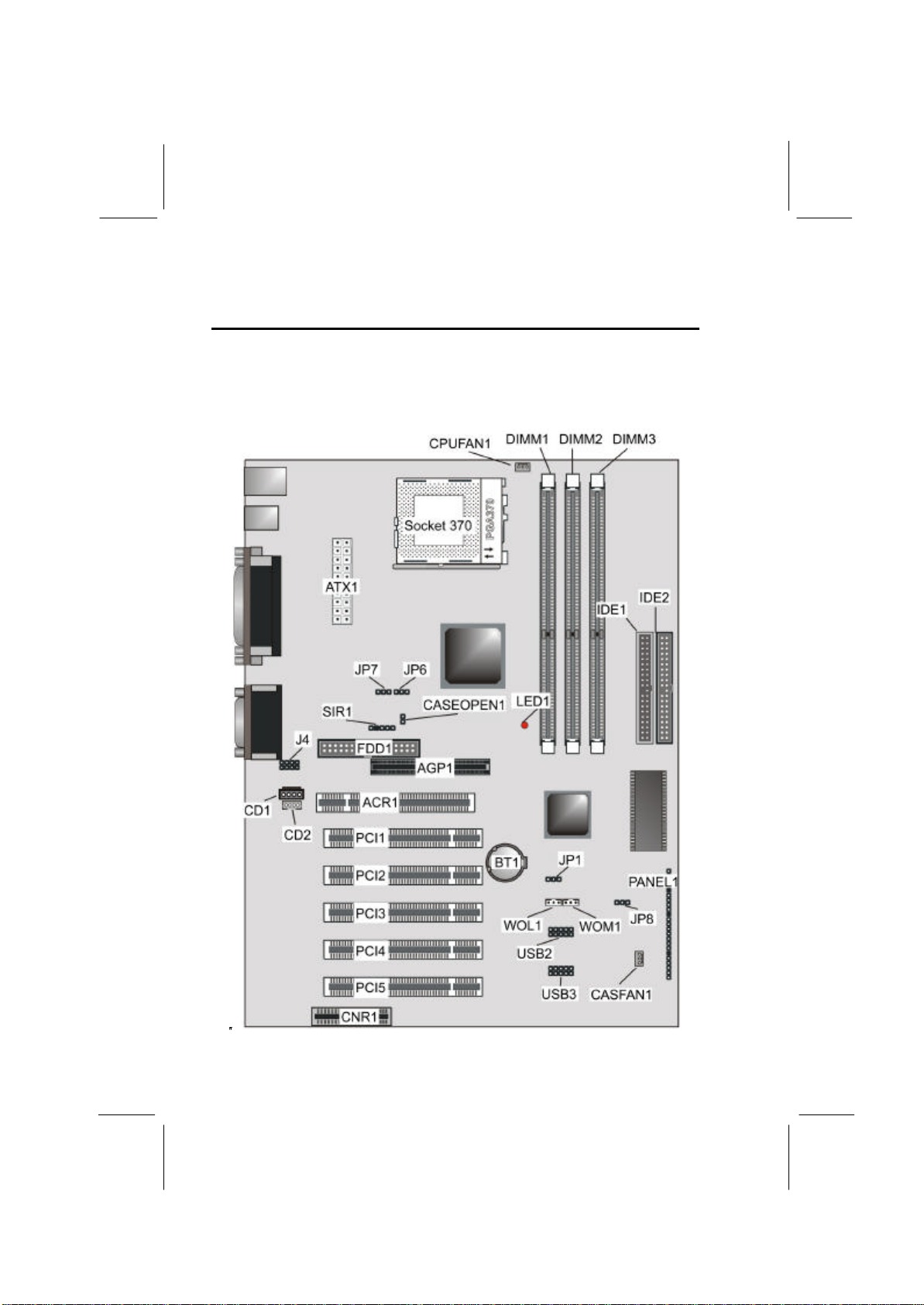
Preparing the Mainboard
Mainboard Guide
Use the following illustration and key to identify the components
on your mainboard.
LTI1
PWRFAN1JP2VGA1PPGA1PWRFAN1CPUFAN1ATX1
LTI1
PWRFAN1JP1JP2VGA1PPGA1DIMM1PWRFAN1CPUFAN1ATX1
11
Key to Mainboard Components
Component Description
CPUFAN1 Power connector for CPU cooling fan
DIMM 1, 2, 3 Three slots for 184-pin DRAM memory module
ATX1 Connector for ATX power supply
Socket 370 CPU socket
IDE1, IDE2 Primary and secondary IDE channels
LED1 Voltage Indicator for DDR DIMM socket
CASEOPEN1 Case open jumper
JP6, 7 CPU frequency select jumper
SIR1 SIR connector for infrared
FDD1 Connector for floppy disk drives
AGP1 Accelerated Graphics Port slot
J4 Extra MIC/line-out header
CD1 Audio connector for CD-ROM/DVD drive
CD2 Auxiliary connector for CD-ROM/DVD drive
ACR1 Advanced Communication Rise (ACR) slot
PCI1 ~ PCI5 Five 32-bit PCI slots
CNR1 Communications Networking Riser slot
BT1 3.3 volt battery for realtime clock
JP1 Clear the system CMOS jumper
WOL1 Connector for LAN wake up
WOM1 Connector for modem wake up
JP8 BIOS Flash protect jumper
USB2/USB3 Extra USB port headers
CASFAN1 Power connector for case cooling fan
PANEL1 Panel connector for switches and indicators
Note: LED1 –This red indicator warns you that the computer is
still powered on and you should not install or uninstall memory
modules.

12
I/O Ports Side View
PS/2
mouse
PS/2
keyboard USB
ports
Parallel port (LPT1)
Serial port
COM 1 Serial port
COM 2 Line-in
Game port
Microphone
Line-out
Key to I/O Ports
Component Description
PS/2 mouse PS/2 port for pointing device (upper port)
PS/2 keyboard PS/2 port for keyboard (lower port)
USB ports Two stacked Universal Serial Bus ports
LPT1 External parallel port
COM1 External serial port COM 1
COM2 External serial port COM 2
Game port External MIDI/game port
Audio ports Audiojacksfor(fromlefttoright)lineout, line
in, microphone

13
How to Set Jumpers
A jumper consists of two or more pins mounted on the
mainboard. Some jumpers might be arranged in a series with
each pair of pins numbered differently. Jumpers are used to
change the electronic circuits on the mainboard. When a jumper
cap (or shunt) is placed on two jumper pins, the pins are SHORT.
If the jumper cap is removed (or placed on just a single pin), the
pins are OPEN.
Short
Open
This illustration shows a 2-pinjumper.
When the jumper cap is placed on
both pins, the jumper is SHORT. If
you remove the jumper cap, or place
the jumper cap on just one pin, the
jumper is OPEN.
This illustration shows a 3-pinjumper.
The jumper cap is placed on pins 2
and 3, so this jumper setting is
SHORT PINS 2-3.
This illustration shows the same 3-pin
jumper. The jumper cap is placed on
pins 1 and 2, so this jumper setting is
SHORT PINS 1-2.
In this manual, all the jumper illustrations clearly show the pin
numbers. When you are setting the jumpers, make sure that the
jumper caps are placed on the correct pins to select the function
or feature that you want to enable or disable.
14
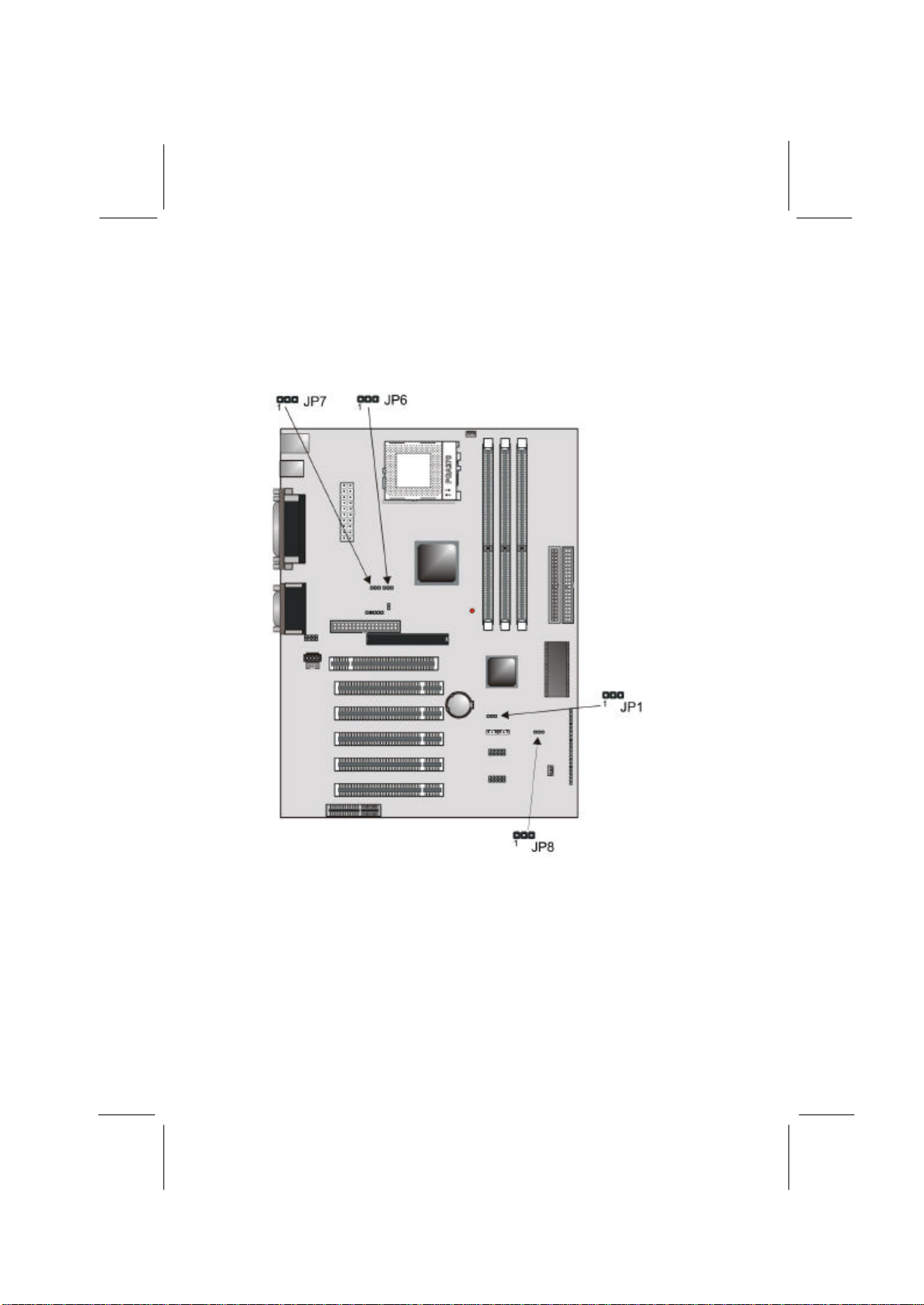
Check the Jumper Settings
Check the mainboard jumpers to ensure that the board is
configured correctly.
JP1: Clear CMOS jumper
Use this jumper to clear the contents of the CMOS memory. You
may need to clear the CMOS memory if the settings in the BIOS
Setup Utility are incorrect and are preventing your mainboard
from operating. To clear the CMOS memory, disconnect all the
power cables from the mainboard and then move the jumper cap
into the Clear CMOS memory setting for a few seconds. CMOS
is cleared.
Other manuals for P6VPA2
1
Table of contents
Other ECS Motherboard manuals


