QUICK START GUIDE
EPC – EFFICIENT POWER CONVERSION CORPORATION | WWW.EPC-CO.COM | COPYRIGHT 2014 | | PAGE 3
EPC9037/37/41
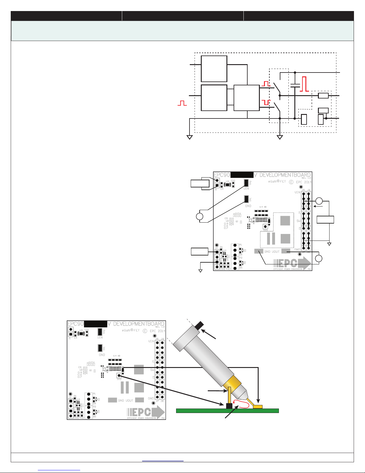
THERMAL CONSIDERATIONS
The EPC9036/37/41 development boards showcase the EPC2100/1/5
eGaNIC. These development boards are intended for bench evalua-
tion with low ambient temperature and convection cooling. The ad-
dition of heat-sinking and forced air cooling can signicantly increase
Figure 4: EPC9036Typical Waveforms forVIN = 12V to 1.2 V/25 A (1000 kHz) Buck converter
showing rising and falling edges, CH4: (VOUT) Switch node voltage
650 ps rise time
ps fall time
the current rating of these devices, but care must be taken to not
exceed the absolute maximum die temperature of 150°C.
NOTE. These development boards do not have any current or thermal protection on
board.
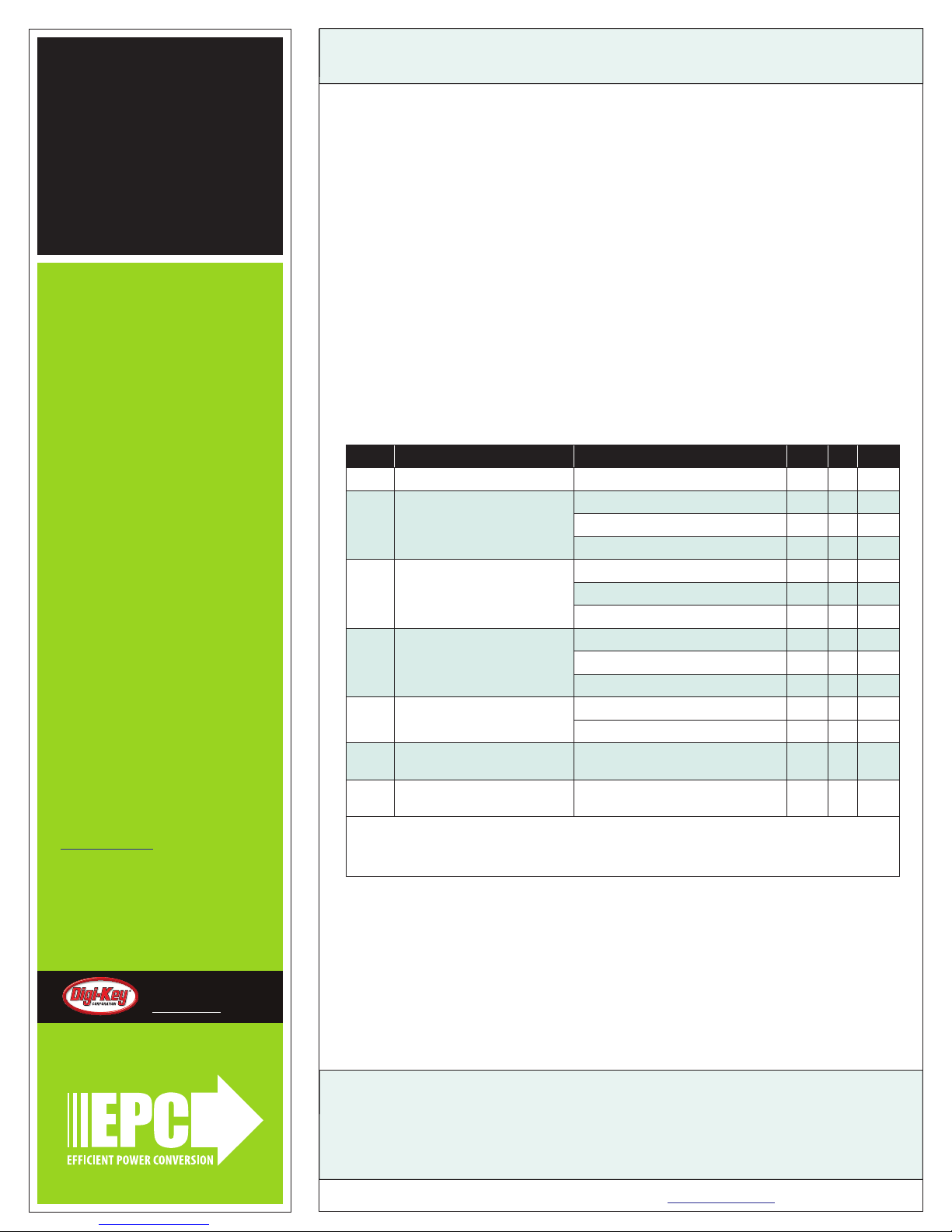
Item Qty Reference Part Description Manufacturer
1 3 C4, C10, C11, Capacitor, 1µF, 10%, 25 V, X5R Murata, GRM188R61E105KA12D
2 2 C16, C17 Capacitor, 100pF, 5%, 50 V, NP0 Kemet, C0402C101K5GACTU
3 2 C9, C19 Capacitor, 0.1µF, 10%, 25 V, X5R TDK, C1005X5R1E104K
4 4 C21, C22, C23, C24 Capacitor - See Table 3 See Table 3
5 2 D1, D2 Schottky Diode, 30 V Diodes Inc., SDM03U40-7
6 3 J1, J2, J9 Connector 2 pins of Tyco, 4-103185-0
7 6 J3, J4, J5, J6, J7, J8 Connector FCI, 68602-224HLF
8 1 Q1 eGaNIC , - see Table 3 See Table 3
9 1 R1 Resistor, 10.0K, 5%, 1/8 W Stackpole, RMCF0603FT10K0
10 2 R2, R15 Resistor, 0 Ohm, 1/8W Stackpole, RMCF0603ZT0R00
11 1 R4 Resistor, 47 Ohm, 1%, 1/8W Stackpole, RMCF0603FT47R0
12 1 R5 Resistor, - see Table 3 See Table 3
13 4 R19, R20, R23, R24 Resistor, 0 Ohm, 1/20W Panasonic, ERJ-1GE0R00C
14 2 TP1, TP2 Test Point Keystone Elect, 5015
15 1 TP3 Connector 1/40th of Tyco, 4-103185-0
16 1 U1 I.C., Logic Fairchild, NC7SZ00L6X
17 1 U2 I.C., Gate driver Texas Instruments, LM5113
18 1 U3 I.C., Regulator Microchip, MCP1703T-5002E/MC
19 1 U4 I.C., Logic Fairchild, NC7SZ08L6X
20 0 R14 Optional Resistor
21 0 D3 Optional Diode
22 0 P1, P2 Optional Potentiometer
Table 2: Bill of Materials - Amplier Board