1
1
2
2
3
3
4
4
5
5
6
6
DD
CC
BB
AA
C8
4.7uF, 10V
C9
0.1uF, 25V
Vosns-
1
Vosns+
2
Trk/ss
3
ITH
4
Vrng
5
RT
6
Run
7
ExtVCC
8
Mode/PLL
9
Vin
10
IntVCC 11
PGND 12
BG 13
SW 14
TG 15
Boost 16
PGood 17
Sns+ 18
Sns- 19
Vout 20
SGND 21
U1
LTC3833
GND
J4
GND
J2
VIN
J1
1.2 V / 20 A
VOUT
J3
R2
15k
C3
22pF
C1
220pF
R12
100k
R11
560k
RUN VIN
R13
1k
MODE
VCC
VOUT
VOUT
RUN
VCC
MODE
VIN
VIN
C5
4.7uF, 10V
R9
2.2
C7
0.1uF, 25V
R10
10.0k
PGOOD
PGOOD
C2
0.1uF, 25V
TRK/SS
R4
10.0k
R3
10.0k
VOUT
Remote sensing
R8
39.2k
R7
Zero
R5
Opt
VCC
R16
Opt
R15
680
S- S+
S-
S+
C4
0.1uF, 25V
C15
0.1uF, 25V
SJ3
R22
47
C17
100pF
D2
SDM03U40
R21
22
D1
SDM03U40
C16
100pF
R19
0 Ohm
R20
0 Ohm
2
P1
optional
2
P2
optional
C18
Optional
1
TP3
Keystone 5015
1
TP4
Keystone 5015
1
TP1
Keystone 5015
1
TP2
Keystone 5015
R14
1k
C6
Optional
1
TP5
Keystone 5015
SYNC
1
TP6
Keystone 5015
RUN
1
TP7
Keystone 5015
PGOOD
TRK/SS
1
TP8
Keystone 5015
TRACK
C10
10uF, 35V
Q2
EPC2015
C22 C23
C11
4.7uF, 35V
U2
LM5113TM
C19
0.1uF, 25V
SJ4
SJ1 SJ2
GND
A
B
Y
VDD
U3
NC7SZ00L6X
VCC
C24
47uF, 6.3V
EXT
EXT
1
TP9
Keystone 5015
C12
47pF
EPC2014
Q1
L1
270nH
C14
C13 C20
C21
D3
Optional
Table 2 : Bill of Material
Item Qty Reference Part Description Manufacturer / Part #
1
1 C1 Capacitor, 220pF, 5%, 50V, NP0 Murata, GRM1885C1H221JA01D
2 1 C3 Capacitor, 22pF, 5%, 50V, NP0 Murata, GRM1885C1H220JA01D
3 6 C2, C4, C7, C9, C15, C19 Capacitor, 0.1uF, 10%, 25V, X5R TDK, C1005X5R1E104K
4 2 C5, C8 Capacitor, 4.7uF, 10%, 10V, X5R TDK, C1608X5R1A475K
5 1 C10 Capacitor, 10uF, 20%, 35V, X5R Taiyo Yuden, GMK325BJ106KN
6 2 C11, C22, C23 Capacitor, 4.7uF, 10%, 35V, X7R TDK, C2012X6S1V475K125AB
7 5 C13, C14, C20, C21, C24 Capacitor, 47uF, 20%, 10V, X5R TDK, C2012X5R1A476M
8 2 C16, C17 Capacitor, 100pF, 5%, 50V, NP0 Kemet, C0402C101K5GACTU
9 3 D1, D2, D4 Schottky Diode, 30V Diodes Inc., SDM03U40-7
10 4 J1, J2, J3, J4 Banana Jack Keystone, 575-4
11 1 L1 Inductor, 270nH Coilcraft, SLC1175-271ME
12 1 Q1 eGaN® FET EPC, EPC2014
13 1 Q2 eGaN® FET EPC, EPC2015
14 1 R2 Resistor, 15.0K, 1%, 1/8W Stackpole, RMCF0603FT15K0
15 3 R3, R4, R10 Resistor, 10.0K, 1%, 1/10W Stackpole, RMCF0603FT10K0
16 3 R7, R19, R20 Resistor, 0 Ohm, 1/16W Stackpole, RMCF0402ZT0R00
17 1 R8 Resistor, 39.2K, 1%, 1/8W Stackpole, RMCF0603FT39K2
18 1 R9 Resistor, 2.2 Ohm, 5%, 1/16W Yageo, RC0402FR-072R2L
19 1 R11 Resistor, 560K, 1%, 1/8W Stackpole, RMCF0603FT560K
20 1 R12 Resistor, 100K, 1%, 1/8W Stackpole, RMCF0603FT100K
21 2 R13, R14 Resistor, 1.00K, 5%, 1/10W Rohm, MCR03EZPJ102
22 1 R15 Resistor, 680 Ohm, 5%, 1/8W Stackpole, RMCF0603FT680R
23 1 R21 Resistor, 22 Ohm, 5%, 1/8W Stackpole, RMCF0603JT22R0
24 1 R22 Resistor, 47 Ohm, 5%, 1/8W Stackpole, RMCF0603JT47R0
25 9 TP1, TP2, TP3, TP4, TP5, TP6, TP7, TP8, TP9 Measurement Point Keystone Elect, 5015
26 1 U1 I.C., Buck Regulator Linear Technology, LTC3833EUDC#PBF
27 1 U2 I.C., Gate driver Texas Instruments, LM5113
28 1 U3 I.C., Logic Fairchild, NC7SZ00L6X
29 4 Nylon Stand-os Keystone, 8834
30 0 R5, R16 Optional Resistors
31 0 C6, C12, C18 Optional Capacitors
32 0 D3 Optional Diode
33 0 P1, P2 Potentiometer, 500 Ohm, 0.25W Murata, PV37Y501C01B00
34 0 SJ1, SJ2, SJ3, SJ4 Optional SMA Connectors
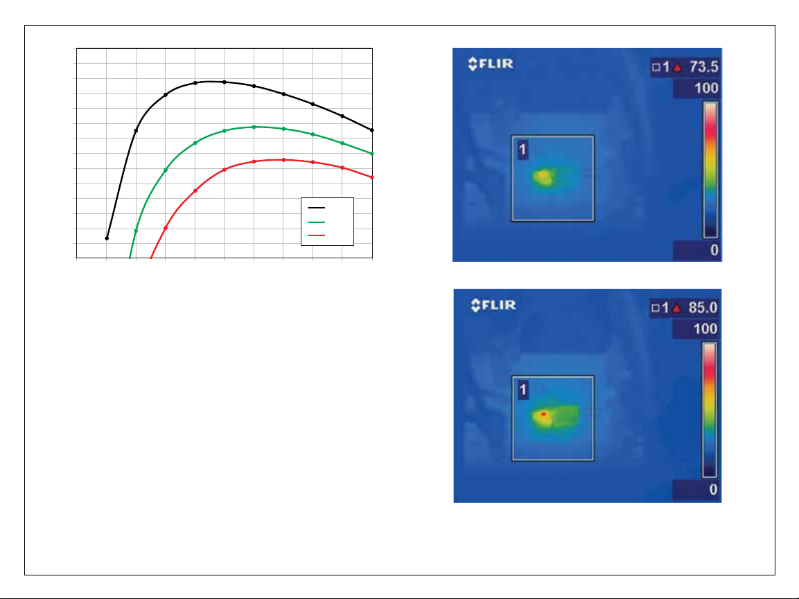
THERMAL CONSIDERATIONS
The EPC9101 demonstration board thermal images for steady
state full load operation are shown in Figure 6. The EPC9101 is
intended for bench evaluation with low ambient temperature
and forced air cooling for higher currents. Care must be taken
to not exceed the absolute maximum die temperature of 125°C
and stay within the constraints of the other components within
the circuit.
NOTE. The EPC9101 demonstration board does not have any current or thermal
protection on board.
Figure 6:Thermal images of EPC9101 under full load conditions
Figure 5:Typical eciency curves for 24 V, 19V and 12 V input including
controller and LDO losses
81
82
83
78
79
80
84
85
86
87
88
89
90
91
92
Eciency
0 2 4 6 8 10 12 18 2014 16
12 VIN
19 VIN
24 VIN
12 VIN, 20 AOUT, 200LFM
24 VIN, 20 AOUT, 200LFM
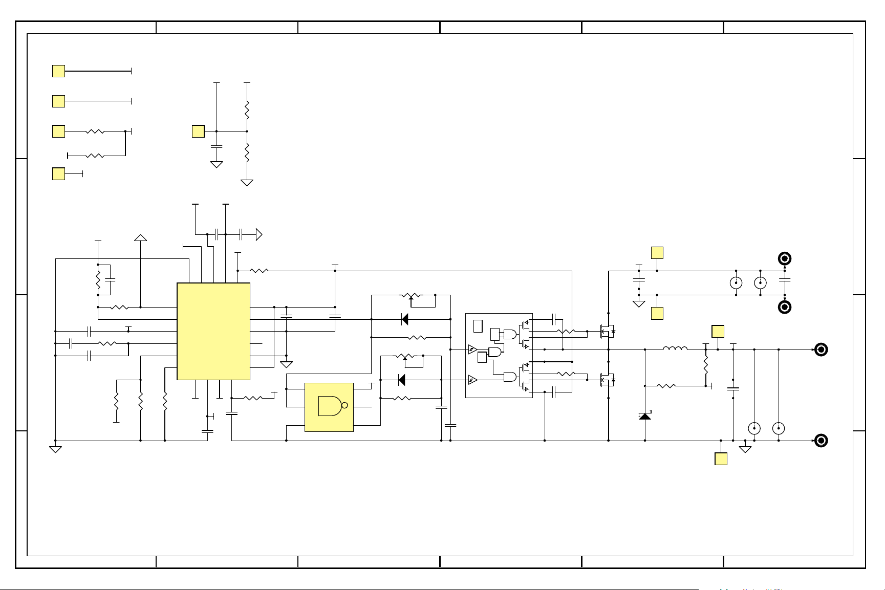
Demonstration Board – EPC9101 Schematic
Rev. 2.0