QUICK START GUIDE EPC90147
EPC – POWER CONVERSION TECHNOLOGY LEADER | EPC-CO.COM | ©2022 | | 4
In no-bypass mode, gure 5(a) (red jumper across pins 5 & 6 of
J640), both the on-board polarity and dead-time circuits are fully
utilized. In dead-time bypass mode, gure 5(b) (red jumpers
across pins 3 & 4 of J640), only the on-board polarity changer
circuit is utilized, eectively bypassing the dead-time circuit.
In full bypass mode, Figure 5(c) (red jumper across pins 1 & 2 of
J640), the inputs to the gate driver are directly connected to the
PWM1 and PWM2 pins and the on-board polarity and dead-time
circuits are not utilized.
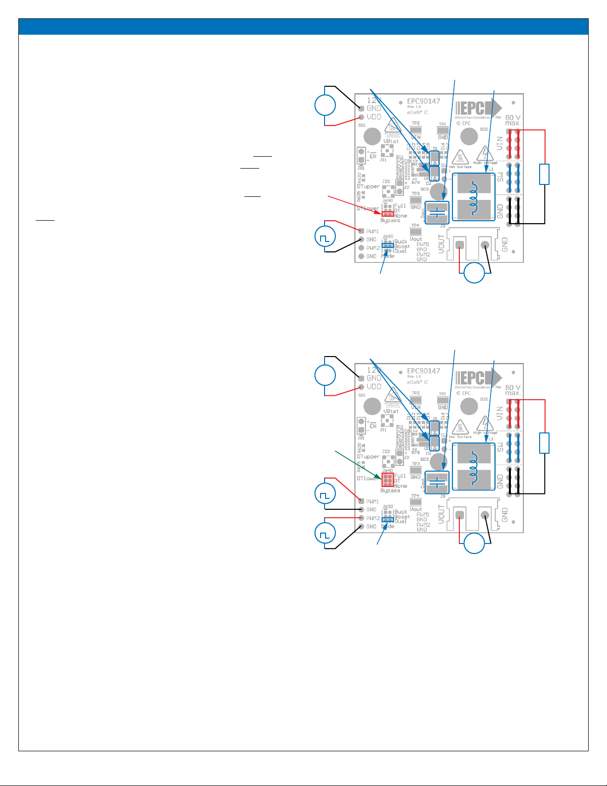
Buck converter conguration
To operate the board as a buck converter, either a single or dual
PWM inputs can be chosen using the appropriate jumper settings
on J630 (mode).
To select Single Input Buck Mode, the bypass jumper J640 must be
set to the no-bypass mode, the buck mode J630 must be selected
as shown in gure 6(a).
To select Dual Input Buck Mode, the bypass jumper J640 may be
congured to any of the valid settings, the dual-input mode J630
must be selected as shown in gure 6(b).
Note: It is important to provide the correct PWM signals that
includes dead-time and polarity when operating in bypass mode.
Once the input source, dead-time settings and bypass cong-
urations have be chosen and set, then the boards can be operated.
1. With power o, connect the input power supply bus to VIN and
ground / return to GND.
2. With power o, connect the switch node (SW) of the half bridge
to your circuit as required (half bridge conguration). Or use the
provided pads for inductor (L1) and output capacitors (Cout), as
shown in gure 6.
3. With power o, connect the gate drive supply to VDD (J1, Pin-1)
and ground return to GND (J1, Pin-2 indicated on the bottom
side of the board).
4. With power o, connect the input PWM control signal to PWM1
and/or PWM2 according to the input mode setting chosen and
ground return to any of GND J2 pins indicated on the bottom
side of the board.
5. Turn on the gate drive supply – make sure the supply is set
between 7.5 V and 12 V.
6. Turn on the controller / PWM input source.
7. Making sure the initial input supply voltage is 0 V, turn on the
power and slowly increase the voltage to the required value
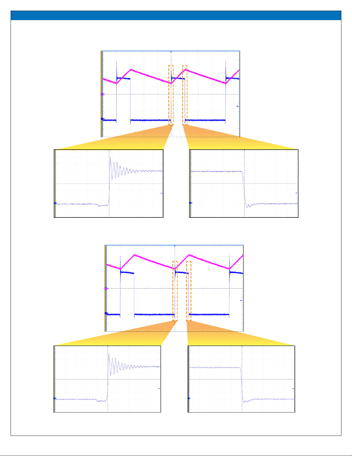
(do not exceed the absolute maximum voltage). Probe switch-
node to see switching operation.
8. Once operational, adjust the PWM control, bus voltage, and load
within the operating range and observe the output switching
behavior, eciency, and other parameters.
9. For shutdown, please follow steps in reverse.
Bypass mode warnings
• It is important to provide the correct PWM signals that includes dead-
time and polarity for either buck or boost operation when making use
of bypass modes.
• When operating in full bypass mode, the input signal specications
revert to that of the EPC23102. Refer to the EPC23102 datasheet for
details.
VDD supply
(Note polarity)
Output Capacitor
Buck Inductor
PWM1
(default)
Jumper positions for
single-input buck
Optional anti-
parallel diodes
DC load
Switch-node
output
Must be in
No-bypass
position
+
+
+
Output Capacitor
Buck Inductor
Optional anti-
parallel diodes
VDD supply
(Note polarity)
VMain
supply
(Note
polarity)
VMain
supply
(Note
polarity)
PWM1
Upper
FET
PWM2
Lower
FET DC load
All valid
positions
permitted
+
+
+
+
Jumper positions for
dual-input buck
12 VDC
80 VDCmax
80 VDCmax
12 VDC
(a)
(b)
Figure 6: (a) Single-PWM input buck converter (b) Dual-PWM input buck converter
congurations showing the supply, anti-parallel diodes, output capacitor,
inductor, PWM, and load connections with corresponding jumper positions.