EPC 9104 User manual

24
Demonstration Board Notication
The EPC9104 board is intended for product evaluation purposes only and is not intended for commercial use. As an evaluation tool, it is not
designed for compliance with the European Union directive on electromagnetic compatibility or any other such directives or regulations. As
board builds are at times subject to product availability, it is possible that boards may contain components or assembly materials that are not
RoHS compliant. Ecient PowerConversionCorporation (EPC)makesno guaranteethat thepurchased boardis100%RoHScompliant. No
Licenses are implied or granted under any patent right or other intellectual property whatsoever. EPC assumes no liability for applications
assistance, customer product design, software performance, or infringement of patents or any other intellectual property rights of any kind.
EPC reserves the right at any time, without notice, to change said circuitry and specications.
EPC Products are distributed exclusively through Digi-Key.
www.digikey.com
Contact us:
www.epc-co.com
Renee Yawger
WW Marketing
Oce: +1.908.475.5702
Mobile: +1.908.619.9678
renee.yawger@epc-co.com
Stephen Tsang
Sales, Asia
Mobile: +852.9408.8351
stephen.tsang@epc-co.com
Bhasy Nair
Global FAE Support
Oce: +1.972.805.8585
Mobile: +1.469.879.2424
bhasy.nair@epc-co.com
Peter Cheng
FAE Support, Asia
Mobile: +886.938.009.706
peter.cheng@epc-co.com
Demonstration Board EPC9104
Quick Start Guide
15 W, 6.78 MHz Class D Wireless Power System
using the EPC2014 eGaN® FET

2
DESCRIPTION
The EPC9104 Wireless power demonstration system is a
class D power system capable of delivering up to 15 W into
a load operating at 6.78 MHz (Lowest ISM band). The purpose
of this demonstration system is to simplify the evaluation pro-
cess of the wireless power technology using eGaN® FETs by in-
cluding all the critical components on a single board that can
be easily connected into any existing converter. The EPC9104
wireless power system comprises four boards namely:
1) A Source Board (Transmitter or Power Amplier)
2) A Source Coil (Transmit Coil)
3) A Device Coil (Receive Coil)
4) A Device Board (Load or Receiver)
The Source board features the EPC2014 (40 V rated) enhance-
ment mode (eGaN®) eld eect transistors (FETs) in a half
bridge topology, and includes the gate driver and feedback
based phase controller that ensures operation of the system
at 6.78 MHz. The source board can also be operated using an
external oscillator or direct gate driver signals.
The Source and Device Coils are provided by WiTricity Corpo-
ration and have been pre-tuned to operate at 6.78 MHz.
The device board includes a high frequency Schottky di-
ode based full bridge rectier and output lter to deliver a
ltered unregulated DC voltage. The device board comes
equipped with various load resistances that can be manually
23
Manufacturer Part #
Murata GRM188R71H104KA93D
Murata GRM32DF51H106ZA01L
Diodes Inc. PD3S140-7
Linx CONREVSMA013.062
Tyco 4-103185-0-02
Stackpole CSRN2512FKR300
----
--
TE Connectivity 5-1622820-3
Rohm Semiconductor MCR100JZHF4220
Rohm Semiconductor MCR100JZHF2740
Rohm Semiconductor MCR100JZHF2870
Rohm Semiconductor MCR100JZHF1400
Tektronix 131-5031-00
Keystone 5015
WiTricity 190-00038-01
Figure 10: EPC9104-D Device Board Schematic
47E Load Bank
CAUTION - HOT
Output
21
R815
274E 1W
GND2
21
R816
274E 1W
GND2
21
R817
287E 1W
GND2
21
R818
287E 1W
GND2
21
R819
287E 1W
GND2
21
R820
287E 1W
GND2
21
R821
140E 1W
GND2
21
R822
140E 1W
GND2
21
R823
140E 1W
GND2
21
GND2
21
GND2
21
GND2
21
GND2
21
GND2
21
GND2
21
GND2
21
GND2
21
GND2
GND2
R803
560E 1W R804
560E 1W R805
560E 1W R806
560E 1W R807
560E 1W R808
560E 1W R809
560E 1W R810
560E 1W R811
560E 1W
J82
.1” Male Vert.
2
1
Vout
J801
.1” Male Vert.
2
1
Vout
J802
.1” Male Vert.
2
1
Vout
J803
.1” Male Vert.
2
1
Vout
J804
.1” Male Vert.
2
1
Vout
J805
.1” Male Vert.
2
1
+Z 137E Load Bank
Load Bank #2
‹
+Z 144E Load Bank
Load Bank #3
‹
+Z 144E Load Bank
Load Bank #4
‹
+Z 140E Load Bank
Load Bank #5
‹
+Z 70E Load Bank
Load Bank #6
‹

22
Table 4 : Bill of Materials - Device Board
Item Qty Reference Part Description
1 1 C84 100nF, 50V
2 1 C85 10uF 50V
34D80,D81,D82,D83 Schottky 40V 1A
4 1 J80 SMA vertical Socket
5 8 J81, J82, J800, J801, J802, J803, J804, J805 .1" Male Vert.
6 1 R80 300mE 1W
7 12 R800, R801, R802, R803, R804, R805, R806,
R807, R808, R809, R810, R811 560E 1W
8 3 R812, R813, R814 422E 1W
9 2 R815, R816 274E 1W
10 4 R817, R818, R819, R820 287E 1W
11 3 R821, R822, R823 140E 1W
12 1 SJ81 5mm Scope Jack
14 4 TP1, TP2, TP3, TP4 SMD probe loop
15 1 Cl2 Device Coil
Board Standos
Output Current - AmpMeter
+Z 140E Load Bank
Load Bank #1
RX Coil Connection
Kelvin Output Current
Kelvin Output Voltage
Receiver Circuit
21
D80
40V 1A
D81
40V 1A C85
10uf, 50V
C84
100nf, 50V
D82
40V 1A
D83
40V 1A
12
R80
300mE 1W
TP4
SMD Probe Loop
J80
SMA
Vertical Socket
TP3
SMD Probe Loop
R800
560E 1W
Vout
Vout
Vrect
Vrect Vrect
GND2
21
R812
422E 1W
GND2
21
R813
422E 1W
GND2
21
R814
422E 1W
GND2
GND2 GND2
GND2
GND2 GND2
21
GND2
21
GND2
R801
560E 1W R802
560E 1W
SJ81
5mm Scope Jack
TP1
SMD Probe Loop
TP2
SMD Probe Loop
J81
.1” Male Vert.
2
1
1
1
J800
.1” Male Vert.
2
1
‹
1
1
www.epc-co.com
3
programmed to specic values to determine the impact of load
resistance on the performance of the system.
Both the source and device boards come equipped with various
probe points to facilitate simple waveform measurement and ef-
ciency calculations. A complete block diagram of the system is
given in Figure 1.
For more information on the EPC2014 eGaN FET please refer to
the datasheet available from EPC at www.epc-co.com. The data-
sheet should be read in conjunction with this quick start guide.
Reverse Engineering of the Source and Device coils is prohibited
and protected by copyright law. For additional information
contact WiTricity Corp. direct or EPC for contact information.
Source Board
Source
Coil
Device
Coil
Un-Regulated
DC Output
Device
Board
Load
WiTricity
Coils
24VDC
+
Matching
Impedance
Network
Matching
Impedance
Network
Feedback and
Basic Control
Gate
Driver
Gate
Driver
PSU
PSU
Figure 1: Block Diagram of EPC9104 Demonstration System

4
ASSEMBLY PROCEDURE
Although the EPC9104 demonstration unit comes mostly pre-
assembled, the standos need to be attached to the system
prior to testing. The standos raise the boards 2 inches above
the work surface to ensure that metal work surfaces do not
interfere with the magnetic elds of the coils. Figure 2 shows
the location and allocation of the standos for the system. It
is recommended to tighten the nuts by hand to prevent over
tightening them.
If the Voltage feedback cable needs to be attached, use cau-
tion when installing as the Source Coil PCB is thin and can eas-
ily break.
When attaching the heat-sink, observe that it lies at (paral-
lel) with respect to the PCB to ensure proper contact to both
FETs and the gate driver IC. Do not over tighten the screws as
this can damage the screws, thermal interface material, and/
or the FETs.
21
Figure 9: EPC9104-S Source Board Schematic
4
4
5
5
6
6
D
C
B
A
Main Coil Supply
2DC - 24VDC
Gate
Driver
High Side Regulator
TX Coil Connection
21
12
R16
0E
U50
5.0V 250mA DFN
U20
LM5113TM
R19
DNP 10k
21
R18
DNP 10k
Hdrv
Ldrv
5VHS
5VHS
Vsup Vsup Vsup
5VHS
GUH
GLH
GLL
GUL
IN
GND
OUT
C14
120pF, 250V
Ldvr
1
1
1
2
R402
0E
12
R405
0E
12
R400
2E2
12
R401
4E7
12
R404
4E7
12
R403
2E2
12
R17
0E
C15
120pF, 250V
SWNode SWNode SWNode SWNode
SWNode
SWNode SWNode
SWNode
Hdvr
5V
5V
C52
100nF, 50V C53
1uF, 25V
C54
1uF, 25V
C40
10uF, 35V C41
10uF, 35V
C20
100nF, 50V Q40
40V 10A 16mohm
EPC2014
Q41
40V 10A 16mohm
EPC2014
J17
SMA Vertical Socket
GU
GL
SJ40
5mm Scope Jack
SJ41
5mm Scope Jack
ProbeHole
SJ42
5mm Scope Jack
C21
4.7uF, 25V
.1” Male Vert.
J44
J46
J62
.1” Male Vert.
Vsup
1
2

20
1
1
2
2
3
3
D
C
B
A
7.5VDC - 12VDC
Direct Gate Drive
TX Coil Voltage Feedback Connection
Control Method
1-2 = Internal Feedback
2-3 = External
Push button to start feedback control
Internal Oscillator
Coil Phase Detect
Gate Signal Generate
Delay Upper
Delay Lower
Board Standos
External
Oscillator Input
Frequency
Adjust
Control Supply Regulator Voltage Reference
J90 Vin
Hdrv
R70
1
1
12
27
8
5
3
4
45
2.5Vref
2.5Vref
3
2
2
2
2
4
6
27
8
5
3
4
6
1
1
21
R71
12
12k
R38
100E
12
R32
DNP 0E
12
R14
150E
R73
12
12k
R74
1 2 VcoilFB
12k
Ldrv
U90
5.0V 250mA DFN U92
2.5V 5mA Ref
Vin 5V 5V
5V
IN
VCC
EN
GND
OUT
OUT
IN
GND
GND
OUT
.1” Male Vert.
.1” Male Vert.
C94
100nF, 50V
J72
SMB Vertical Jack
C30
100nF, 50V
C33
100nF, 50V
D10
40V 30mA
C35
10nF, 50V
R30
10k
R35
4k7
21
R36
4k7
C34
12pF, 50V
1k
R33
C31
47pF, 50V
U30
LT1016CS8#PBF
U31
LT1016CS8#PBF
NegDrv
PosDrv
PosDrv
12
R15
250E
12
R50
1E
D11
40V 30mA
D50
40V 1A
NegDrv
Vin
C78
5V
5V
1
5V
5V
C32
100nF, 50V
5V
5V
C70
10pF 50V
C71
100nF 50V
U70
7.3728MHz CMOS Osc 5V
C90
1uF, 25V C91
1uF, 25V C92
22uF, 25V C93
22uF, 25V
C50
100nF, 50V
J10
1
2
3
2
1
ExtOsc
ExtOsc
IntOsc
IntOsc
ACVcoilFB
ACVcoilFB
ACVcoilFB
100nF, 50V
Coil V
2.5Vref
SW60
SPST push button 42V 0.1A
VcoilFB
.1” Male Vert.
.1” Male Vert.
J61
3
2
1
J60
1
2
www.epc-co.com
5
2 inch standos 3 inch standos
Washer above PCB
Washer below PCB
Figure 2: StandoAssembly for the EPC9104Wireless System

6
The EPC9104 demonstration system is easy to set up and evaluate
the performance of the EPC2014 eGaN FET in a wireless power ap-
plication. Refer to Figure 3 though Figure 6 for proper connection
and measurement setup before follow the testing procedures.
The EPC9104 can be operated using any one of three alternative
methods:
a. Using the built-in phase follower controller.
b. Using an external oscillator.
c. Using direct gating signals.
a. Operation using the built-in phase follower controller
The phase follower controller uses the coil feedback voltage to
generate the gating signals that allow for precise frequency con-
trol, regardless of load. The frequency has been pre-set by EPC to
6.78 MHz.
1. Make sure the entire system is fully assembled prior to making
electrical connections.
2. With power o, connect the main input power supply bus to
+VIN (J62). Note the polarity of the supply connector.
3. With power o, connect the control input power supply bus
to +VDD (J90). Note the polarity of the supply connector.
4. Set the load to the desired value (see table for setting jumpers
or use an appropriate external load).
QUICK START PROCEDURE
19
Manufacturer Part #
TDK C1608C0G2E121J
-----
----- Murata GRM188R71H104KA93D
TDK C1608X5R1C475K
Murata GRM1885C1H470JA01D
Murata GRM1885C1H120JA01D
Murata GRM188R71H103KA93D
Taiyo Yuden GMK325AB7106MM-T
TDK C1608X7R1E105K
Murata GCM1885C1H100JA16D
Kemet C0603C223K3RACTU
Diodes Inc. SDM03U40-7
Diodes Inc. PD3S140-7
Tyco 4-103185-0-03
Tyco 4-103185-0-01
Tyco 4-103185-0-02
Linx CONREVSMA013.062
TE Connectivity 1-1337482-0
EPC EPC2014
Yageo RC0603FR-07150RL
Yageo RC0603JR-07240RL
Stackpole RMCF0603ZT0R00
Yageo RC0603JR-0710KL
Murata PV37Y102C01B00
Yageo RC0603JR-074K7L
Panasonic ERJ-3GEYJ101V
Yageo RC0603FR-071RL
Yageo RC0603JR-0712KL
Yageo RC0402JR-072R2L
Panasonic ERJ-3GEYJ4R7V
Tektronix 131-5031-00
C & K Components 1.14100.5030000 & 5.46167.3010209
Texas Instruments LM5113TM
Linear LT1016CS8#PBF
Microchip MCP1703T-5002E/MC
CTS CB3-3C-7M3728
National LM4125AIM5-2.5
WiTricity 190-00037-01

18
Table 3 : Bill of Materials - Source Board
Item Qty Reference Part Description
1 2 C14, C15 120pF 250V
29
C20, C30, C32, C33, C50, C52, C71,
C78, C94 100nF, 50V
3 1 C21 4.7uF, 25V
4 1 C31 47pF 50V
5 1 C34 12pF, 50V
6 1 C35 10nF, 50V
7 2 C40, C41 10uF 35V
8 4 C53, C54, C90, C91 1uF, 25V
9 1 C70 10pF 50V
10 2 C92, C93 22nF, 25V
11 2 D10, D11 Schottky 40V 30mA
12 1 D50 Schottky 40V 1A
13 2 J10, J61 3pin .1" Male Vert.
14 1 J44 1pin .1" Male Vert.
15 3 J60, J62, J90 2pin .1" Male Vert.
16 1 J71 SMA vertical Socket
17 1 J72 SMB vertical Jack
18 2 Q40, Q41 40V 10A 16mE
19 1 R14 150E
20 1 R15 240E
21 4 R16, R17, R402, R405 0E
22 3 R18, R19, R32 DNP
23 1 R30 10k
24 1 R33 1k
25 2 R35, R36 4k7
26 1 R38 100E
27 1 R50 1E
28 4 R70, R71, R73, R74 12k
29 2 R400, R403 2E2
30 2 R401, R404 4E7
31 3 SJ40, SJ41, SJ42 5mm Scope Jack
33 1 SW60 SPST push button 42V 0.1A
34 1 U20 100V eGaN Driver
35 2 U30, U31 15ns Comparator
36 2 U50, U90 5.0V 250mA DFN
37 1 U70 7.3728MHz CMOS Osc 5V
38 1 U92 2.5V 5mA Ref
39 1 Cl1 Source Coil
www.epc-co.com
7
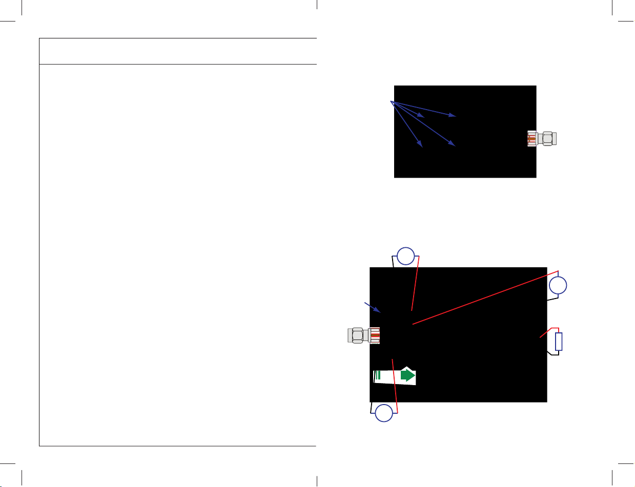
5. Make sure the jumper (J61) is in the internal feedback posi-
tion (default 1-2)
6. Turn on the control supply – make sure the supply is between
7 V and 12 V range (8.5 V is recommended).
7. Turn on the main supply voltage to the required value (do
not exceed the absolute maximum voltage of 24 V on VOUT).
To ensure that the circuit starts, it is recommended to start at
8 V and increase or decrease to the desired value.
8. If the unit does not self-start in step 7, then press the start
button and hold for at least 2 seconds. Observe that the sys-
tem operates on its own once the button has been released.
Pressing the start button will connect the internal oscillator
to the feedback circuit to help establish the currents and
voltages in the system to function on its own upon release
of the start button. The internal oscillator is set to 7.372 MHz
(well above the operating point) and it may be necessary to
increase the voltage or reduce the load to start the circuit.
9. Once operational, adjust the main supply voltage and load
within the operating range and observe the output switch-
ing behavior, eciency and other parameters.
10. For shutdown, please follow steps in the reverse order. Start
by reducing the main supply voltage to 0 V followed by steps
6 through 2.

8
7 V – 12 VDC
3 V – 24 VDC
Lower FET Gate Oscilloscope
Lower FET
Upper FET
External
Gate Signal
(Operation
conly)
External
Oscillator
(Operation
bonly)
Upper FET Gate
Oscillatoscope Probe
Switch-node
Oscilloscope Probe
Switch-node -
hole & post
(see Notes
for details)
VIN Supply
(note polarity)
Source Coil
Connection
Coil Voltage
Feedback
(Operation
aonly)
Gate Drive and
Control Supply
(note polarity)
EPC
EFFICIENT POWER CONVERSION
+
+
Figure 3: Proper Connection and Measurement Setup for the Source Board
Figure 4: Proper Connection and Measurement Setup for the Source Coil
Mechanically
Attached
Device Coil
to these
locations
Source
Board
Connection
Coil
Voltage
Feedback
(see Notes
for details)
www.epc-co.com
17
• Avoid contact with the load bank surface as it can be hot when in operation.
• Never operate the system without a load or a load less than the minimum
built into the Device board as this can cause currents in the source circuit to
become very high and lead to over-current failure.
• Always make use the ammeter is connected to the load circuit when NOT
using the built-in load current shunt. An open circuit can cause currents in
the source circuit to become very high and lead to over-current and/ or over-
voltage failure.
• Do not change load jumper settings when circuit is in operation.
• Do not press the start button after the system has started and is operating on
its own when using the coil voltage feedback method.
• Never press the start button when using an external oscillator for control.
• Never disconnect any of the coils while the circuit is in operation.
• When attempting tests with multiple device loads, always make sure at least
one device load is correctly set and physically in proximity to the source coil
such that the system operates within specications.
• When conducting tests near or at full power, always monitor the temperature
of the heat-sink and matching circuit inductors to ensure that operation is
within specications.
• Never attempt to monitor, using standard oscilloscope probes, the upper gate
voltage (SJ40) simultaneously with the lower gate voltage (SJ42) with any volt-
age applied to the main circuit (J62). The oscilloscope probes will short out the
lower device and induce the possibility of a shoot-through condition for the
upper device which can lead to failure. The only exception is if the upper gate
voltage is being monitored using an approved dierential probe, however
even this method of measurement must be limited as induced stray capaci-
tances and inductances can signicantly alter the performance of the circuit
and resulting oscillations may lead to over-voltages and ultimately failure.
• Always use the supplied hardware to re-assembly the unit and never substi-
tute metal screws, nuts and washers for the nylon versions as they may induce
short-circuits into the boards.

16
The EPC9104 demonstration system showcases the EPC2014 eGaN
FET in a wireless application. Although the electrical performance
surpasses that for traditional Si devices, their relatively smaller
size does magnify the thermal management requirements. The
EPC9104 is intended for bench evaluation with low ambient tem-
perature and convection cooling with load power up to 10 W (the
heat-sink MUST be mounted to the board). The addition of forced
air cooling can signicantly increase the power output of this sys-
tem, but care must be taken to not exceed the absolute maximum
die temperature of 125°C.
NOTE. The EPC9104 demonstration system does not have any current or thermal
protection on board. The source coil matching inductor will also dissipate signi-
cant power at load power > 10 W and care must be taken to force air cool this induc-
tor too during operation.
GENERAL PRECAUTIONS
• Do not operate the board without a heat-sink as the FETs will overheat and fail.
• Avoid contact with the coil feedback voltage as it can be as high as 300 Vpeak.
• Do not operate the system below resonance as the load will appear capaci-
tive and the losses in the FETs will become very high and lead to thermal
failure. When testing the system at various frequencies, always start higher
than 6.78 MHz and slowly reduce the frequency, whilst monitoring the source
coil current, until the desired setting or the peak amplitude has been reached
(resonant point). Operating below this frequency is considered below resonance.
• Do not operate the system on a solid metal (or conductive) surface without
the standos provided as this will shunt the magnetic eld and lead to over-
current of the FETs.
• Do not apply magnetic materials to the coil magnetic elds as this will shift the
resonant operating points and can lead to failure.
THERMAL CONSIDERATIONS
9
Figure 5: Proper Connection and Measurement Setup for the Device Coil
Figure 6: Proper Connection and Measurement Setup for the Device Board
Mechanically
Attached
Source Coil
to these
locations
Device
Board
Connection
EPC
EFFICIENT POWER CONVERSION
Device Coil
Output
Voltage
(see Notes
for details)
Load
Current
(see Notes
for details)
*ONLY to be
used with
Shunt
removed
External
Load
(see Notes
for details)
Device Coil
Connection
mV
A
V

10
b. Operation using an external oscillator
Using an external oscillator allows the user to specify an operating
frequency. The external oscillator voltage may be pure AC (sine or
square wave) or have a DC oset (seeTable 1 for voltage limits).
1. Prior to commencing with testing, jumper (J61) will need to
be moved from its 1-2 position (default) to position 2-3.
2. Using this method, it is not necessary to connect the source
coil feedback voltage RF cable between the source coil and
the source board
3. Make sure the entire system is fully assembled prior to making
electrical connections.
4. With power o, connect the main input power supply bus to
+VIN (J62). Note the polarity of the supply connector.
5. With power o, connect the control input power supply bus
to +VDD (J90). Note the polarity of the supply connector.
6. Set the load to the desired value (see table for setting jumpers
or use an appropriate external load).
7. Turn on the control supply – make sure the supply is between
7 V and 12 V range (8.5 V is recommended).
8. Turn on the main supply voltage starting at 0 V and increase
slowly to the required value (do not exceed the absolute
maximum voltage of 24 V on V
OUT). Observe that the system
operates.
QUICK START PROCEDURE www.epc-co.com
15
EPC
EFFICIENT POWER CONVERSION
Do not use
probe ground
lead
Place probe tip
in large via
Minimize loop
Ground probe
against post
* Can only be used if heat-sink has been removed and post has been installed
Figure 7: Proper Measurement of Switch Node using the hole and post
Figure 8: Typical Waveforms for VIN = 24 V (6.639 MHz) into 23 Ωload
CH1: (VOUT) Device Coil OutputVoltage – CH2: (VGS_L) Lower FET Gate Voltage
CH3: (VOUT) Switch node voltage – CH4: (IOUT) Source Coil Current
Device
Coil
Output
Switch-
Node
0
Source
Coil
Input
Current
Lower
Gate
0
0
0
t
-
e
e
l
t
t
r
r
e
0
0
0
e
l
t

14
The device board comes pre-equipped with various loads that can
be manually programmed to specic values. Table 2 provides a list
of all possible combinations to set the load. This list is the recom-
mended list and it can be recognized that there are a total of 64
combinations, of which many load values will repeat.
LOAD SETTINGS
Table 2 : Device Board Load Resistance Jumper Settings
Setting J800 J801 J802 J803 J804 J805 Load
Resistance [Ω]
1 out out out out out out 47.0
2 out out in out out out 35.5
3 in out out out out out 35.3
4 out in out out out out 35.1
5 out out in in out out 28.6
6 in out in out out out 28.5
7 out out in out in out 28.4
8 in out out out in out 28.3
9 in in out out out out 28.2
10 in out in in out out 23.8
11 in in out in out out 23.7
12 in in out out in out 23.6
13 out in out out out in 23.5
14 in out in in in out 20.5
15 in in in in out out 20.4
16 in in in out in out 20.3
17 out in out out in in 20.2
18 in in in in in out 17.9
19 in in out out in in 17.8
20 in in out in in in 15.9
21 in in in in in in 14.3
www.epc-co.com
11
9. Once operational, adjust the main supply voltage and oscil-
lator frequency within the operating range and observe the
output switching behavior, eciency and other parameters.
10. For shutdown, please follow steps in the reverse order. Start by
reducing the main supply voltage to 0 V followed by steps 7
through 4.
Table 1 : Performance Summary (TA = 25 °C)
Symbol Paramter Conditions Min Max Units
VDD Control Supply Input Range 7 12 V
VIN Bus Input Voltage Range 3 24 V
VOUT Switch Node Output Voltage 40 V
IOUT Switch Node Output Current 10* A
Vextosc # External Oscillator
input threshold Input ‘High’ 0 5 V
Input ‘Low’ -5 0 V
VHIN, VLIN Gating Signal Voltage Range -0.3 15 V
Vfdbk Coil feedback voltage input 300pk V
* Assumes inductive load, maximum current depends on die temperature –
actual maximum current with be subject to switching frequency, bus voltage
and thermals.
# Accepts AC signals with peak magnitude up to 10 V and with DC oset up to 5VDC.

12
c. Operation using direct gating signal control
This method of operating the wireless system is similar to opera-
tion using an external oscillator except the user now directly con-
trols the gating signals. It is important to note that the user MUST
provide the necessary dead-time between the high side (29 ns
recommended) and low side (18 ns recommended) signals and
also ensure that both gating signals cannot be high at the same
time as these features have not been built into the circuit when
sourcing the gating signals directly. This has been an intentional
omission allowing users to integrate their custom circuits to as
close to their needs as possible.With this method the entire phase
follower feedback circuit is bypassed.
1. Prior to connecting the source board to the source coil, resis-
tors R16 (0 Ω, size 0603) and R17 (0 Ω, size 0603) must be re-
moved from the board. Resistors R18 (10 kΩ, size 0603) and
R19 (10 kΩ, size 0603) must be inserted.
2. Using this method, it is not necessary to connect the source
coil feedback voltage RF cable between the source coil and
the source board.
3. Make sure the entire system is fully assembled prior to making
electrical connections.
4. With power o, connect the main input power supply bus to
+VIN (J62). Note the polarity of the supply connector.
5. With power o, connect the gate drive input signals to (J10,
Pin-1 = Low-side, Pin-2=Ground, Pin-3=High-side) and activate
signals. Make sure the gating signal are within specications.
QUICK START PROCEDURE www.epc-co.com
13
6. With power o, connect the control input power supply bus
to +VDD (J90). Note the polarity of the supply connector.
7. Set the load to the desired value (see table for setting jump-
ers or use an appropriate external load).
8. Turn on the control supply – make sure the supply is between
7 V and 12 V range (8.5 V is recommended).
9. Turn on the main supply voltage starting at 0 V and increase
slowly to the required value (do not exceed the absolute
maximum voltage of 24 V on V
OUT). Observe that the system
operates.
10. Once operational, adjust the main supply voltage and oscil-
lator frequency within the operating range and observe the
output switching behavior, eciency and other parameters.
11. For shutdown, please follow steps in the reverse order. Start
by reducing the main supply voltage to 0 V followed by steps
8 through 4.
NOTE. When measuring the high frequency content switch-node (Source Coil
Voltage), care must be taken to avoid long ground leads. An oscilloscope probe
connection (preferred method) has been built into the board to simplify the mea-
surement of the Source Coil Voltage (SJ41) and the Device Coil Voltage (SJ81) that
is compatible with 5 mm Tektronix probes.
Alternatively, by removing the heat-sink, the Source Coil Voltage can be mea-
sured by placing the oscilloscope probe tip through the large via on the switch-
node (J46 - designed for this purpose) and grounding the probe directly across
the GND post (J44 - must be installed). See Figure 7 for proper scope probe tech-
nique. Using this technique will signicantly limit the operating power as the FETs
and gate driver IC will heat up signicantly and care must be taken not to exceed
the junction temperature of the eGaN FETs.
Table of contents
Other EPC Motherboard manuals
Popular Motherboard manuals by other brands

Aaeon
Aaeon PCM-6890 user manual

Texas Instruments
Texas Instruments ADC12J4000EVM user guide

Silicon Laboratories
Silicon Laboratories Si5338 user guide

Meerstetter Engineering
Meerstetter Engineering LTC-1141 user manual

Linear Technology
Linear Technology DC1765A Demo Manual

VIA Technologies
VIA Technologies P4X266-PE11-L user manual