EPC EPC9084 User manual

Development Board
EPC9084
Quick Start Guide
350 V Half-Bridge with Gate Drive, Using EPC2050
Revision 1.0

2 | | EPC – EFFICIENT POWER CONVERSION CORPORATION | WWW.EPC-CO.COM | COPYRIGHT 2018
QUICK START GUIDE EPC9084
DESCRIPTION
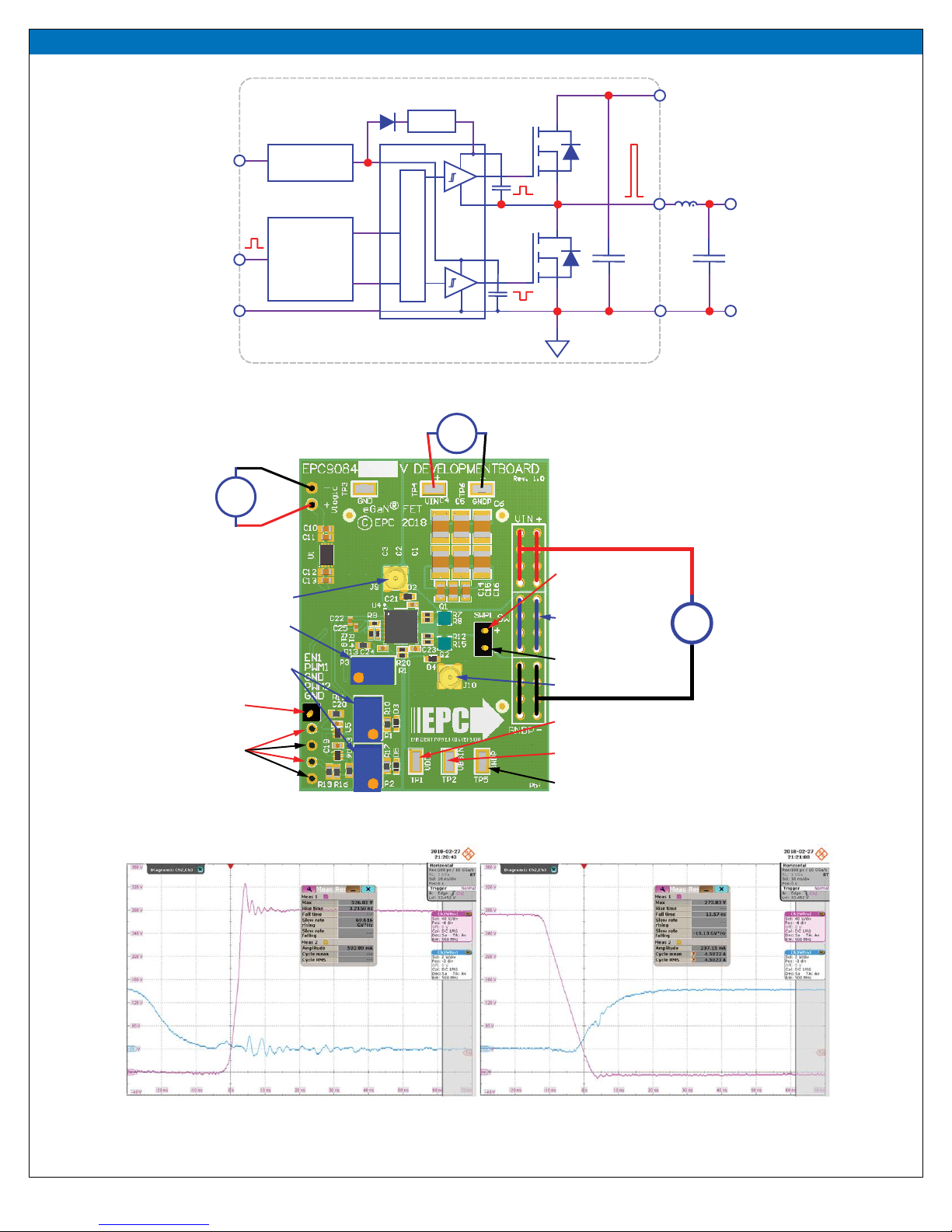
The EPC9084 development board, gure 1, is a 350 V maximum device
voltage, 4 A maximum output current, half bridge with onboard gate
drives, featuring two EPC2050 enhancement mode (eGaN®) eld eect
transistors (FETs). The purpose of this development board is to simplify
the evaluation process of the EPC2050 eGaN FETs by including all the
critical components on a single board that can be easily connected into
any existing converter.
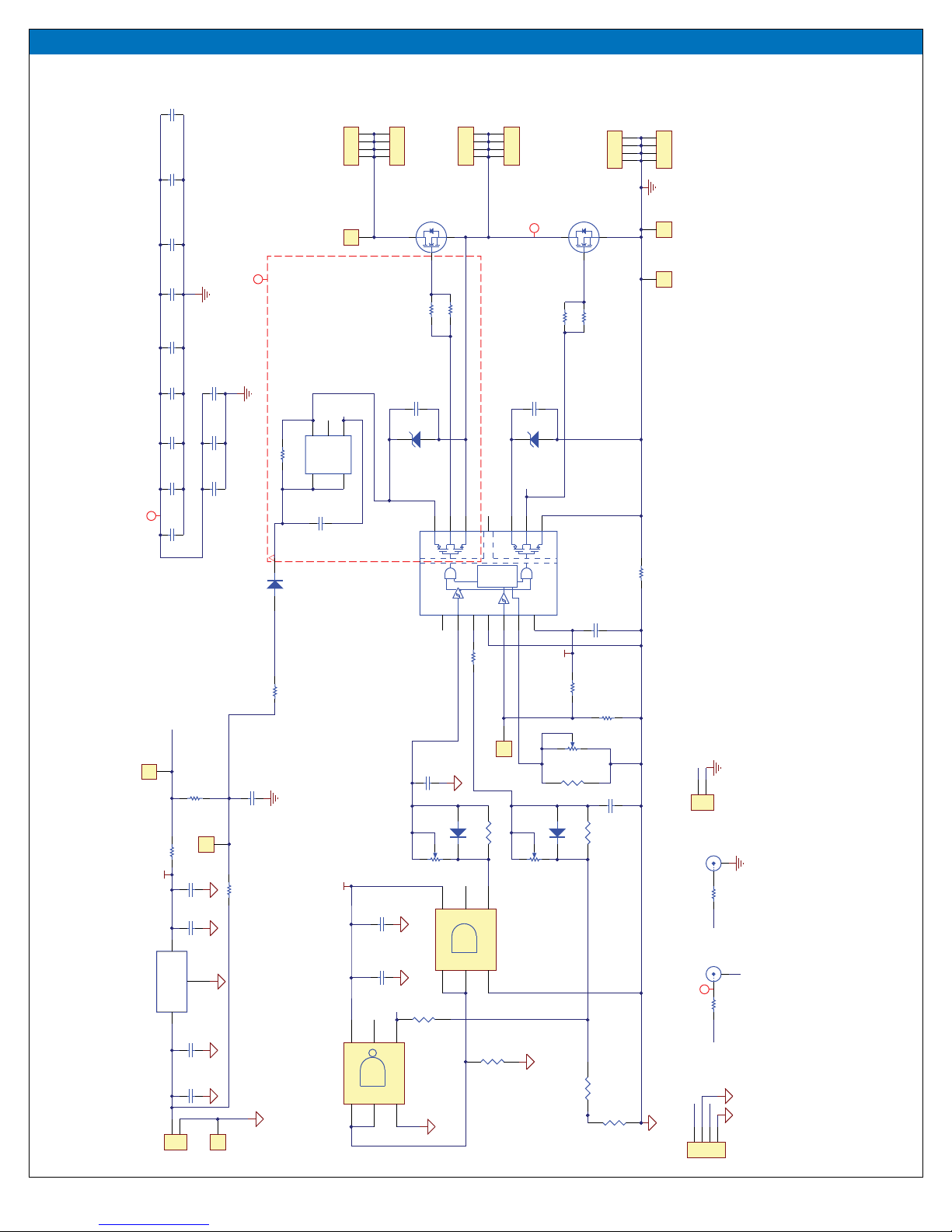
The EPC9084 development board is 1.5” x 2” and contains two
EPC2050 eGaN FETs in a half bridge conguration. As supplied, the
high side gate drive uses a digital isolator and both FETs use the
Silicon Labs SI8274GB1-IM gate driver. The board also contains all
critical components and layout for optimal switching performance.
There are also various probe points to facilitate simple waveform
measurement and eciency calculation, as well as the option to add
trimmer resistors for adjustable deadtime to provide separate high
and low side inputs, and an isolator for the low side gate drive. A block
diagram of the circuit is given in gure 2.
For more information on the EPC2050 please refer to the datasheet
available from EPC at www.epc-co.com. The datasheet should be
read in conjunction with this quick start guide.
QUICK START PROCEDURE
Development board EPC9084 is easy to set up to evaluate the
performance of EPC2050 eGaN FETs. Refer to gure 3 for proper connect
and measurement setup and follow the procedure below:
1. With power o, connect the input power supply bus to +VIN (J5, J6) and
ground / return to –VIN (J7, J8).
2. With power o, connect the switch node (SW) of the half bridge OUT
(J3, J4) to your circuit as required (half bridge conguration).
3. With power o, connect the gate drive power supply to +VDD
(J1, Pin-1) and ground return to –VDD (J1, Pin-2).
4. With power o, connect the input PWM control signal to PWM
(J2, Pin-1) and ground return to any of the remaining J2 pins.
5. Turn on the gate drive supply – make sure the supply is between 7.5 V
and 12 V range.
6. Turn on the controller / PWM input source.
7. Turn on the bus voltage to the required value (do not exceed the
absolute maximum voltage) and probe switching node to see
switching operation.
8. Once operational, adjust the PWM control, bus voltage, and load within
the operating range and observe the output switching behavior,
eciency and other parameters.
9. For shutdown, please follow steps in reverse.
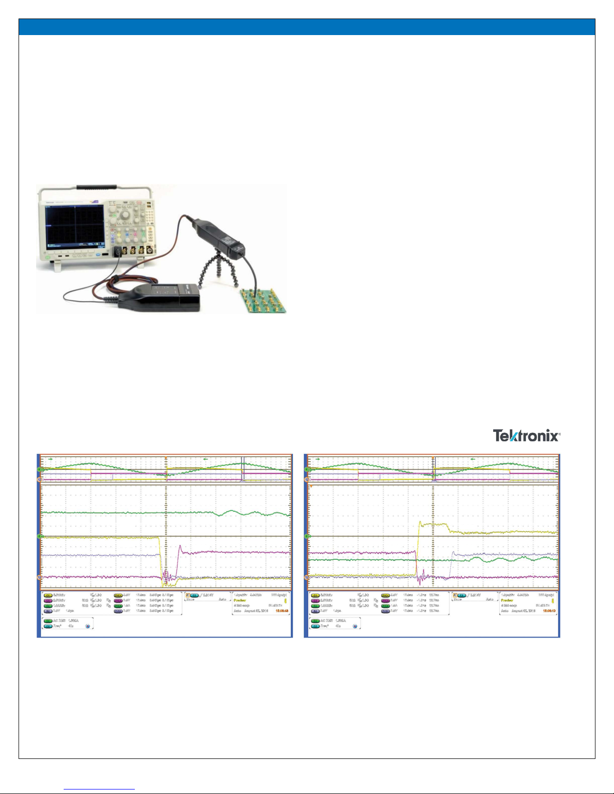
NOTE. When measuring the high frequency content switch node, care
must be taken to provide an accurate high speed measurement. An
optional two pin header (SWP1) is included for switch node measurement.
It is recommended to install measurement point on backside of board to
prevent contamination of the top side components.
For information about measurement techniques, please review the how
to GaN series: HTG09- Measurement
http://epc-co.com/epc/DesignSupport/TrainingVideos/HowtoGaN/
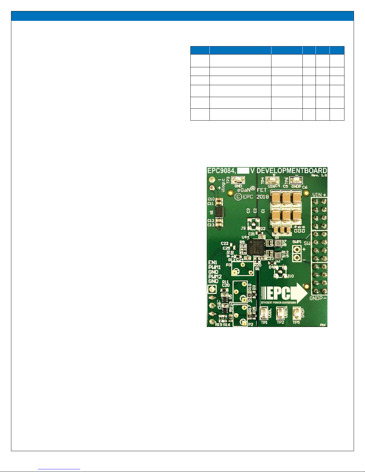
Figure 1: EPC9084 development board
Table 1: Performance Summary (TA= 25°C) EPC9084
Symbol Parameter Conditions Min Max Units
VDD Gate Drive Input Supply Range 7.5 12 V
VIN Bus Input Voltage Range(1) 280 V
IOUT Switch Node Output Current (2) 4 A
VPWM
PWM Logic Input Voltage
Threshold
Input ‘High’
Input ‘Low’
3.5
0
6
1.5
V
V
Minimum ‘High’ State
Input Pulse Width
VPWM rise and
fall time < 10ns 200 ns
Minimum ‘Low’ State Input
Pulse Width (3) VPWM rise and
fall time < 10ns 500 ns
(1) Maximum input voltage depends on inductive loading, maximum switch node ringing must be kept
under 350 V for EPC2050.
(2) Maximum current depends on die temperature – actual maximum current with be subject to
switching frequency, bus voltage and thermal cooling.
(3) Limited by time needed to ‘refresh’ high side bootstrap supply voltage.

QUICK START GUIDE EPC9084
EPC – EFFICIENT POWER CONVERSION CORPORATION | WWW.EPC-CO.COM | COPYRIGHT 2018 | | 3
VIN = 280, VOUT = 28 V, IOUT = 4 A, fSW = 50 kHz, LBuck = 440 μH
VDS = 40 V/div
VGSQ2 = 2 V/div
10 ns/div
Figure 3: Proper connection and measurement setup
Figure 4: TypicalWaveform for the EPC9084 operating as a buck converter
Figure 2: Block diagram of EPC9084 development board
CBypass COUT
LBuck
Isolation
PGND
Gate drive
regulator
Logic and
dead-time
adjust
VDD
VIN
Q1
Q2
GND
PWM
Output
DC Output
Gate driver (Si8274)
LDO
EPC9084
7.5 – 12 VDC
280 VDCmax
Main Voltage Measurement
(HIGH VOLTAGE)
Switch-node
oscilloscope probe
Ground
oscilloscope probe
Output
G2 Gate
5 V control supply voltage
DC Control supply Voltage
Ground
VIN supply
(note polarity)
VMain supply
(note polarity)
Q1 Gate
(HIGH VOLTAGE!)
Dead-time Adjust
(Single PWM)
Dead-time Adjust
(Dual PWM)
Enable
Control
Signal
Inputs
+
+
>

QUICK START GUIDE EPC9084
EPC – EFFICIENT POWER CONVERSION CORPORATION | WWW.EPC-CO.COM | COPYRIGHT 2018 | | 4
MEASUREMENT CONSIDERATIONS
The EPC9084 development board has been provided with
specially designed high frequency (up to 1 GHz minimum) capable
measurement connections using MMCX connectors located at J9 & J10
with direct access to the gate signals of both the upper and lower FETs.
These nodes can be measured directly using the Tektronix IsoVu probe
shown in gure 4. Figure 5 shows typical gate waveforms measured
using the IsoVu probe.
Figure 4:Tektronix IsoVu measurement setup
This native connection between the high and low side gate-source nodes
to an IsoVu probe tip cable has less than 2 pF common mode loading
and completely eliminates ground loops due to its galvanic isolation.
These MMCX connectors (option not installed) oer a shielded coaxial
environment to the test point which minimizes noise pickup.
Please contact EPC for special instructions on using these connections.
To prevent an unterminated transmission line hanging on the gate it
is recommended to remove resistors R21 & R22 when not using this
feature. The maximum impedance loading of these nodes is 2.5 kΩ.
Tektronix is a leading manufacturer of power test solutions for design
validation, characterization, and performance testing. EPC partnered
with Tektronix to dene the requirements for accurate measurements
on GaN devices which led to the development of the Tektronix IsoVu
measurement system. IsoVu is a galvanically isolated dierential
measurement system with 1 GHz bandwidth, 1 Million to 1 (120 dB)
common mode rejection ratio, 50 V dierential, and 2000 V common
mode voltage range. Previously impossible dierential measurements
such as the high-side VGS are now possible because of IsoVu’s high
common mode rejection across bandwidth.
IsoVu allows you to:
• Characterize the time alignment of high side and low side events
• Optimize and tune switching characteristics such as edge rates,
overshoot, ringing and dead time
• See the interactions due to parasitic coupling between the high and
low side transistors
• Make isolated high frequency current measurements using low
impedance sense resistors
• Improve reliability through accurate characterization across all
operating conditions
EPC would like to acknowledge Tektronix (http://www.tek.com/isolated-
measurement-systems) for their support of this project.
VSW VSW
GHS GHS
GLS GLS
Figure 5: Upper gate and lower gate measurements using theTektronix IsoVu and
switch-node voltage measurement using theTPP1000 probe

5 | | EPC – EFFICIENT POWER CONVERSION CORPORATION | WWW.EPC-CO.COM | COPYRIGHT 2018
QUICK START GUIDE EPC9084
THERMAL CONSIDERATIONS
The EPC9084 development board showcases the EPC2050 eGaN FET.The
EPC9084 is intended for bench evaluation with typical room ambient
temperature. The addition of heat-sinking and forced air cooling can
signicantly increase the current capability of these devices, but care
must be taken to not exceed the absolute maximum die temperature
of 150° C.
NOTE. The EPC9084 development board does not have any current or
thermal protection on board.
For more information regarding the thermal performance of EPC eGaN FETs,
please consult:
D. Reusch and J. Glaser, DC-DC Converter Handbook, a supplement to GaN
Transistors for Ecient Power Conversion, First Edition, Power Conversion
Publications, 2015.
Table 2: Bill of Materials
Item Qty Reference Part Description Manufacturer / Part #
1 4 C11, C12, C13, C17
Capacitor, 1 μF, 50 V
Taiyo Yuden UMK107AB7105KA-T
2 1 C10
Capacitor, 4.7 μF, 25 V
TDK C1608X5R1E475K080AC
3 2 C22, C25
Capacitor, 100 pF, 50 V
TDK CGA2B2C0G1H101J050BA
4 3 C14, C15, C16
Capacitor, 10 nF, 630 V
TDK C0805W103KBRAC7800
5 3 C18, C21, C23
Capacitor, 0.47 μF, 25 V
TDK C1005X5R1E474K050BB
6 3 C19, C20, C24
Capacitor, 0.22 μF, 16 V
TDK C1005X7R1C224K050BC
7 9 C1, C2, C3, C4, C5, C6, C7, C8, C9
Capacitor, 0.1 μF, 630 V
TDK CGA6L1X7T2J104K160AE
8 1 J1
Connector, .1" Male Vert.
Würth 61300211121
9 1 J7
Connector, .1" Male Vert.
Tyco 4-103185-0-04
10 2 TP1, TP2
SMD probe loop
Keystone 5015
11 4 TP3, TP4, TP5, TP6
SMD probe loop
Keystone 5015
12 2 D2, D4
Zener Diode, 5.61 V
On Semiconductor MM5Z5V6ST1G
13 2 D3, D5
Schottky Diode, 30 V, 30 mA
Diodes Inc. SDM03U40-7
14 2 Q1, Q2
eGaN FET, 350 V 4 A 150 mΩ
EPC EPC2050
15 5 R1, R3, R4, R14, R20
Resistor, 0 Ω
Panasonic ERJ-2GE0R00X
16 4 R7, R8, R12, R15
Resistor, 10 Ω
Panasonic ERJ-2RKF10R0X
17 1 U1
IC, 5.0 V 250mA DFN
Microchip MCP1703T-5002E/MC
18 1 U2
IC, 5 V 80 mA
Microchip MIC5213-5.0YC5
19 1 U3
IC, 2 In NAND
Fairchild NC7SZ00L6X
20 1 U5
IC, 2 In AND Fairchild NC7SZ08L6X
21 1 R10
Resistor, 0 Ω Stackpole ERJ-2GE0R00X
22 1 R11
Resistor, 10 k, 1% Stackpole RMCF0603FT10K0
23 1 R13
Resistor, 8.2 k, 1% Panasonic ERJ-3EKF8201V
24 1 R17
Resistor, 470 Ω, 1% Stackpole RMCF0603FT470R
25 1 R6
Resistor, 0 Ω
Panasonic ERJ-3GEY0R00V
26 1 D1
Diode, 600 V 200 mA
ROHM RFU02VSM6STR
27 1 U4
DGTL ISO 2.5KV GATE DRIVE
Silicon Labs Si8274GB1-IM
Table 3: Optional Components
Item Qty Reference Part Description Manufacturer / Part #
1 1 EN1
Connector, .1" Male Vert.
Würth, 61300111121
2 3 FD1, FD2, FD3
Sml Fiducial
N/A
3 6 J2, J3, J4, J5, J6, J8
Connector
N/A
4 2 J9, J10
MMCX SMD
Molex, 0734152063
5 4 R2, R5, R9, R18
Resistor, 0 Ω
Panasonic, ERJ-2GE0R00X
6 2 R16, R19
Optional 0603 Resistor
N/A
7 2 R21, R22
Resistor, 0 Ω
Stackpole, RMCF0402ZT0R00
8 3 P1, P2, P3
Optional Potentiometer
N/A
9 1 SWP1
Connector, .1" Male Vert.
Würth, 61300111121

QUICK START GUIDE EPC9084
EPC – EFFICIENT POWER CONVERSION CORPORATION | WWW.EPC-CO.COM | COPYRIGHT 2018 | | 6
Figure 5: EPC9084 - Schematic
0.47 μF, 25 V
C21
1
2
3
4
J8
CON4
1
2
3
4
J6 CON4
1
2
3
4
J4
CON4
1
2
3
4
J5
CON4
1
2
3
4
J3
CON4
1
2
3
4
J2
CON4
1
TP4
Keystone 5015
1
TP6
Keystone 5015
10 k, 1%
R11
GND
3
A
1
B
2
Y4
VDD 6
55
U3
NC7SZ00L6X
0 Ω
R6
R16
EMPTY
R19
EMPTY
470 Ω, 1%
R17
30 V, 30 mA
D5
0
R10
GND
3
A
1
B
2
Y4
VDD 6
5
U5
NC7SZ08L6X
10 nF, 630 V
C15
10 nF, 630 V
C14
GDH
GDL
VIN
VSW
DRL
DRH
PWM1
GND
PWM2 DL
DH
DZH
0.1 μF, 630 V
C1
0.1 μF, 630 V
C2
0.1 μF, 630 V
C3
0.1 μF, 630 V
C4
0.1 μF, 630 V
C5
VIN
0.1 μF, 630 V
C6
1
2
3
4
.1" Male Vert
.
J7
PWM1
GND
GND
PWM2
.1" Male Vert
.
1
2
J1
.1" Male Vert.
1
2
SWP1
EMPTY
Switch Node SIP Probe
VSWMMCX SMD
J9
EMPTY
MMCX SMD
J10
EMPTY
0 Ω
12 R21
EMPTY
0 Ω
12 R22
EMPTY
MMCX Gate Probes
GDH GDL
VSW
10 nF, 630 V
C16
D2
MM5Z5V6ST1G
D4
MM5Z5V6ST1G
DNP 1k
P1
DNP 1k
P2
i
Net Class
ClassName: HighVoltageGate
i
Net Class
ClassName: HighVoltage
i
Net Class
ClassName: HighVoltageGate
7.5 VDC - 12 VDC
MCP1703T-5002E/MC
5.0 V 250 mA DFN
OUT
GND
IN
GND
U1
Logic Suppl
y
1 uF, 50 V
C11
1 uF, 50 V
C12
1 uF, 50 V
C13
0
12
R2
EMPTY
4.7 uF, 25 V
C10
5V
0.22 μF, 16 V
C24
0.47 μF, 25 V
C23
5V
5V
1
.1" Male Vert.
EN1 DNP
8.2k, 1%
R13
0
1 2
R14
0
12
R18
EMPTY
0
1 2
R9
EMPTY
10
12
R7
10
1 2
R8
10
1 2
R12
10
1 2
R15
600V 200mA
D1
0
1 2
R4
0
1 2
R1
0.22 μF, 16 V
C19
0.22 μF, 16 V
C20
1
5 4
3
2
GND
OUT
NC
EN
IN
LDO
U2
MIC5213-5.0YC5
0
1 2
R3
VSW
0
1 2
R5
EMPTY
0.47 μF, 25 V
C18
VDDH
VDDL
VDDH
VDDL
0
1 2
R20
VBSIN
1
TP5
Keystone 5015
30 V, 30m A
D3
1
TP2
5015
1
TP3
Keystone 5015
1
TP1
5015
100 pF, 50 V
C22
100 pF, 50 V
C25
GNDP
GNDP
GNDP
GNDP
GNDP
i Net Class
ClassName: HighVoltageGate
GLO
6
4
1
5
VDDA
GNDA
VOA
EN
PWM
2
3
GNDI
8
14
12
9
13
10
11
NC
NC
VDDI
VDDB
GNDB
VOB
NC
7
DT
DT
Logic
U4
Si8274GB1-IM
DNP 100k
P3
0.1 μF, 630 V
C7
0.1 μF, 630 V
C8
0.1 μF, 630 V
C9
1 uF, 50 V
C17
GNDP
300 V 4A 150 mΩ
Q1
EPC2050
300 V 4A 150 mΩ
Q2
EPC2050

Demonstration Board Notication
The EPC9084 board is intended for product evaluation purposes only and is not intended for commercial use. Replace components on the Evaluation Board only with those parts shown on
the parts list (or Bill of Materials) in the Quick Start Guide. Contact an authorized EPC representative with any questions.
This board is intended to be used by certied professionals, in a lab environment, following proper safety procedures. Use at your own risk.
As an evaluation tool, this board is not designed for compliance with the European Union directive on electromagnetic compatibility or any other such directives or regulations. As board
buildsareattimes subjectto product availability,it is possiblethatboardsmaycontaincomponentsorassemblymaterialsthatarenotRoHScompliant.EcientPower Conversion Corpora-
tion (EPC) makes no guarantee that the purchased board is 100% RoHS compliant.
The Evaluation board (or kit) is for demonstration purposes only and neither the Board nor this Quick Start Guide constitute a sales contract or create any kind of warranty, whether express
or implied, as to the applications or products involved.
Disclaimer: EPC reserves therightatany time, without notice, to makechanges to any products described hereintoimprove reliability, function, or design.EPC doesnot assumeanyliability
arising out of the application or use of any product or circuit described herein; neither does it convey any license under its patent rights, or other intellectual property whatsoever, nor the
rights of others.
EPC Products are distributed through Digi-Key.
www.digikey.com
For More Information:
or your local sales representative
Visit our website:
www.epc-co.com
Sign-up to receive
EPC updates at
bit.ly/EPCupdates
or text“EPC”to 22828
Table of contents
Other EPC Motherboard manuals