QUICK START GUIDE
EPC – EFFICIENT POWER CONVERSION CORPORATION | WWW.EPC-CO.COM | COPYRIGHT 2015 | | PAGE 5
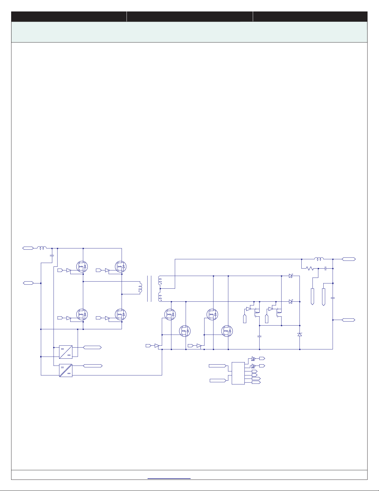
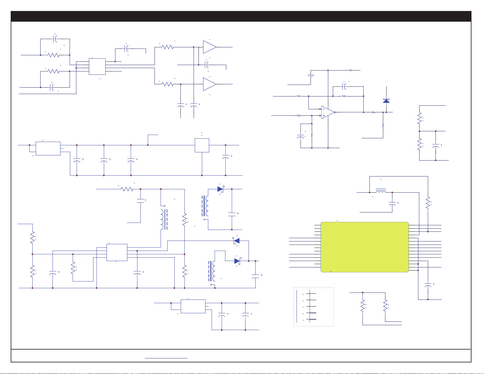
EPC9115
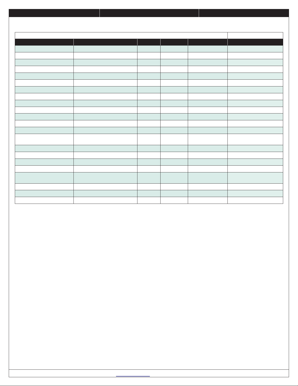
Table 2: Bill of Materials
Designator Description Quantity Value MFG MFGPN
C1, C2, C3, C4, C10, C11 Capacitor, 2.2 µF, 6.3 V, X5R 6
2.2
µ
F
TDK Corporation C1005X5R0J225M050BC
C12, C13, C17, C42, C43, C46, C47,
C50, C55, C58 Capacitor, 22 pF, 50 V, NPO, 5% 10
22 pF
Murata GRM1555C1H220JA01D
C14, C16 Capacitor, 4.7 µF, 6.3 V, X7S 2
4.7
µ
F
TDK C1608X7S0J475K080AC
C18 Capacitor, 1000 pF, 50 V, NPO, 5% 1
1000 pF
Murata GRM1555C1H102JA01D
C19 Capacitor, 0.1 µF, 50 V, X7R 1
100 nF, 50 V
TDK C1005X7R1H104K050BB
C20, C21, C22, C23, C24, C25, C51,
C54, C65, C67, C68, C69 Capacitor, 1 µF, 100 V, X7S 12
1
µ
F, 100 V
TDK C2012X7S2A105M125AE
C26 Capacitor, 0.047 µF, 25 V, X7R, 5% 1
0.047 µF, 25 V
Murata GRM155R71E473JA88D
C27, C28, C29, C30, C31, C32, C33,
C34, C35, C36, C37, C38 Capacitor, 4.7 µF, 25 V, X7R 12
4.7 µF, 25 V
TDK CGA4J1X7R1E475K125AC
C39 Capacitor. 3300 pF, 2000 V, X7R 1
3300 pF
Johanson 202S43W332KV4E
C40, C41, C44, C45, C48, C49, C52,
C53, C70, C71 Capacitor 10
0.22
µ
F
Murata GRM155R71C224KA12D
C5, C59, C61, C64, C66 Capacitor 4
0.1 µF, 100 V
Murata GRM188R72A104KA35D
C6, C9 Capacitor, 3.3 µF, 16 V, X5R 2
3.3 U
TDK Corporation C1608X5R1C335K
C60, C62 Capacitor 2
2.2 U
Samsung CL31B225KCHSNNE
C63 Capacitor 1
470 nF, 50 V
TDK CGA4J3X7R1H474K125AB
C7 Capacitor, 330 pF, 25 V, NPO, 5% 1
330 pF
Murata GRM1555C1E331JA01D
C8 Capacitor, 0.1 µF, 16 V, X7R 1
0.1
µ
F
Murata GRM155R71C104KA88D
D1, D2, D3 Schottky diode 3
BAT41K
ST Microelectronics BAT41KFILM
D6, D9 Schottky 60 V 1A 2
60 V, 1 A
Vishay MSS1P6-M3/89A
D7 Zener Diode 1
33 V, 10 mA
NXP BZX384-C33,115
J2 Programming connector 1
N/A
TE Connectivity
5520425-3
J3, J5, J6, J9, J10, J13 Test point 6
N/A
Keystone
5015
J4, J8 Power connector 2
N/A
Molex
399100102
J7, J14, J15, J16 Connector 4
N/A
Tyco 4-103185-0-02
L1 Inductor 1
180 Ω
TDK MPZ1608S181ATAH0
L2 Inductor 1
0.33
µ
F, 20 A
Abracon ASPI-7318-R33M-T
L3 470 nH, 62A inductor 1
470 nH
Vishay IHLP-6767GZ-01
Q1, Q2, Q3, Q4 eGaN FET, 80 V, 60 A, 2.5 mΩ 4 EPC EPC2021
Q13, Q14 NPN/PNP DFN PBSS4160PANP 2 NXP PBSS4160PANP,115
Q16 DUAL NPN DFN PBSS4160PAN 1 NXP PBSS4160PAN,115
Q5, Q6, Q7, Q8 eGaN FET, 60 V, 60 A, 2 mΩ 4 EPC EPC2020
Q9, Q10 P-Channel DMOS FET, -60 V,
1.6 A, logic level gate 2 Vishay SQ1421EEH-T1-GE3
R1, R19, R26, R33, R40, R42,
R43 Resistor 7 1R0 Yageo RC0402FR-071RL
R12, R13 Resistor, 1% 2 470 Vishay CRCW0402470RFKED
R14 Resistor, 0.1% 1 4.99 K, 0.1% Susumu RG1608P-4991-B-T5
R15, R46, R48, R51 Resistor, 0.1% 4 1 K, 0.1% Susumu RG1005P-102-B-T5
R2 Resistor 1 100 K Vishay CRCW0603100KFKEA
R20, R24, R27, R31, R34, R38,
R41, R45 Resistor 8 4.7 Yageo RC0402FR-074R7L
R21, R23, R28, R30, R37, R44,
R59, R60 Resistor 8 49.9 Yageo RC0402FR-0749R9L
R22, R25, R29, R32 Resistor 4 ZERO Vishay CRCW04020000Z0ED
R3, R4 Resistor 2 33.2 K Vishay RC0402FR-0733K2L