QUICK START GUIDE
EPC – EFFICIENT POWER CONVERSION CORPORATION | WWW.EPC-CO.COM | COPYRIGHT 2017 | | 5
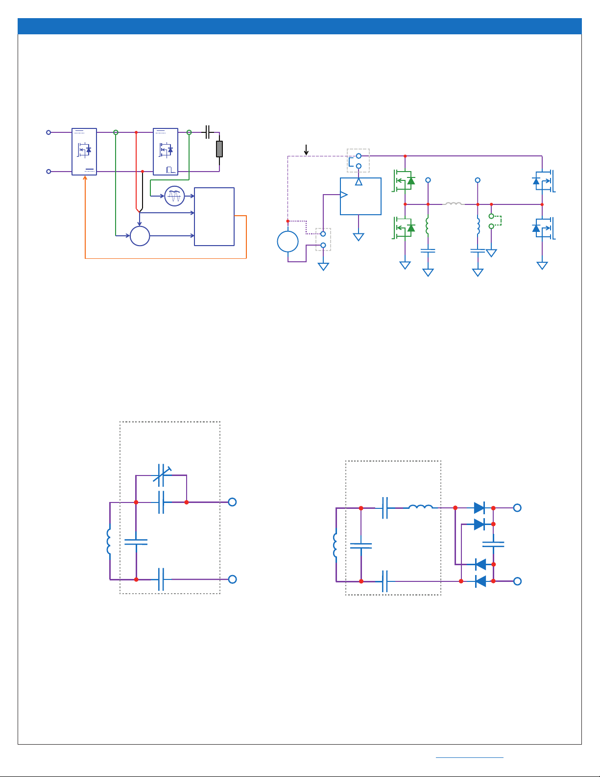
Demonstration System EPC9113
NOTE.
1. When measuring the high frequency content switch-node (Source Coil Voltage), care
must be taken to avoid long ground leads. An oscilloscope probe connection (preferred
method) has been built into the board to simplify the measurement of the Source Coil
voltage (shown in Figure 4).
2. To maintain control stability, the red LED for voltage mode indicator on the EPC9509
version 1.0 has been disabled. This will be corrected in subsequent revisions of the
board. For questions regarding this LED function, please contact EPC.
3. You may experience audible noise emanating from the inductor of the SEPIC converter.
This is due to a minor instability. This minor instability does not impact the performance
of the power amplier or the protection circuitry of the system.
4. AVOID using a Lab Benchtop programmable DC as the load for the category 3 device
board. These loads have low control bandwidth and will cause the EPC9113 system to
oscillate at a low frequency and may lead to failure. It is recommended to use a xed low
inductance resistor as an initial load. Once a design matures, a post regulator, such as a
Buck converter, can be used.
THERMAL CONSIDERATIONS
The EPC9113 demonstration system showcases the EPC2108 and
EPC2036 in a wireless energy transfer application. Although the
electrical performance surpasses that of traditional silicon devices,
their relatively smaller size does magnify the thermal management
requirements. The operator must observe the temperature of the gate
driver and eGaN FETs to ensure that both are operating within the
thermal limits as per the datasheets.
NOTE. The EPC9113 demonstration system has limited current and thermal protection
only when operating o the Pre-Regulator. When bypassing the pre-regulator there is no
current or thermal protection on board and care must be exercised not to over-current or
over-temperature the devices. Excessively wide coil coupling and load range variations can
lead to increased losses in the devices.
Pre-Cautions
The EPC9113 demonstration system has no enhanced protection
systems and therefore should be operated with caution. Some specic
precautions are:
1. Never operate the EPC9113 system with a device board that is A4WP
compliant as this system does not communicate with the device to
correctly setup the required operating conditions and doing so can
lead to the failure of the device board. Please contact EPC should
operating the system with an A4WP compliant device is required to
obtain instructions on how to do this. Please contact EPC at info@epc-
co.com should the tuning of the coil be required to change to suite
specic conditions so that it can be correctly adjusted for use with the
ZVS class-D amplier.
2. There is no heat-sink on the devices and during experimental
evaluation it is possible present conditions to the amplier that may
cause the devices to overheat. Always check operating conditions and
monitor the temperature of the EPC devices using an IR camera.
3. Never connect the EPC9509 amplier board into your VNA in an
attempt to measure the output impedance of the amplier. Doing so
will severely damage the VNA
QUICK START PROCEDURE
The EPC9113 demonstration system is easy to set up and evaluate the
performance of the eGaN FET in a wireless power transfer application. Refer
toFigure1 toassemble thesystem andFigures 6and 8for properconnection
and measurement setup before following the testing procedures.
The EPC9509 can be operated using any one of two alternative methods:
a. Using the pre-regulator
b. Bypassing the pre-regulator
a. Operation using the pre-regulator
The pre-regulator is used to supply power to the amplier in this mode
and will limit the coil current, power delivered or maximum supply volt-
age to the amplier based on the pre-determined settings.
The main 19 V supply must be capable of delivering 2 ADC. DO NOT turn
up the voltage of this supply when instructed to power up the board,
instead simply turn on the supply. The EPC9509 board includes a pre-
regulator to ensure proper operation of the board including start up.
1. Make sure the entire system is fully assembled prior to making electrical
connections and make sure jumper JP1 is installed. Also make sure the
source coil and device coil with load are connected.
2. With power o, connect the main input power supply bus to J1 as
shown in Figure 3. Note the polarity of the supply connector.
3. Make sure all instrumentation is connected to the system.
4. Turn on the main supply voltage to the required value (19 V)
5.
Once operation has been conrmed,
observe the output voltage
and other parameters on both the amplier and device boards.
6. For shutdown, please follow steps in the reverse order.
b. Operation bypassing the pre-regulator
In this mode, the pre-regulator is bypassed and the main power is
connected directly to the amplier. This allows the amplier to be
operated using an external regulator.
In this mode there is no protection for ensuring the correct operating
conditions for the eGaN FETs.
1. Make sure the entire system is fully assembled prior to making
electrical connections and make sure jumper JP1 has been removed
and installed in JP50 to disable the pre-regulator and to place the
EPC9509 amplier in bypass mode. Also make sure the source coil and
device coil with load are connected.
2. With power o, connect the main input power supply bus +VIN to the
bottom pin of JP1 and the ground to the ground connection of J1 as
shown in Figure 3.
3. With power o, connect the control input power supply bus to J1.
Note the polarity of the supply connector. This is used to power the
gate drivers and logic circuits.
4. Make sure all instrumentation is connected to the system.
5. Turn on the control supply – make sure the supply is 19 V range.
6. Turn on the main supply voltage to the required value (it is
recommended to start at 0 V and do not exceed the absolute
maximum voltage of 52 V).
7. Once operation has been conrmed, adjust the main supply
voltage within the operating range and observe the output voltage,
eciency and other parameters on both the amplier and device boards.
8. For shutdown, please follow steps in the reverse order. Start by
reducing the main supply voltage to 0 V followed by steps 6 through 2.