QUICK START GUIDE
4 | | EPC – EFFICIENT POWER CONVERSION CORPORATION | WWW.EPC-CO.COM | COPYRIGHT 2017
Demonstration System EPC9087
THERMAL CONSIDERATIONS
The EPC9087 development board showcases the EPC2037 eGaN FET.
The EPC9087 is intended for bench evaluation with low ambient
temperature and convection cooling. The addition of heat-sinking and
forced air cooling can signicantly increase the current rating of these
devices, but care must be taken to not exceed the absolute maximum
die temperature of 150°C.
NOTE.The EPC9087 development board does not have any current or
thermal protection on board.
For more information regarding the thermal performance of EPC eGaN
FETs, please consult:
D. Reusch and J. Glaser, DC-DC Converter Handbook, a supplement to GaN
Transistors for Ecient Power Conversion, First Edition, Power Conversion
Publications, 2015.
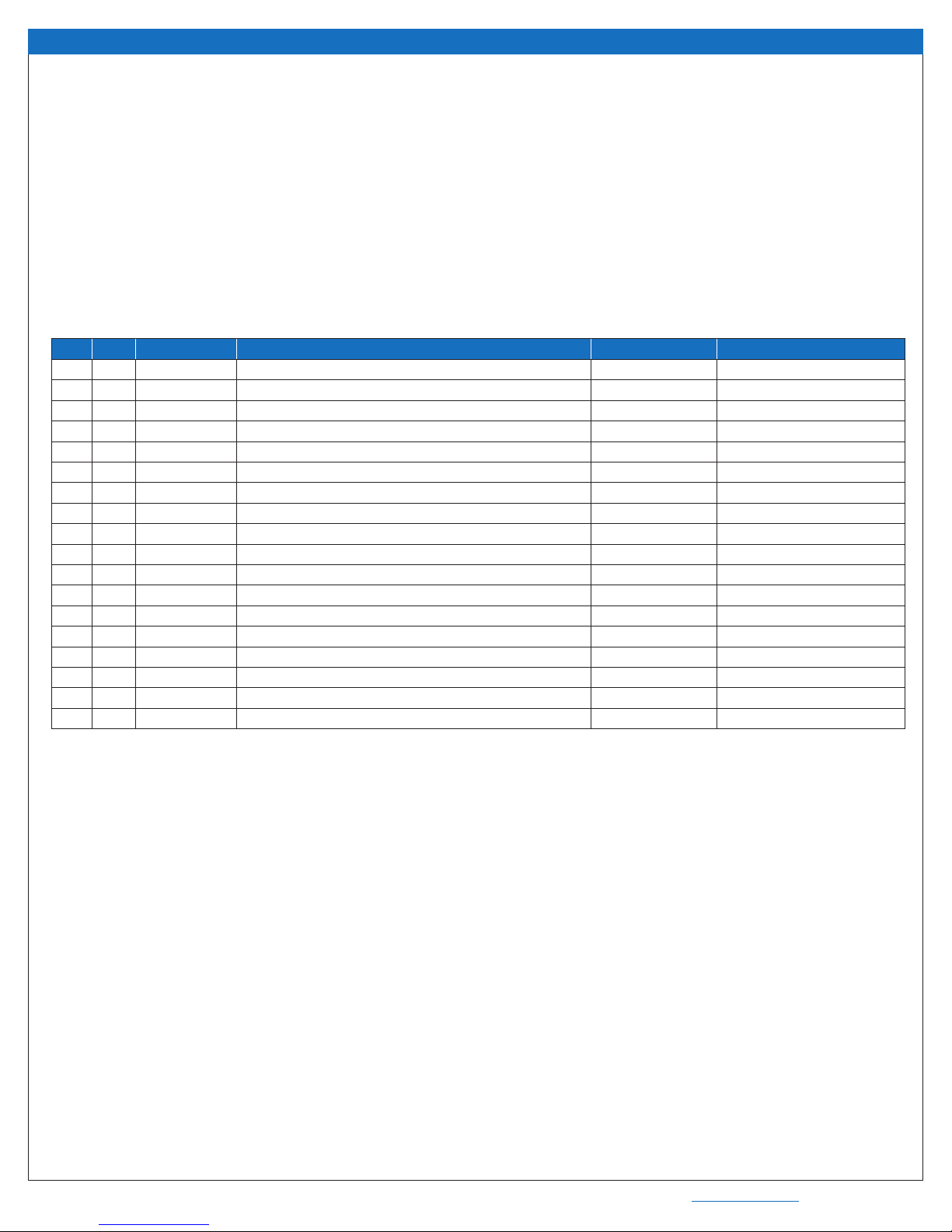
EPC9087 BOM
Item Qty Reference Part Description Manufacturer Part Number
1 1 C21 Capacitor, 1 µF, ±10%, 100 V, X7S TDK CGA4J3X7S2A105K125AE
2 3 C4, C10, C11, Capactior, 1 µF, ±10%, 25V, X5R Murata GRM188R61E105KA12D
3 2 C9, C19 Capacitor, 100 nF, ±10%, 25V, X5R TDK C1005X5R1E104K050BC
4 2 C16, C17 Capactior, 100 pF, ±5%, 50V, NP0 Murata GRM1555C1H101JA01D
5 1 R1 Resistor, 10.0 kΩ, ±1%, 1/8 W Stackpole RMCF0603FT10K0
6 1 R5 Resistor, 47 Ω, ±1%, 1/8 W Stackpole RMCF0603FT47R0
7 1 R4 Resistor, 33.0 Ω, ±1%, 1/8 W Stackpole RMCF0603FT33R0
8 2 R2, R15 Resistor, 0 Ω, 1/8 W, Jumper Panasonic ERJ-3GEY0R00V
9 4 R19, R20, R23, R24 Resistor, 1 Ω, 1/16 W, Jumper Stackpole RMCF0402FT1R00
11 2 D1, D2 Schottky Diode, 30 V, 370 mV @ 1 mA, 30 ma Diodes Inc SDM03U40-7
10 2 Q1, Q2 eGaN® FET, 100V , 1.7A, 550 mΩ EPC EPC2037
12 1 U3 5 V LDO, 250 ma, up to 16 V In, Vdropout=0.33V @ 250 mA Microchip MCP1703T-5002E/MC
13 1 U2 Gate driver , 5.2 VDC, 1.2 A Texas Instruments LM5113TME/NOPB
14 1 U1 I.C., Logic 2 NAND Gate, 1.65 V to 5.5 V Fairchild NC7SZ00L6X
15 1 U4 2 input NAND Gate, tiny Logic Fairchild NC7SZ08L6X
16 2 TP1, TP2 Test Point, Subminiature Keystone 5015
17 0.19 TP3, J1, J2, J9 Connector, Male Vertical, 36 Pin. 230" Contact Height, .1" Center Pitch FCI 68001-236HLF
18 1 J3, J4, J5, J6, J7, J8 Connector, 24 Pin Male Header 0.1" Pitch FCI 68602-224HLF