Sony MZ-NH600 User manual

SERVICE MANUAL
PORTABLE MINIDISC RECORDER
AEP Model
E Model
SPECIFICATIONS
MZ-NH600
Audio playing system
MiniDisc digital audio system
Laser diode properties
Material: GaAlAs
Wavelength: λ= 790 nm
Emission duration: continuous
Laser output: less than 44.6 µW
(This output is the value measured at a distance
of 200 mm from the lens surface on the optical
pick-up block with 7 mm aperture.)
Recording and playback time
When using HMD1G (1GB disc):
Maximum 34 hours in Hi-LP stereo
When using MDW-80 in Hi-MD mode:
Maximum 10 hours and 10 min. in Hi-LP
stereo
When using MDW-80 in MD mode:
Maximum 160 min. in monaural
Maximum 320 min. in LP4 stereo
Revolutions
350 rpm to 3,000 rpm (CLV)
Error correction
Hi-MD:
LDC (Long Distance Code)/BIS (Burst
Indicator Subcode)
MD:
ACIRC (Advanced Cross Interleave Reed
Solomon Code)
Sampling frequency
44.1 kHz
Sampling rate converter
Input: 32 kHz/44.1 kHz/48 kHz
Coding
Hi-MD:
ATRAC3plus (Adaptive TRansform Acoustic
Coding 3 plus)
MD:
ATRAC
ATRAC3 −LP2/LP4
Modulation system
Hi-MD:
1-7RLL (Run Length Limited)/PRML
(Partial Response Maximum Likelihood)
MD:
EFM (Eight to Fourteen Modulation)
Frequency response
20 to 20,000 Hz ±3 dB
Inputs
LINE IN (OPT)1):
stereo mini-jack for analog input
(minimum input level 49 mV)
optical (digital) mini-jack for optical (digital)
input
Outputs
i: stereo mini-jack
Maximum output (DC)
Headphones:
3 mW + 3 mW (16 Ω) (European models)
5 mW + 5 mW (16 Ω) (Other models)
Power requirements
One LR6 (size AA) alkaline battery
AC power adaptor DC 3V
Operating temperature
+5°C (+41°F) to +35°C (+95°F)
1)The LINE IN (OPT) jack is used to connect
either a digital (optical) cable or a line
(analog) cable.
Battery life2)
Hi-MD mode (When using a 1GB Hi-MD disc)
(Unit: approx.hours)(JEITA3))
2) When using a new Sony LR6 (size AA) alkaline
dry battery (produced in Japan)
3) Measured in accordance with the JEITA
(Japan Electronics and Information Technology
Industries Association) standard.
When Linear
PCM Hi-SP Hi-LP
Recording
continuously 2.5 3.5 4.5
Playing
continuously 11.0 18.5 21.5
Ver 1.0 2004.05
US and foreign patents licensed from Dolby
Laboratories. Model Name Using Similar Mechanism NEW
MD Mechanism Type MT-MZNH900-181
Optical Pick-up Name ABX-U
9-877-840-01
2004E05-1
© 2004.05
Sony Corporation
Personal Audio Company
Published by Sony Engineering Corporation
•SonicStage, MD Simple Burner, OpenMG, “Magic Gate”, “MagicGate Memory Stick”,
“Memory Stick”, Hi-MD, Net MD, ATRAC, ATRAC3, ATRAC3plus and their logos are
trademarks of Sony Corporation.
•Microsoft, Windows, Windows NT and Windows Media are trademarks or registered
trademarks of Microsoft Corporation in the United States and /or other countries.
•IBM and PC/AT are registered trademarks of International Business Machines Corporation.
•Macintosh is a trademark of Apple Computer, Inc. in the United States and/or other countries.
•MMX and Pentium are trademarks or registered trademarks of Intel Corporation.
•All other trademarks and registered trademarks are trademarks or registered trademarks of their
respective holders.
– Continued on next page –

2
MZ-NH600
Dimensions
Approx. 83.6 ×28.9 ×77.0 mm (w/h/d)
(3
3
/
8
×1
3
/
16
×3
1
/
8
in.) (excluding projecting
parts and controls)
Mass
Approx. 101 g (3.6 oz) (the recorder only)
Design and specifications are subject to change
without notice.
CD-ROM (SonicStage Ver. 2.0/MD Simple
Burner Ver. 2.0) (1)*
*Do not play a CD-ROM on an audio CD player.
Dedicated USB cable (1)
Headphones/earphones (1)
Clamp filters for the AC power adaptor (2)
Attach the clamp filters when using the optional
AC power adaptor
Supplid accessories
When using the optional AC power
adaptor AC-E30HG:
Before using the AC power adaptor
AC-E30HG, do the following procedure to
attach the clamp filters to the cord of the
AC power adaptor. (You must affix the
ferrite cores to comply with applicable
EMC standards.)
1Open the clamp filters.
2Wind the AC power cord into the clamp
filters as shown below.
3Close the clamp filters.
Maximum
length:
approx. 4 cm
Maximum length:
approx. 4 cm
Make sure the
clasps are
fully engaged.
Hi-MD mode (When using a 60/74/80-
minute standard disc)
(Unit: approx.hours)(JEITA)
MD mode
(Unit: approx.hours)(JEITA)
When Linear
PCM Hi-SP Hi-LP
Recording
continuously 5.0 8.0 9.5
Playing
continuously 9.5 17.0 20.0
When SP
Stereo LP2
Stereo LP4
Stereo
Recording
continuously 7.5 9.5 11.0
Playing
continuously 20.5 24.0 26.0
4)
4)

3
MZ-NH600
TABLE OF CONTENTS
1. SERVICING NOTES ............................................... 4
2. GENERAL ................................................................... 5
3. DISASSEMBLY
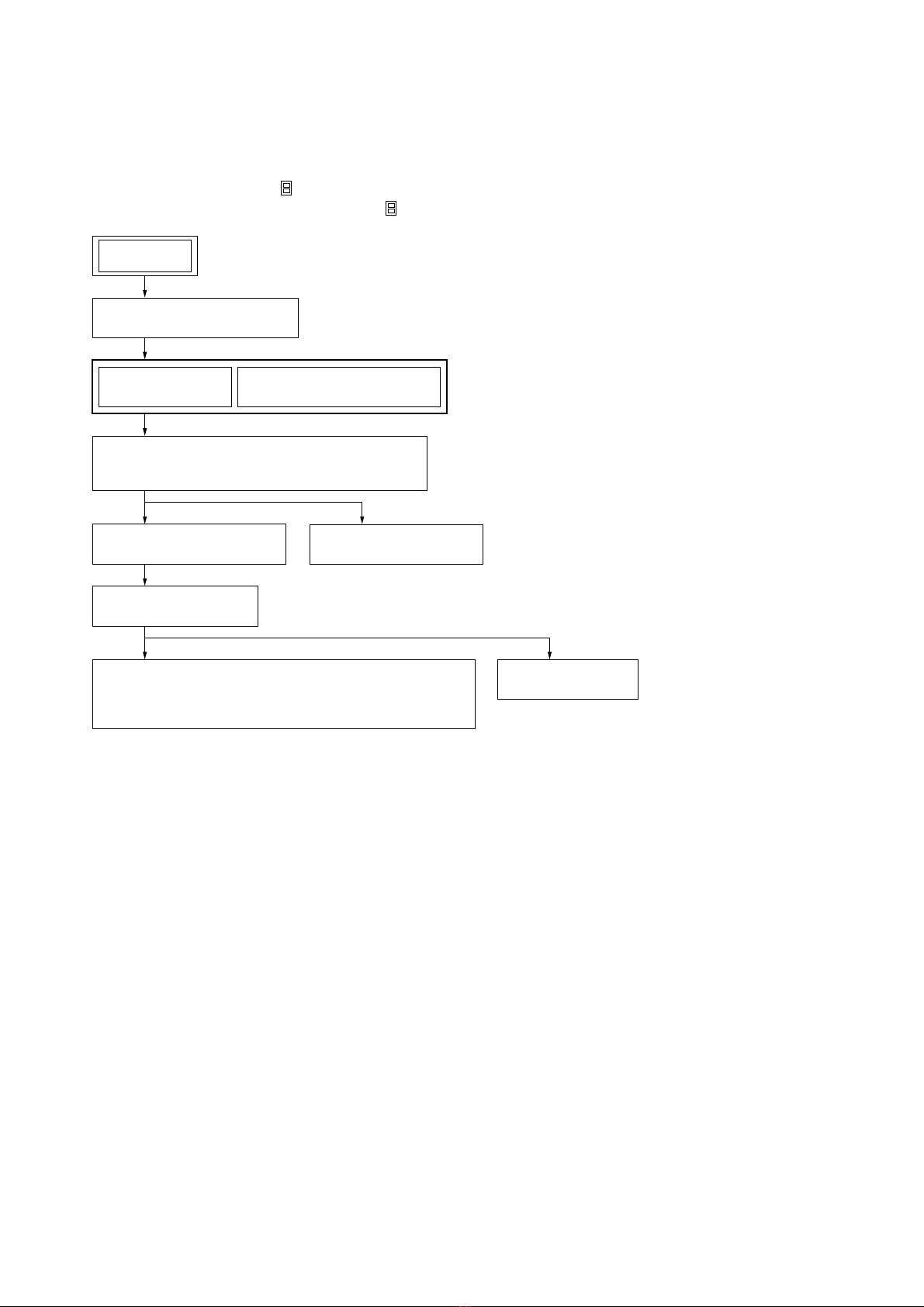
3-1. Disassembly Flow ........................................................... 6
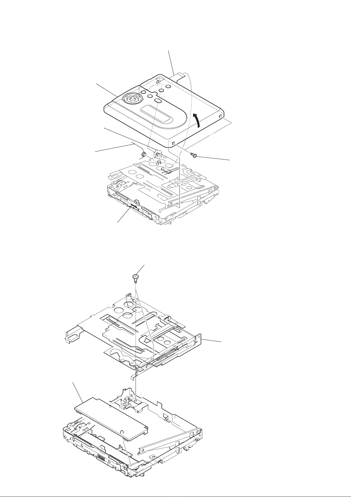
3-2. Case (Lower) Section ...................................................... 7
3-3. MAIN Board.................................................................... 7
3-4. Case (Upper) Section....................................................... 8
3-5. Mechanism Deck Section (MT-MZNH900-181),
MD Standard Pin ............................................................. 8
3-6. Set Chassis Assy .............................................................. 9
3-7. Gear (BSA), Gear (SB) ................................................... 9
3-8. Op Service Assy .............................................................. 10
3-9. DC Motor SSM18D/C-NP (Spindle) (M701),
DC Motor (Sled) (M702), DC Motor Unit
(Over Write Head Up/Down) (M703) ............................. 10
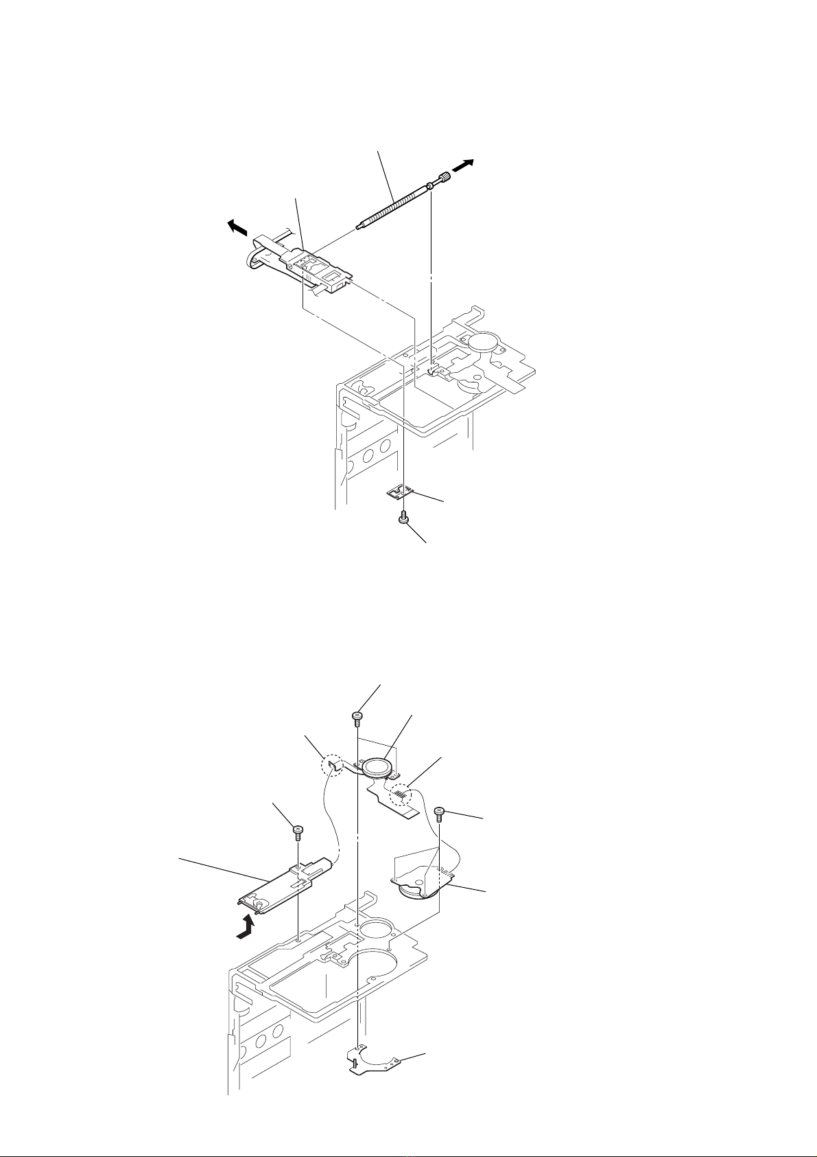
3-10. Holder Assy ..................................................................... 11
4. DIAGRAMS
4-1. Block Diagram –MD SERVO Section – ......................... 13
4-2. Block Diagram –AUDIO Section –................................. 14
4-3. Block Diagram –POWER SUPPLY Section – ................ 15
4-4. Schematic Diagram –MAIN Section (1/9) – ................... 17
4-5. Schematic Diagram –MAIN Section (2/9) – ................... 18
4-6. Schematic Diagram –MAIN Section (3/9) – ................... 19
4-7. Schematic Diagram –MAIN Section (4/9) – ................... 20
4-8. Schematic Diagram –MAIN Section (5/9) – ................... 21
4-9. Schematic Diagram –MAIN Section (6/9) – ................... 22
4-10. Schematic Diagram –MAIN Section (7/9) – ................... 23
4-11. Schematic Diagram –MAIN Section (8/9) – ................... 24
4-12. Schematic Diagram –MAIN Section (9/9) – ................... 25
4-13. Printed Wiring Board –MAIN Section (1/2) – ................ 26
4-14. Printed Wiring Board –MAIN Section (2/2) – ................ 27
5. EXPLODED VIEWS
5-1. Case (Lower) Section ...................................................... 40
5-2. Case (Upper) Section....................................................... 41
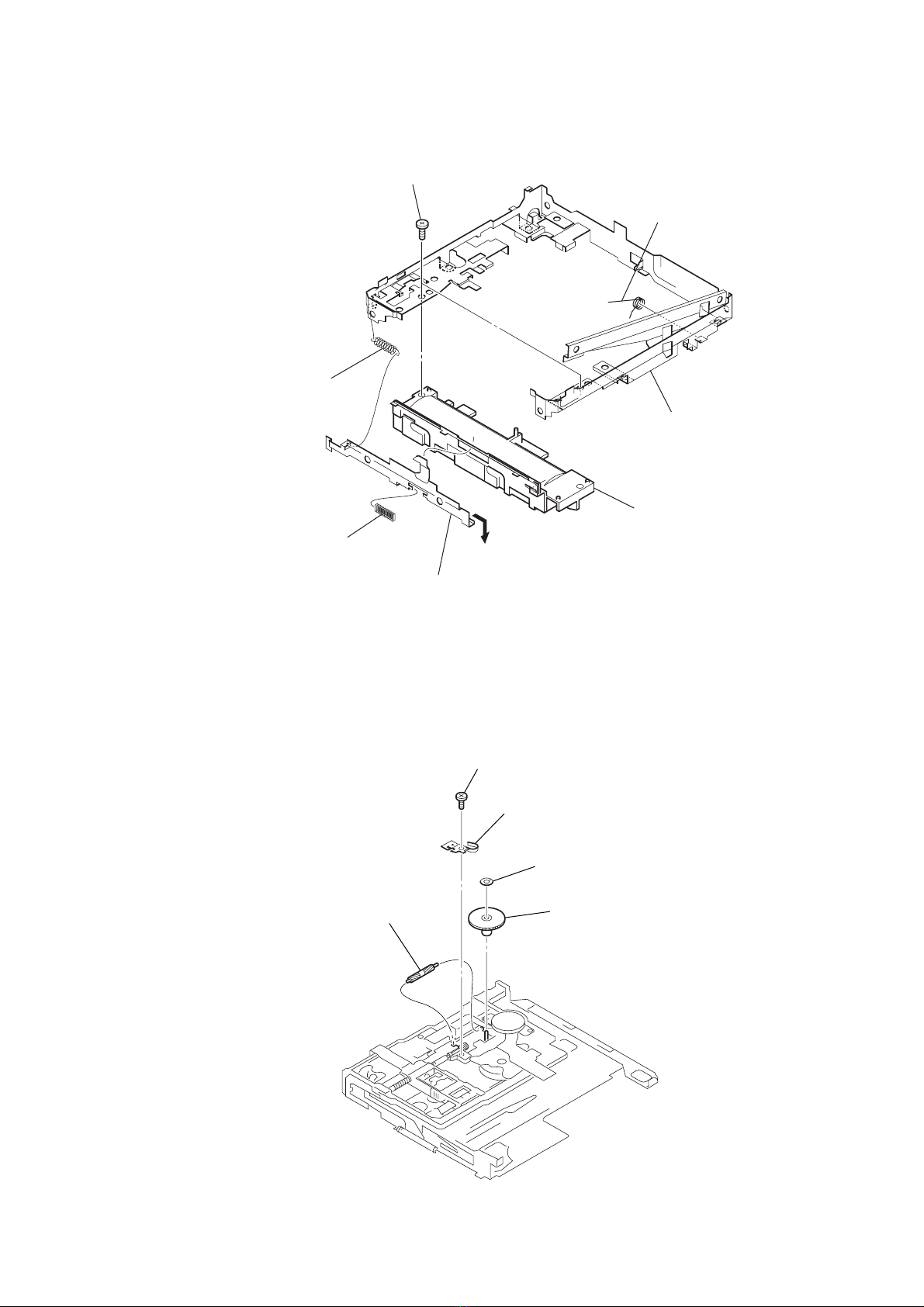
5-3. Chassis Section................................................................ 42
5-4. Mechanism Deck Section (MT-MZNH900-181) ............ 43
6. ELECTRICAL PARTS LIST................................ 44
Notes on chip component replacement
•Never reuse a disconnected chip component.
•Notice that the minus side of a tantalum capacitor may be
damaged by heat.
Flexible Circuit Board Repairing
•Keep the temperature of the soldering iron around 270 ˚C
during repairing.
•Do not touch the soldering iron on the same conductor of the
circuit board (within 3 times).
•Be careful not to apply force on the conductor when soldering
or unsoldering.
CAUTION
Use of controls or adjustments or performance of procedures
otherthanthose specifiedhereinmayresultinhazardous radiation
exposure.
UNLEADED SOLDER
Boards requiring use of unleaded solder are printed with the lead-
free mark (LF) indicating the solder contains no lead.
(Caution: Some printed circuit boards may not come printed with
the lead free mark due to their particular size)
: LEAD FREE MARK
Unleaded solder has the following characteristics.
•Unleaded solder melts at a temperature about 40 °C higher
than ordinary solder.
Ordinary soldering irons can be used but the iron tip has to be
applied to the solder joint for a slightly longer time.
Soldering irons using a temperature regulator should be set to
about 350 °C.
Caution: The printed pattern (copper foil) may peel away if
the heated tip is applied for too long, so be careful!
•Strong viscosity
Unleaded solder is more viscou-s (sticky, less prone to flow)
than ordinary solder so use caution not to let solder bridges
occur such as on IC pins, etc.
•Usable with ordinary solder
It is best to use only unleaded solder but unleaded solder may
also be added to ordinary solder.
SAFETY-RELATED COMPONENT WARNING!!
COMPONENTS IDENTIFIED BY MARK 0 OR DOTTED LINE
WITH MARK 0ON THE SCHEMATIC DIAGRAMS AND IN
THE PARTS LIST ARE CRITICAL TO SAFE OPERATION.
REPLACE THESE COMPONENTS WITH SONY PARTS WHOSE
PART NUMBERS APPEAR AS SHOWN IN THIS MANUAL OR
IN SUPPLEMENTS PUBLISHED BY SONY.

4
MZ-NH600
The laser diode in the optical pick-up block may suffer electrostatic
break-down because of the potential difference generated by the
charged electrostatic load, etc. on clothing and the human body.
During repair, pay attention to electrostatic break-down and also
use the procedure in the printed matter which is included in the
repair parts.
The flexible board is easily damaged and should be handled with
care.
NOTES ON LASER DIODE EMISSION CHECK
The laser beam on this model is concentrated so as to be focused on
the disc reflective surface by the objective lens in the optical pick-
up block. Therefore, when checking the laser diode emission,
observe from more than 30 cm away from the objective lens.
OPERATION CHECK WHEN THE LID IS OPEN
Inperforming the repair with the powersuppliedto the set, removing
the MAIN board causes the set to be disabled.
Insuch a case, makea solder bridge to short SL894 (OPEN/CLOSE)
on the MAIN board in advance.
NOTES ON HANDLING THE OPTICAL PICK-UP
BLOCK OR BASE UNIT
SECTION 1
SERVICING NOTES
SL894
(OPEN/CLOSE)
– MAIN Board (Conductor Side) –
Providing the required system environment
The following system environment is required in order to use the SonicStage Ver. 2.0/MD
Simple Burner Ver. 2.0 software for the MD Walkman.
This software is not supported by the following environments:
•OSs other than the indicated above
•Personally constructed PCs or operating systems
•An environment that is an upgrade of the original manufacturer-installed operating system
•Multi-boot environment
•Multi-monitor environment
•Macintosh
•We do not ensure trouble-free operation on all computers that satisfy the system requirements.
•The NTFS format of Windows XP/Windows 2000 Professional can be used only with the standard
(factory) settings.
•We do not ensure trouble-free operation of the system suspend, sleep, or hibernation function on all
computers.
•For Windows 2000 Professional users, install Service Pack 3 or later version before using the
software.
System requirements
Computer IBM PC/AT or Compatible
•CPU: Pentium II 400 MHz or higher (Pentium III 450 MHz or higher
is recommended.)
•Hard disk drive space: 200 MB or more (1.5 GB or more is
recommended) (The amount space will vary according to Windows
version and the number of music files stored on the hard disk.)
•RAM: 64 MB or more (128 MB or more is recommended)
Others
•CD drive (capable of digital playback by WDM)
•Sound Board
•USB port (supports USB (previously USB 1.1))
Operating
System Factory installed:
Windows XP Media Center Edition 2004/Windows XP Media Center
Edition/Windows XP Professional/Windows XP Home Edition/
Windows 2000 Professional/Windows Millennium Edition/Windows
98 Second Edition
Display High Color (16bit) or higher, 800 ×600 dots or better (1024 × 768 dots
or better is recommended)
Others •Internet access: for Web registration, EMD services and CDDB
•Windows Media Player (version 7.0 or higher) installed for playing
WMA files
Notes

5
MZ-NH600
SECTION 2
GENERAL This section is extracted from
instruction manual.
Looking at controls
The recorder
Ax(stop) CANCEL button
BOPEN switch
CDisplay window
DT MARK/REC (+N) button
ENAVI/ MENU button
Press lightly to go to the NAVI
(navigation) setting mode
Press for 2 seconds or more to go to
the MENU setting mode.
FGROUP button
GDC IN 3V jack
When you use the optional AC power
adaptor, connect it to this jack.
HX(pause) button
IJog dial
J5-way control key
Operation Function
Press NENT
1)
1) Thereare tactiledotsbesidethe
N
ENT
and
VOL +
buttons.
play, enter
Press towards
.find the beginning
of the previous
track, rewind
Press towards
>find the beginning
of the next track,
fast forward
Press towards
VOL +
1)
or
VOL −.
volume
KUSB cable connecting jack
LLINE IN (OPT) jack
MBattery compartment (at the bottom)
NHOLD switch
Slide the switch in the direction of the
arrow to disable the buttons on the
recorder. To prevent the buttons from
being accidentally operated when you
carry the recorder, use this function.
Oi(headphones/earphones) jack
The display window of the recorder
ACharacter information display
Displays the disc and track names,
date, error messages, track numbers,
etc.
BSYNC (synchro-recording) indication
CHi-MD/MD indication
“Hi-MD” lights up when the
operation mode of the recorder is in
Hi-MD mode and “MD” lights up
when the operation mode is in MD
mode.
DREC indication
Lights up during recording or file
transfers from the computer. When
flashing, the recorder is in record
standby mode.
EBattery indication
Shows the approximate remaining
battery power. If the battery is weak,
the indication becomes empty and
starts flashing.
FDisc indication
Shows that the disc is rotating for
recording or playing.
GTrack mode (PCM, Hi-SP, Hi-LP, SP,
LP2, LP4, MONO) indication
HSub play mode/Repeat play
indications
Shows the selected Sub play mode
(single-track play, shuffle play, etc.) or
Repeat play.
IMain play mode indications
Shows the selected main play mode
(group play, bookmark play, etc.).
123456
78 9

MZ-NH600
6
•This set can be disassembled in the order shown below.
3-1. DISASSEMBLY FLOW
SECTION 3
DISASSEMBLY
3-2. CASE (LOWER) SECTION
(Page 7)
3-3. MAIN BOARD
(Page 7) 3-4. CASE (UPPER) SECTION
(Page 8)
3-5. MECHANISM DECK SECTION (MT-MZNH900-181),
MD STANDARD PIN
(Page 8)
3-7. GEAR (BSA), GEAR (SB)
(Page 9)
3-8. OP SERVICE ASSY
(Page 10)
3-9. DC MOTOR SSM18D/C-NP (SPINDLE) (M701),
DC MOTOR (SLED) (M702),
DC MOTOR UNIT (OVER WRITE HEAD UP/DOWN) (M703)
(Page 10)
3-10. HOLDER ASSY
(Page 11)
3-6. SET CHASSIS ASSY
(Page 9)
SET
Note 1: The process described in can be performed in any order.
Note 2: Without completing the process described in , the next process can not be performed.

MZ-NH600
7
3-3. MAIN BOARD
2
LCD module flexible board
(CN471)
6
three screws
(M1.4)
1
Remove two solders of over
write head flexible board.
8
OP flexible board
(CN501)
3
motor flexible board
(CN701)
9
MAIN board
5
leaf spring (USB)
4
screw (M1.4)
7
3-2. CASE (LOWER) SECTION
2
Remove the case (lower) section
in the direction of the arrow.
1
two screws
(M1.4)
1
two screws
(M1.4)

MZ-NH600
8
3-4. CASE (UPPER) SECTION
1
LCD module flexible boaed
(CN471)
7
case (upper) section
6
boss
3
herical torsion
spring (L)
2
Open the case (upper) section.
4
two step screws
5
3-5. MECHANISM DECK SECTION (MT-MZNH900-181), MD STANDARD PIN
2
mechanism deck section
(MT-MZNH900-181)
3
MD standard pin
1
two step screws (MD)

MZ-NH600
9
3-6. SET CHASSIS ASSY
3-7. GEAR (BSA), GEAR (SB)
1
torsion coil spring (R)
2
extension spring (R)
5
two screws
3
compression coil spring (open)
4
open slider
6
battery case
7
set chassis assy
1
self tap screw
2
thrust retainer spring
3
washer (0.8-2.5)
4
gear (BSA)
5
gear (SB)

MZ-NH600
10
3-8. OP SERVICE ASSY
3-9. DC MOTOR SSM18D/C-NP (SPINDLE) (M701), DC MOTOR (SLED) (M702),
DC MOTOR UNIT (OVER WRITE HEAD UP/DOWN) (M703)
3
Remove lead screw block assy.
4
OP service assy
2
rack spring
1
screw (M1.4)
3
two screws (M1.4)
4
DC motor (sled)
(M702)
1
Remove four solders of flexible board.
2
Remove two solders of flexible board.
6
three self tap screws
7
DC motor SSM18D/C-NP
(spindle) (M701)
5
motor base assy
9
DC motor unit
(over write head up/down)
(M703)
8
self tap screw

MZ-NH600
11
3-10. HOLDER ASSY
4
Remove the holder assy
to the direction of the arrow
A
.
3
Open the holder assy.
1
boss
2
boss
A

MZ-NH600
12
MEMO

MZ-NH600
1313
SECTION 4
DIAGRAMS
4-1. BLOCK DIAGRAM – MD SERVO Section –
8
48
47
40
41
42
23
9
35
21
32
33
7
56
1
54
55
50
51
52
49
15
14
18
19
IY
VREF
OPTICAL
PICK-UP
BLOCK
(ABX-U)
HR601
OVER
WRITE
HEAD
D
D_C
PD_I
PDO_SOURCE
C
B
A
VREF10
A_C
JY
JX
IX
IY RFO
PEAK
BOTM
ABCD
FE
TE
ADFG
PD-NI
VREF09
SBUS
SCK
S-MON
XRESET
RF AMP, FOCUS/TRACKING ERROR AMP
IC501
M703
OVER WRITE
HEAD
UP/DOWN
17
IX
JX
JY
A
B
C
D
S0
S1
L2
TRK+
FCS+
FCS–
FCS+
FCS–
TRK–
TRK+
TRK–
101
106
107
108
109
114
153
110
225
113
252
209
210
251
142
77
84
82
60
62
169
170
164
165
166
160
232
168
167
172
216
157
156
154
155
20
19
29
30
162
163
28
48
49
50
64
1
3
54 53 52
55 238
26
46
27
25
63
62
22
23
24
21
182
IIN
PD_BUF
20
F
OVER WRITE
HEAD DRIVE
Q601, 602
MM
HB
OUTA
OUTB
CLK
EFM
EFMO
OVER WRITE HEAD DRIVE
IC601 (1/2)
RFI TO IC801 (2/3)
(AUDIO SECTION)
145 VIN
PEAK
BOTM
ABCD
FE
TE
ADFG
VC
XRF_RST
SE
SSB_CLK
PF1/S0DO
PF2/S1DO
SSB_DATA
38
45
OFTRK
VC 123
180
VREF_MON
OFTRK
APCREF_DA
SYSTEM CONTROLLER,
DIGITAL SIGNAL PROCESSOR
IC801 (1/3)
A
CLK
SLCU
SLCV
SPCU
SPCV
SPCW
SLD MON U
SLD MON V
CLV MON U
CLV MON V
CLV MON W
SPRD
SPDL_MON
SLDW
SLDV
SRDR
SLD_MON
FRDR
FFDR
TRDR
TFDR
SPDV
SPDW
XRST_MTR_DRV
RI1
FI1
RI2
FI2
WI2
VI2
UI2
VI1
WI1
CPWO2
CPVO2
CPUO2
SLD MON W
SLD MON V
SLD MON U
STALL
UI1
PWM1
FO2
FCS–
FCS+
TRK–
TRK+
COM2
WO1
CPVI2
WO2
CPUI2
CPWI2
CPUI1
CPVI1
CPWI1
COM1
FOCUS/TRACKING
COIL DRIVE,
SPINDLE/SLED
MOTOR DRIVE
IC701
M701
(SPINDLE)
11 RF_IY
10 RF_IX
26
CLK 174 FS256_OUT
PLSE_XDC
CONT
254
272
LDPEN
XLSRCK
158
FS4
59 60 61
CPWO1
CPVO1
CPUO1
CLV MON W
CLV MON V
CLV MON U
15951 SFDR
PWM2
28945 HI_Z_SLO
ST2
2904 HI_Z_SPDL
ST1
63
175
EFM_CLK
CHOPPERCLK
56
245
LATCH
XCS_REC_DRV
69 HBB
78 HB
70 HBA
U
WV
M702
(SLED)
U
WV
171SLCW SLD MON W
161 SPFD
NPPO 43
ADIP_IN 39
12 RF_JX
13 RF_JY
RF BUFFER
Q504
•SIGNAL PATH
: PLAYBACK
: REC
L2 B+
L1 L1 B+
VCC REG3 B+
PVCC REG2 B+
MVCC MDVCC
32, 33
UO2
39, 40
UO1
9, 10
VO1
6, 7
VO2
42, 43
RO2
35, 36
FO1
16, 17
RO1
13, 14
(Page 15)

MZ-NH600
1414
+1.2V
REGULATOR
IC302
REFERENCE VOLTAGE
SWITCHING
Q351
SYSTEM CONTROLLER,
DIGITAL SIGNAL PROCESSOR
IC801 (2/3)
XMUTE/MUTE
211
212
PF3/RTG3
199BEEP
314UDP
318UPUEN
315UDM
3
2
DATA+
DATA–
1VBUS
CN451
(USB)
320
UOSCO
319
UOSCI
X801
48MHz
311
OSCO
239XCS_NV
310
OSCI
X802
22.5792MHz
195SI0
196SO0
197SCK0
2
24
4
23
22
21
1517 18
HEADPHONE
AMP
IC352
OUTA
OUTB
BEEP_OUTA
BEEP_OUTB
7
SDT0
VREF_IN
INA
INB
PW_SW
MT_SW
BEEP_IN
28 LIN
1RIN
3
AVDD
13
SDO0
SCK0
F
SDO0, SCK0
E
VBUS
B
XRST2
C
XWK1, XWK2,
XWK4
J352
i
1
2
3
4
XCS
SCK
DI
DO
EEPROM
IC892
•SIGNAL PATH
: PLAYBACK
: REC
: OPTICAL IN
: LINE IN
: USB CHECK OUT
: USB CHECK IN
RVDD
D
RMC KEY
RVDD
DTCK
KEY-R
RGND
313DTCK
131RMC_KEY
147
AOUTL
148
AOUTR
173 DIN
208 XOPT_CTL
185 OPT_DET
J301
186 XJACK_DET
307 ADDT
306 FS256
309 XBCK
308 LRCK
190 XPD_ADC
196 SO0
197 SCK0
189 XCS_ADC
REG1 B+
A/D CONVERTER
IC301
FROM IC801 (1/3)
(MD SERVO SECTION)
B+ SWITCH
Q301
9
MCLK
8
BCLK
10
LRCK
14
PDN
11
CDTI
12
CCLK
13
CSN
VC01 B+
LINE IN
(OPTICAL)
224
SL801
(TEST)
XTEST
DDC3 B+
133
REC_KEY/DOWNLOAD
248
JOG_A
249
JOG_B
227
XHOLD_SW
183
PAUSE_KEY
124
SET_KEY_1
125
SET_KEY_2
213
SI1
214
SO1
215
SCK1
236
XCS_LCD
192
XRST_LCD
RESET
SWITCH
Q471
T_MARK
JOG_A
JOG_B
HOLD
PAUSE
SET_KEY_1
SET_KEY_2
SDI
SDO
SCK
CS
LCD
MODULE
RST
XWK
DVDD
XWK1
XWK4
DDC3 B+
REG VSTB B+
+2.4V
REGULATOR
IC471
253
S894–2
Hi-MD
PROTECT
DETECT
HIMD_PROTECT
188
S893
OPEN/CLOSE
DETECT
OPEN_CLOSE_SW
184
S894–1
PROTECT
DETECT
PROTECT
–1 –2
135
S892
HALF
LOCK
XWK2
HALF_LOCK_SW/
OPEN_SW
VB B+
193 USB_WAKE
WAKE UP SWITCH
Q803
128
WK_DET
4-2. BLOCK DIAGRAM – AUDIO Section –
(Page 15)
(Page 15)
(Page 15)
(Page 15)
(Page 15)

MZ-NH600
1515
(Page 14)
(Page 14)
4-3. BLOCK DIAGRAM – POWER SUPPLY Section –
246
SYSTEM CONTROLLER
IC801 (3/3)
GND_SW
226VREC_SEL
VBUS_VB_CTL
25
LG
VCO1
11
7
LVB
27
VB
14
L1
13
L1
38
L2
37
L2
DW_2B
DW_2T
55
REGI1
52
REGI2
48
REGI3
44
43
VRMC 6
DATA
SDO0
SCK0
SLEEP
58 CLK 63
XWK3 3
64
STRB
59
SCK
60
XWK2 4
XWK4 2
VG
23
RVDD
VC1
10
VO1
12
VC
B+
VG
B+
VC01
B+
VCO2
B+
VSTB
B+
DDC3 B+
REGO2
51
REG2 B+
REGO1
54
REG1 B+
RVDD
VREF
57
VSTB
9
VCO2
40
REGO3
47
RF1 26
BAT+ 31
VO 32
VI 6
IN1– 12
I_CTL1 20
BAT– 25
NI_VI_CTL
CHARGE CONTROL
IC401
4
CHG_PWM 7
CHG_I_CTL2 29
CHG_I_CTL3 23
CHG_MON
VI_CTL
CHG_CTL
I_CTL2
I_CTL3
A/D
TYPE2
22
CHG_TYPE2
16
REG3 B+
MDVCC
VREC B+
218 233
YUZU_SLEEP
XCS_PWR_IC
181
RECP
231
RECP_MON
XRST2
34
XRST1
17
229
XRST2_DET
XRST2
POWER CONTROL
IC601 (2/2)
83
VG
101
TSBV_IN
97
REG_IN
90
DVDD_IN
105
VSTB_IN
18
VREF_IN
112
VREC
4
VRECO_2
5
VRECO_1
10
UP_1B
9
UP_1T
81
VREC_IN
80
VREC_IN
6
L1_2
7
L1_1
6
L1_2
7
L1_1
46
POWFB
SDO0
SCK0
SDO0 SCK0
F
B
CLK
A
XWK1, XWK2,
XWK4
C
REC KEY
D
129VBUS_MON VBUS B+
127HIDC_MON DC IN B+
121VB_MON VB B+
DRY BATTERY
SIZE "AA"
(IEC DESIGNATION R6)
1PC. 1.5V
299
PWM_L1
RESET SIGNAL
GENERATOR
IC902
+1.2V
REGULATOR
IC604
VOLTAGE
DETECT
IC606
RESET
SWITCH
Q618
VOLTAGE
DETECT
IC607
OR GATE
IC605
WAKE UP SWITCH
Q902
136
XRST
141
DACVREFH
5
XWK1
CHARGE ON/OFF
CONTROL
Q407
VBUS
D401
B+ SWITCH
Q901
B+ SWITCH
Q352, 353
B+ SWITCH
Q502, 503
REG4 B+
B+ SWITCH
Q616, 617
87 64 94 59 58
RST_OUT
VBUSSEL2
SLEEP_IN
DATA
SCK
54
VBUS
36
VPDRV
88
PVBUS
43
VBUSSEL
38
CLP
42
CLM
37
POWP1
41
POWP2
91 DVDD_OUT
REG5 B+
+3.2V
REGULATOR
IC603
98 REG_OUT
+1.2V
REGULATOR
IC602
REG5 OSC B+
REG F B+
93 OSC_OUT
+2.5V
REGULATOR
IC804
USB IF VDD 108 V33RO
12 VC
VC B+
D609 D610
61 VIF
13 VC
67 RECP
250
VBUS_DET 51 VBUS_DET
316
USBHOLD 86 HOLD_OUT
317
SUSPEND 99 SUS_IN
132
RST_CONT 95 RST_IN
REG5 VSTB B+ 106 VSTB_OUT
REG5 TSBV B+ 102 TSBV_OUT
D611
22 V3O_2
DDC3 B+
L1 B+
L2 B+
21 V3O_1
28 V3FB
66 VG2
73 VG3
B+ SWITCH
Q609
2
DW_1B
17
UP_3B
3
DW_1T
B+ SWITCH
Q603
25
L3_2
24
L3_1
B+ SWITCH
Q614, 615
B+ SWITCH
CONTROL
Q613
205
B+ SWITCH
Q611
B+ SWITCH
Q801, 802
SWITCHING
Q612
B+ SWITCH
Q608
DC IN DETECT
Q607
REGULATOR
Q401
DC IN DETECT
Q433
GROUND LINE
SWITCHING
Q403, 406
300
PWM_L2
Q501
E
VOLTAGE
LIMITER
Q451, 452
204
MDVCC_CTL
+3V
REGULATOR
IC502
POWER CONTROL
IC901
BATT_MINUS_MON 130
NI_VI_CTL
237 CHG_PWM
240 CHG_I_CTL2
221 CHG_I_CTL3
222 CHG_MON
CHG_TYPE2
CC_CTL/VI_CTL
CHG_PWM
CHG_I_CTL2
CHG_I_CTL3
CHG_MON 122
CHG_TYPE2 255
CN451 (2/2)
(USB)
THP401
DC IN B+VB B+
J402
DC IN 3V
–+
+
(Page 14)
(Page 14)
(Page 14)
(Page 13)

MZ-NH600
1616
•Note For Printed Wiring Boards and Schematic Diagrams
•Main board is multi-layer printed board.
However, the patterns of intermediate-layer have not been in-
cluded in this diagrams.
•Lead Layouts
Note on Schematic Diagram:
•All capacitors are in µF unless otherwise noted. (p: pF)
50 WV or less are not indicated except for electrolytics
and tantalums.
•All resistors are in Ωand 1/4W or less unless otherwise
specified.
•f: internal component.
•C: panel designation.
•A: B+ Line.
•Total current is measured with MD installed.
•Power voltageis dc 1.5V and fedwith regulated dcpower
supply from battery terminal.
•Voltages and waveforms are dc with respect to ground in
playback mode.
no mark : PLAYBACK
∗: Impossible to measure
•Voltages aretakenwithaVOM(Inputimpedance10 MΩ).
Voltage variations may be noted due to normal produc-
tion tolerances.
•Waveforms are taken with a oscilloscope.
Voltage variations may be noted due to normal produc-
tion tolerances.
•Circled numbers refer to waveforms.
•Signal path.
E: PLAYBACK
j: REC
J: OPTICAL IN
F: LINE IN
d: USB CHECK OUT
G: USB CHECK IN
•Abbreviation
EE : East European model
Note on PrintedWiring Board:
•X: parts extracted from the component side.
•Y: parts extracted from the conductor side.
•: Pattern from the side which enables seeing.
(The other layers' patterns are not indicated.)
Caution:
Pattern face side: Partsonthe patternfaceside seen from
(Conductor Side) the pattern face are indicated.
Parts face side: Parts on the parts face side seen from
(Component Side) the parts face are indicated.
surfac
e
Lead layout of conventional IC CSP (chip size package)
•Waveforms
IC501 8(RFO)
(MD Play Mode)
500 mV/DIV, 500 ns/DIV
1
IC501 ra (FE)
(MD Play Mode)
2
IC501 rs (TE)
(MD Play Mode)
3
IC801 <zb, (FS4)
4
IC801 <zmv (FS256_OUT)
5
IC801 <czz (OSCO)
6
100 mV/DIV, 500 ns/DIV
200 mV/DIV, 500 ns/DIV
1 mV/DIV, 50 ns/DIV
1 mV/DIV, 2
µ
s/DIV
1 V/DIV, 20 ns/DIV
1.0 Vp-p
Approx.
280 mVp-p
Approx.
100 mVp-p
88 ns
2.6 Vp-p
5.7
µ
s
2.3 Vp-p
44 ns
2.6 Vp-p
Note: The components identified by mark 0or dotted line
with mark 0are critical for safety.
Replace only with part number specified.
IC301 8(BCLK)
1 V/DIV, 100 ns/DIV
7
IC301 9(MCLK)
8
IC301 q; (LRCK)
9
1 V/DIV, 50 ns/DIV
1 V/DIV, 10
µ
s/DIV
354 ns
2.2 Vp-p
88 ns
2.5 Vp-p
22.8
µ
s
2.3 Vp-p

MZ-NH600
1717
4-4. SCHEMATIC DIAGRAM – MAIN Section (1/9) – •See page 28 for IC Block Diagram.
R712
C713
C715
C717
C716
C714
R706
R707
R708
C701
C702
C703
R709
R710
R711
C705
C706
C707
C708
C710
C709
L701 L702
IC701
BP701
C712
R713
CN701
0
0.1
0.1
0.1
0.1
0.1
2.2k
2.2k
2.2k
0.047
0.047
0.047
10k
10k
10k
0.01
0.022
0.01
0.022
0.022
0.01
00
BD6607KN
0.1
1k
10P
A1
A2
A3
A4
A5
B1
B2
B3
XRST_MTR_DRV
SLD_CON_W
SLD_CON_V
SLD_CON_U
SLD_PWM
SLD_MON_U
SLD_MON_V
SLD_MON_W
CLV_CON_W
CLV_CON_V
CLV_CON_U
CLV_PWM
CLV_MON_U
CLV_MON_V
CLV_MON_W
TF1
TR1
ZI2
ZI1
FR1
FF1
TRK+
TRK−
FCS−
FCS+
XRST_MTR_DRV
SLD_MON_W
SLD_MON_V
SLD_MON_U
SLD_PWM
SLD_CON_U
SLD_CON_V
SLD_CON_W
XRST_MTR_DRV
SLD_CON_W
SLD_CON_V
SLD_CON_U
SLD_PWM
SLD_MON_U
SLD_MON_V
SLD_MON_W
CLV_CON_U
CLV_CON_V
CLV_PWM
CLV_MON_U
CLV_MON_V
CLV_MON_W
CLV_CON_W
CLV_CON_W
CLV_CON_V
CLV_CON_U
CLV_PWM
CLV_MON_U
CLV_MON_V
CLV_MON_W
FF1
TF1
TR1
FR1
FF1
FR1
TF1
TR1
ZI1
ZI2
ZI1 ZI2
HD_DRV−
HD_DRV+
CLVW
CLVV
CLVU
CLVN
SLEDN
SLEDU
SLEDV
SLEDW
VI2
UI2
PWM2
CPUO2
CPVO2
CPWO2
STALL
GND
VCC
VG
CPWO1
CPVO1
CPUO1
PWM1
UI1
VI1
WI1
PGNDW1
WO1
ST1
VMVW1
VO1
VO1
PGNDUV1
UO1
UO1
VMU1
VMR1
RO1
RO1
PGND1
FO1
FO1
VMF1
FI1
RI1
COM1
CPUI1
CPVI1
CPWI1
CPWI2
CPVI2
CPUI2
COM2
RI2
FI2
VMF2
FO2
FO2
PGND2
RO2
RO2
VMR2
VMU2
UO2
UO2
PGNDUV2
VO2
VO2
VMVW2
ST2
WO2
PGNDW2
WI2
FOCUS/TRACKING COIL DRIVE,
SPINDLE/SLED MOTOR DRIVE
V
UN
W
V
UN
W
(SPINDLE)
OVER WRITE
HEAD UP/DOWN
(SLED)
M702
M701
M703
(1/9)
(Page 18)
(Page 24)
(Page 19)

MZ-NH600
1818
4-5. SCHEMATIC DIAGRAM – MAIN Section (2/9) – •See page 28 for IC Block Diagrams.
Q611
Q615
W601
W602
IC606
C668
C669
R663
R662
R660 R661
C601 R652
C619
C602
C604
C613
R654C614
C675 R653
C616
C607
C609
C611
R624
R625
C648
D606
D615
D616
L606
C622 C628
L601
C633 C634 C635
D602
Q612
C637 C653
R671
C645 C638
R629
C642
C641 R616
L608 R664
C672
C666
R675
R665 R649 R648
L607
R646
R681
R619
R601
IC601
C636
C630
R659
C671
R635
R673
R650
Q613
D611 C661
Q614
R642C660 R636
R668
R623R621R622 R620
R657
R640 R641
R679
R638
R639
R612
R670
L603
D603
C649 C652C650
C676
C673
R628
D609
C612
Q616
C621
C643
D610
IC605
IC602 R643
R618
R609
D604
C658
R677
R617
L605
R680
C627
R605 C620
D613
D614
Q608
IC603
Q609Q603
C625
IC604
Q617
Q602
Q601
R608
Q607
R645
IC607 C677 D601
Q618
R683
R682
R685
R684
R647
C644
C646
D608
D605
D607
C674
SI1410EDH-T1
SI1410EDH-T1
XC61CN1702NR
1
1
220k
470k
470k 470k
10
1
0.1
0.1
22 6.3V
1M22 6.3V
0.01
22k
22 10V
1
1
0.01
470k
470k
0.047
MA22D17
MA22D17
MA22D17
47
6.3V 1
0.01 1 47
6.3V
MA2Z748001S0
SSM3K01F(TE85L)
10
6.3V
10
6.3V
0
0.01 2200p
2.2M
0.047
0.01 1k
2.2
4.7
4.7
2.2M
011
47k
1M
100k
220k
SC901585VAR2
0.1
0.1
100k
0.1
0
0
4.7
2SK1830-TE85L
MA2Z748001S0 2.2
XP4601-TXE
100k0.1 470k
0
0000
0
220k 1M
220
220k
1M
2.2M
0
MA2Z748001S0
0.1 10
6.3V
10
6.3V
1000p
0.1
22
MA2Z748001S0
22 6.3V
SI1410EDH-T1
10
4V
2.2
MA2Z748001S0
TC7S32LFU(TE85R)
R1160N121B-TR-F 0
100k
100k
MA22D2800LS0
47
6.3V
0
1k
0
47
6.3V
1k 0.047
MA2SD32008S0
MA2SD32008S0
XP4314-TX
XC6209B322MR
NTHD4508NTIGTS8K1TB
0.1
R1180Q121C-TR-FA
XP4601-TXE
MCH6617-TL-E
CPH5614-TL-E
1
2SC4738F-
Y/GR(TPL3)
470k
XC61CN8902NR 0.1 MA2SD32008S0
XP4601-TXE
1M
1M
10k
10k
1M
4700p
0.047
MA2SD30
MA2SD30
MA22D17
33p
A1
A2
A3
A4
A5
C1
C2
C3
E1
E2
E3
E4
E5
E6
E7
E8
E9
E10
E11
E13
F1
D1
D2
F2
VB
RMC_DTCK
VBUS_VB_CTL
XCS_REC_DRV
VBUS_DET
DDC3
REG_F
EFM_CLK
EFM
RECP
SUSPEND
USB_HOLD
3.3V
4FS
SDO0
SCK0
RST_CONT
SLEEP
VREC_SEL
XRST
REG5_REG
REG5_VSTB
REG5_OSC
REG4_DVDD
REG_DACVREFH
TERRA_V
VREC_SEL
XCS_REC_DRV
XCS_REC_DRV
VBUS_DET
VBUS_DET
REG_F
REG_F
EFM_CLK
EFM_CLK
EFM
EFM
RECP
RECP
SUSPEND
SUSPEND
USB_HOLD
USB_HOLD
3.3V
3.3V
4FS
4FS
SDO0
SDO0
SCK0
SCK0
RST_CONT
RST_CONT
SLEEP
VREC_SEL
XRST
XRST
REG5_REG
REG5_REG
HBB
HAB
HA
HB
REG5_VSTB
REG5_VSTB
REG5_OSC
REG5_OSC
REG4_DVDD
REG4_DVDD
HB
HA
HBB
HAB
REG5_VSTB
REG_DACVREFH
REG_DACVREFH
RMC_DTCK
RMC_DTCK
SLEEP
S
S
D2
D2
D1
D1
G2
G1
S1
S2
S
NC
VSS
VIN
VOUT
NC
VOUT
VDD
GND
VOUT
ECO
VDD
GND
CE
SS
NC_AI2
HOLD_OUT
RST_OUT
CRST
DVDD_IN
DVDD_OUT
HOLDC
OSC_OUT
SLEEP_IN
RST_IN
PGND2
REG_IN
REG_OUT
SUS_IN
PGND2
TSBV_IN
TSBV_OUT
VD33R
PGND1
VSTB_IN
VSTB_OUT
BATSEL
V33RO
RF1
DTC1
VREC
NC_A1
DW_1B
VRECQ_2
VRECQ_1
L1_2
L1_1
INP1
GND
PGND1
VC
VC
PGND3
PGND1
VREFIN
PGND3
PGND3
V30_1
V30_2
33USEL
L3_1
L3_2
V3FB
OUTA
VG
OUTB
VRECIN
VRECIN
PGND2
HA
HB
PGND4
CL
VCP
VG2
GND
CH
HAB
HBB
GND
RECP
PGND4
VBUSSEL2
EFM_CLK
EFM
VIF
CLK
DATA
SCK
NC_M12
LATCH
XWKO
VBUS
WAKEC
V33UO
VBUS_DET
VBUSREF
L5_2
PGND5
VBUSSEL
CLM
POWP2
INP3
INP2
CLP
POWP1
RF2
DTC2
INM2
INM3
DTC3
NC_M1
RF3
L5_1
POWFB
PGND5
PGND5
CE
GND
VDD
VOUT NC
S
S
VG3
PVBUS
INM1
DW_1T
UP_1T
UP_1B
UP_3B
DW_3T
DW_3B
VPDRV
B+ SWITCH
−1−2
B+ SWITCH
B+ SWITCH
Q614,615
−1−2
SWITCHING
B+ SWITCH
CONTROL
+3.2V REGULATOR
B+ SWITCHB+ SWITCH
OVER WRITE HEAD DRIVE,POWER CONTROL
*
CSP(Chip Size Package)
+1.2V REGULATOR
+1.2V REGULATOR
−1
−2
B+ SWITCH
Q616,617
VOLTAGE DETECT
OR GATE
GND
VCC
−2
−1
−2
−1
SS
S
Q601,602
OVER WRITE
HEAD DRIVE
HR601
OVER WRITE
HEAD
(2/9)
DETECT
DC IN
−1−2
VOLTAGE
DETECT
RESET
SWITCH
NC
VOUTVSS
VIN
10µH
10µH
22µH
4.7µH
4.7µH
(Page 17)
(Page 19)
(Page 24)
(Page 23)
(Page 20)
(Page 21)
(Page 22)

MZ-NH600
1919
4-6. SCHEMATIC DIAGRAM – MAIN Section (3/9) – •See page 28 for IC Block Diagram.
•See page 16 forWaveforms.
The components identified by mark 0or dotted
line with mark 0are critical for safety.
Replace only with part number specified.
R561
L504
L502
C529 C518 C520C527
L503
R504R503
R507
R508 C569
C568
R521
R522
FB501
C570 C573
C513
C521
C522
C525
C519
C556
C557
C531 C533
C538
C545
C547
C550
C552
C536
C537
C539
C553 C554
R525
R526
FB503
Q502
C558
R513
Q503
R514
R515
R516 C560 C564
C559 R512
R517
R518
R509
C565
R519
C555
R511
R524
R520
C526 C566 C567
C562
R501 R502
C517
C516
C515
C511
L505
CN501
C530C524C523
L501
FB502
Q504
Q501
IC501
L506
L507
IC502
C528
R505
C561
220k
0.1 4.7
6.3V 0.10.1
100k100k
2.2k
2.2k 0.01
0.01
0
0
4.7
10V 1000p
0.01
10p
10p
4700p
0.1
4.7
6.3V
0.1
0.01 0.01
1000p
0.1
0.047
0.047
0.01
0.022
1
1
4.7
6.3V 0.1
0
0
0
2SA2018TL
1000p
10k
2SC4738F-Y/GR
(TPL3)
47k
10k
47k 0.1 4.7
6.3V
4700p 0
10k
47k
0
0.1
1k
4700p
0
220
470
100p 0.1 4.7
6.3V
1
2.2k 1k
0.1
0.1
0.1
0.1
26P
10.010.1
0
0
2SC4627J-C
(TX).SO
MCH6604
SN761059ZQLR
R1180Q301B
0.1
10
1
B1
B2
B3
C1
C2
C3
I1
I2
REG03
LC_DRV1
LC_DRV2
PEAK
PLSE_XDC
XLDON
BOTM
OFTRK
MDVCC_CTL
RFI
VIN
ADIP
VC
S_MON
APCREF_DA
SSB_DATA
SSB_CLK
XRST_RF
VREF
ABCD
FE
TE
A_FS256
S1
S0
LC_DRV1
LC_DRV2
LC_DRV1
LC_DRV2
PEAK
PEAK
PLSE_XDC
PLSE_XDC
XLDON
XLDON
BOTM
BOTM
OFTRK
OFTRK
MDVCC_CTL
MDVCC_CTL
RFI
RFI
VIN
VIN
VC
ADIP ADIP
VC
S_MON
S_MON
APCREF_DA
APCREF_DA
TE
FE
ABCD
VREF
XRST_RF
SSB_DATA
SSB_CLK
SSB_DATA
SSB_CLK
XRST_RF
VREF
ABCD
TE
FE
TRK−
TRK+
FCS+
FCS−
A_FS256
A_FS256
S0
S0
S1
S1
DVCC
CP
CPOUT
SCK
SBUS
VGIN
XRESET
DGND
CIG
VC
ADIP_IN
ABCD
FE
TE
NPPO
AVCC2
TON_C
BOTM
PEAK
D
A
B
C
AVCC
JX
JY
IY
IX
PS
EQ
AGND
OFC_C1
OFC_C2
VREF10
RFO
VREF09
RF_IX
RF_IY
RF_JY
RF_JX
A_C
PDO_SINK
PDO_SOURCE
PD_I
PD_NI
PD_BUF
SMON
VPP_LPF
ADFG
CCSL2
CLK
CPGND
CN
TRK+
FCS−
FCS+
TRK−
L1
L2
CONT
PLSE_XDC
PVCC
IIN
LDK
MDVCC
GND
F
VREF
VCC
JY
JX
IY
IX
A
B
C
D
GNDVOUT
VDD CE
S0
OFTRK
CDN
D_C
RF BUFFER
Q502,503
B+ SWITCH
−1
−2
S
S
SWITCHING
+3V REGULATOR
FOCUS/TRACKING ERROR AMP
RF AMP,
CSP(Chip Size Package)
*
(3/9)
S1
10µH
10µH
10µH
10µH
10µH
10µH
(Page 24)
(Page 17)
(Page 18)
(Page 21)

MZ-NH600
2020
4-7. SCHEMATIC DIAGRAM – MAIN Section (4/9) –
Q451
Q403
C574
C457
C430
FB451
FB452
R454
C455
C423 C424
R455
R456
R421
C425 C427
Q452
R462 D458
R467
C453
C402 C403
LF451
R423
R422
D440
CN451
C429
C459
C458
C456
D457
R466
R464R463
R425
R439
R432
R436
R424
THP401
LF401
C426
C419
R418
R419
R420
C420
Q401
C406
C407
C408
R435
C411
C412
C421
R434
IC401
C452
W404
W403
D439
J402
D401
Q406
R437
R438 Q433
Q407
RTQ035P02TR
SI1410EDH-T1
0.1
0.1
1000p
0
2200p
220
5V
220
5V
1M
470k
100k
0.1 0.1
XP4601-TXE
220k MA8056-L-TX
10k
0.047
220
5V
220
5V
220k
1M
MA22D2800SL0
7P
0.1
0.1
0.1
2200p
MA22D2800SL0
D441
MAZS047008SO
D435
MAZS027008SO
2.2M
100k220
2.2k
0
0
220k
470k
22
16V
0.1
100k
10k
4.7k
0.1
FZT968TA
0.1
0.1
0.1
0
2216V
0.1
0.1
1M
MM1655NCBE
0.1
MA22D2800LS0 MA22D2800LS0
XP4601-TXE
220k
100k 2SC4738FY/GR
(TLP3)
UN9214J-(TX).SO
D1
G1
G2
G3
H1
D2
M1
M2
UDP
UDM
GND_SW
VBUS_MON
MINUS_MON
TERRA_V
CHG_MON
CHG_I_CTL2
CHG_I_CTL3
CHG_PWM
HIDC_MON
CHG_TYPE2
UDM
UDP
CHG_PWM
CHG_I_CTL2
CHG_I_CTL3
CHG_MON
CHG_TYPE2
CHG_PWM
UDP
UDM
HIDC_MON
HIDC_MON
CHG_TYPE2
CHG_I_CTL3
CHG_I_CTL2
CHG_MON
S
VBUS
DATA−
DATA+
IO
GND
SW_A
SW_B
S
−1−2
Q403,406
GROUND LINE
SWITCHING
Q451,452
VOLTAGE LIMITER
DRY BATTERY
SIZE"AA"
(IEC DESIGNATION R6)
1PC. 1.5V
(USB)
−2−1
BAT−
RF1
IAMP_CAL
AMP_SEL
I_CTL2
CHG_SW1
BAT+
V0
VI2
VG
PWT
VI_CTL
CHG_SW2
VI
CHG_CTL
PWR_WAKE
RS
I_CTL3
A/D
GND
I_SEL
AD_SEL
PGND
I_CTL1
TYPE2
CFB
IAMP_CTL
A7CAL_SW
IN1−
TYPE1
WDT
LED_CTL
(4/9)
DC IN 3V
REGULATOR
DC IN
DETECT
CHARGE
ON/OFF
CONTROL
CHARGE CONTROL
C415
0.1
(Page 24)
(Page 18)
(Page 24)
(Page 22)
(Page 25)
(Page 21)
•See page 28 for IC Block Diagram.
Other manuals for MZ-NH600
1
Table of contents
Other Sony Measuring Instrument manuals
Popular Measuring Instrument manuals by other brands

Crompton
Crompton Integra 1540 operating instructions

Elcometer
Elcometer 319 Standard operating instructions

Nivel System
Nivel System NL400 manual

Precision Rated Optics
Precision Rated Optics PM-204A Operation guide

Felix Storch
Felix Storch F-750 Operation manual

TRAMEX
TRAMEX THE DETERMINATOR CMP quick start guide