Sony AXS-R7 User manual

PORTABLE MEMORY RECORDER
AXS-R7
SERVICE MANUAL
1st Edition

警告
このマニュアルは,サービス専用です。
お客様が,このマニュアルに記載された設置や保守,点検,修理などを行うと感電や火災,
人身事故につながることがあります。
危険をさけるため,サービストレーニングを受けた技術者のみご使用ください。
WARNING
This manual is intended for qualified service personnel only.
To reduce the risk of electric shock, fire or injury, do not perform any servicing other than that
contained in the operating instructions unless you are qualified to do so. Refer all servicing to
qualified service personnel.
WARNUNG
Die Anleitung ist nur für qualifiziertes Fachpersonal bestimmt.
Alle Wartungsarbeiten dürfen nur von qualifiziertem Fachpersonal ausgeführt werden. Um die
Gefahr eines elektrischen Schlages, Feuergefahr und Verletzungen zu vermeiden, sind bei
Wartungsarbeiten strikt die Angaben in der Anleitung zu befolgen. Andere als die angegeben
Wartungsarbeiten dürfen nur von Personen ausgeführt werden, die eine spezielle Befähigung
dazu besitzen.
AVERTISSEMENT
Ce manual est destiné uniquement aux personnes compétentes en charge de l’entretien. Afin
de réduire les risques de décharge électrique, d’incendie ou de blessure n’effectuer que les
réparations indiquées dans le mode d’emploi à moins d’être qualifié pour en effectuer d’autres.
Pour toute réparation faire appel à une personne compétente uniquement.
AXS-R7

CAUTION
Danger of explosion if battery is incorrectly replaced.
Replace only with the same or equivalent type rec-
ommended by the manufacturer.
When you dispose of the battery, you must obey the
law in the relative area or country.
ATTENTION
Il y a danger d’explosion s’il y a remplacement incor-
rect de la batterie. Remplacer uniquement avec
une batterie du même type ou d’un type équivalent
recommandé par le constructeur.
Lorsque vous mettez la batterie au rebut, vous devez
respecter la législation en vigueur dans le pays ou la
région où vous vous trouvez.
VORSICHT
Explosionsgefahr bei Verwendung falscher Batterien.
Batterien nur durch den vom Hersteller empfohlenen
oder einen gleichwertigen Typ ersetzen.
Wenn Sie die Batterie entsorgen, müssen Sie die
Gesetze der jeweiligen Region und des jeweiligen
Landes befolgen.
注意
指定以外の電池に交換すると,破裂する危険があり
ます。
必ず指定の電池に交換してください。
使用済みの電池は,国または地域の法令に従って
処理してください。
FÖRSIKTIGHET!
Fara för explosion vid felaktigt placerat batteri.
Byt endast mot samma eller likvärdig typ av batteri,
enligt tillverkarens rekommendationer.
När du kasserar batteriet ska du följa rådande lagar
för regionen eller landet.
PAS PÅ
Fare for eksplosion, hvis batteriet ikke udskiftes
korrekt.
Udskift kun med et batteri af samme eller tilsvarende
type, som er anbefalet af fabrikanten.
Når du bortskaffer batteriet, skal du følge
lovgivningen i det pågældende område eller land.
HUOMIO
Räjähdysvaara, jos akku vaihdetaan virheellisesti.
Vaihda vain samanlaiseen tai vastaavantyyppiseen,
valmistajan suosittelemaan akkuun.
Noudata akun hävittämisessä oman maasi tai
alueesi lakeja.
FORSIKTIG
Eksplosjonsfare hvis feil type batteri settes i.
Bytt ut kun med samme type eller tilsvarende
anbefalt av produsenten.
Kasser batteriet i henhold til gjeldende avfallsregler.
⌞ᝅ
⌞ᝅ
ྸᴪᦘⲺ⭫⊖у↙⺤θቧՐᴿ⠼⛮Ⲻধ䲟Ⱦ
ᴪᦘж㊱ශᡌ䙖᧞㦆Ⲻ⭫⊖ශȾ
༺⨼⭫⊖ᰬθᗻ亱䚫ᆾީ൦ᡌളᇬⲺ⌋ᗁȾ
AXS-R7


Table of Contents
Manual Structure
Purpose of this manual....................................................................................................................3
Related manuals...........................................................................................................................3
1. Service Overview
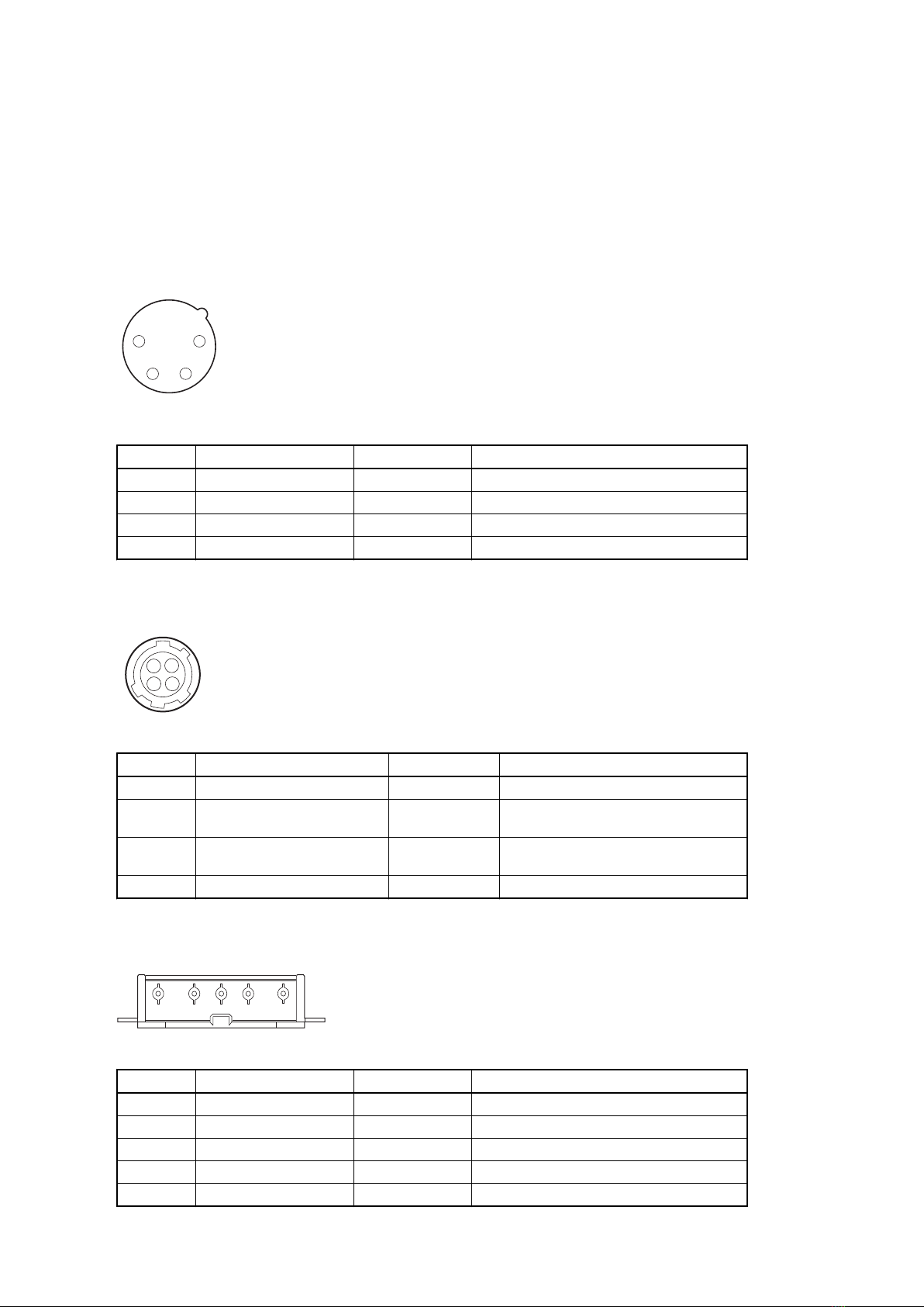
1-1. Connectors and Cables ....................................................................................................... 1-1
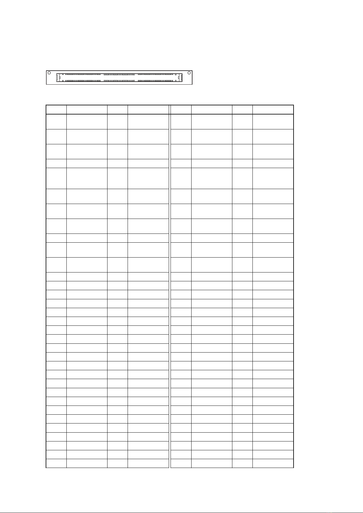
1-1-1. Connector Input/Output Signals........................................................................................1-1
1-1-2. Applicable Connector...................................................................................................1-4
1-2. Location of Main Parts........................................................................................................1-5
1-2-1. Location of Boards and Functions......................................................................................1-5
1-3. Functions of Onboard Switches and LED Indicators......................................................................... 1-6
1-3-1. DC-181 Board.......................................................................................................... 1-6
1-3-2. RE-340 Board...........................................................................................................1-6
1-3-3. SW-1706 Board.........................................................................................................1-7
1-3-4. SW-1714 Board.........................................................................................................1-7
1-4. Circuit Description............................................................................................................ 1-8
1-4-1. Board Configuration....................................................................................................1-8
1-4-2. Flow of Main Signals................................................................................................. 1-10
1-4-3. Power Control System.................................................................................................1-10
1-5. Notes on Replacement of Circuit Board.....................................................................................1-13
1-5-1. DM-157 Board........................................................................................................ 1-13
1-6. Updating Firmware Version..................................................................................................1-14
1-7. Acquiring Log Data..........................................................................................................1-15
1-8. Periodic Maintenance and Inspection........................................................................................1-16
1-8-1. Periodic Replacement Parts........................................................................................... 1-16
1-8-2. Cleaning of DC Fan...................................................................................................1-16
1-9. Circuit Protection Parts...................................................................................................... 1-17
1-9-1. Circuit Protection Element............................................................................................1-17
1-9-2. Replacing Fuses.......................................................................................................1-17
1-10. Service Tools.................................................................................................................1-18
1-11. Disconnecting/Connecting Fine-Wire Coaxial Cable........................................................................1-19
1-12. Lead-free Solder............................................................................................................. 1-20
1-13. Forming Harness Guard PS..................................................................................................1-21
2. Replacement of Main Parts
2-1. Tightening Torque.............................................................................................................2-1
2-2. Docking Module...............................................................................................................2-2
2-3. Battery Harness................................................................................................................2-3
2-4. Rear Case Assembly.......................................................................................................... 2-5
2-5. DC Fan........................................................................................................................ 2-7
2-6. RE-IF-Power Harness (Disconnecting from the Connector)..................................................................2-8
2-7. RE-340 Board, DD-49 Board................................................................................................. 2-9
2-8. SW-1706 Board..............................................................................................................2-12
2-9. Duct Assembly...............................................................................................................2-13
2-10. Slot Assembly................................................................................................................2-15
2-11. SCN-17 Board............................................................................................................... 2-17
AXS-R7 1

2-12. DM-157 Board...............................................................................................................2-19
2-13. IF-1318 Board................................................................................................................2-22
2-14. IF-1308 Board................................................................................................................2-26
2-15. DC-181 Board................................................................................................................2-32
2-16. DC OUT Connector..........................................................................................................2-34
2-17. DC IN Connector............................................................................................................ 2-35
2-18. SW-1714 Board..............................................................................................................2-37
2-19. SW Cover (Assign).......................................................................................................... 2-38
3. Spare Parts
3-1. Note on Repair Parts.......................................................................................................... 3-1
3-2. Exploded Views............................................................................................................... 3-2
Inside Panel ..........................................................................................................................3-2
Rear Case Block..................................................................................................................... 3-3
Main Duct Block.....................................................................................................................3-4
Slot Assembly........................................................................................................................3-5
Front Panel Block....................................................................................................................3-6
Docking Module..................................................................................................................... 3-7
3-3. Supplied Accessories .........................................................................................................3-8
4. Diagrams
Overall..................................................................................................................................4-1
Frame Wiring...........................................................................................................................4-2
Revision History
AXS-R7 2

Manual Structure
Purpose of this manual
This manual describes the maintenance and block service of this unit. The contents are written for system engineers and
service engineers with special knowledge.
Related manuals
• Service Manual
This manual describes the information for block service of this unit.
• Factory Service Manual
This manual describes the information for component service of this unit. This manual is required to repair the
mounted circuit board by replacing parts.
AXS-R7 3


Section 1
Service Overview
1-1. Connectors and Cables
1-1-1. Connector Input/Output Signals
1. DC IN
1
23
4
- External View -
XLR 4-pin, Male
No. Signal I/O Specifications
1 GND — GND for DC (+)
2 — — No connection
3 — — No connection
4 DC (+) IN 11 V to 17 V, DC
2. DC OUT 12 V
1
23
4
- External View -
4-pin, Female
No. Signal I/O Specification
1 UNREG_GND — GND for POWER
2 REC_TALLY OUT Open Collector output (Max. 50 mA)
Low : REC
3 REC_TRIGGER IN Open or +2.5 V, DC: No Operation
GND: Active (REC)
4 UNREG_+12 V OUT 11 V to 17 V, DC
3. BATT IN
12345
- External View -
5-pin, Male
No. Signal I/O Specifications
1 BATT IN (–) IN GND
2 BATT ID IN Battery identification
3 BATT SDA IN/OUT Serial data
4 BATT SCL OUT Clock
5 BATT IN (+) IN 11 V to 17 V, DC
AXS-R7 1-1

4. Camera mount
- External View -
152-pin, Female
143 146
147144
149
150
152 151
1
2
148 145
No. Signal I/O Specifications No. Signal I/O Specifications
1 ADAPTOR_
DET0_X
OUT — 2 ADAPTOR_
DET2_X
IN GND
3 ADAPTOR_
TYPEID#0
OUT GND 4 ADAPTOR_
TYPEID#1
OUT GND
5 ADAPTOR_
TYPEID#2
OUT OPEN 6 ADAPTOR_
TYPEID#3
OUT OPEN
7 BATTERY_ID#0 OUT GND 8 BATTERY_ID#1 OUT GND
9 (IF)2(EXT)_
ADAPTOR_
READY
OUT — 10 (IF)2(EXT)_
EXT_INT_X
OUT —
11 (EXT)2(IF)_
POWER_GOOD
IN — 12 GND — GND
13 (EXT)2(IF)_
POWER_ON
IN — 14 (EXT)2(IF)_
BATT_SDA
IN —
15 BATT_ID IN — 16 (EXT)2(IF)_
BATT_SCL
IN —
17 GND — GND 18 GND — GND
19 (IF)2(EXT)_
REC_TRIGGER
IN — 20 (EXT)2(IF)_
UART_TX
IN —
21 (EXT)2(IF)_
REC_TALLY
OUT — 22 (IF)2(EXT)_
UART_RX
OUT —
23 GND — GND 24 GND — GND
25 — — NC 26 — — NC
27 — — NC 28 — — NC
29 — — NC 30 — — NC
31 GND — GND 32 GND — GND
33 — — NC 34 — — NC
35 — — NC 36 — — NC
37 GND — GND 38 GND — GND
39 — — NC 40 — — NC
41 — — NC 42 — — NC
43 GND — GND 44 GND — GND
45 — — NC 46 — — NC
47 — — NC 48 — — NC
49 GND — GND 50 GND — GND
51 GND — GND 52 GND — GND
53 — — NC 54 — — NC
55 — — NC 56 — — NC
57 — — NC 58 — — NC
59 — — NC 60 — — NC
61 — — NC 62 — — NC
63 GND — GND 64 — — NC
65 — — NC 66 — — NC
Continued
AXS-R7 1-2

No. Signal I/O Specifications No. Signal I/O Specifications
67 — — NC 68 — — NC
69 GND — GND 70 GND — GND
71 — — NC 72 — — NC
73 — — NC 74 — — NC
75 GND — GND 76 GND — GND
77 — — NC 78 — — NC
79 — — NC 80 — — NC
81 GND — GND 82 GND — GND
83 — — NC 84 — — NC
85 — — NC 86 — — NC
87 GND — GND 88 GND GND
89 — — NC 90 — — NC
91 — — NC 92 — — NC
93 GND — GND 94 GND — GND
95 GND — GND 96 GND — GND
97 (EXT)2(IF)_
GOLGO_TX3_P
IN — 98 (IF)2(EXT)_
GOLGO_RX3_P
OUT —
99 (EXT)2(IF)_
GOLGO_TX3_N
IN — 100 (IF)2(EXT)_
GOLGO_RX3_
N
OUT —
101 GND — GND 102 GND — GND
103 (EXT)2(IF)_
GOLGO_TX2_P
IN — 104 (IF)2(EXT)_
GOLGO_RX2_P
OUT —
105 (EXT)2(IF)_
GOLGO_TX2_N
IN — 106 (IF)2(EXT)_
GOLGO_RX2_
N
OUT —
107 GND — GND 108 GND — GND
109 (EXT)2(IF)_
GOLGO_TX1_P
IN — 110 (IF)2(EXT)_
GOLGO_RX1_P
OUT —
111 (EXT)2(IF)_
GOLGO_TX1_N
IN — 112 (IF)2(EXT)_
GOLGO_RX1_
N
OUT —
113 GND — GND 114 GND GND
115 (EXT)2(IF)_
GOLGO_TX0_P
IN — 116 (IF)2(EXT)_
GOLGO_RX0_P
OUT —
117 (EXT)2(IF)_
GOLGO_TX0_N
IN — 118 (IF)2(EXT)_
GOLGO_RX0_
N
OUT —
119 GND — GND 120 GND — GND
121 — — NC 122 — — NC
123 — — NC 124 — — NC
125 GND — GND 126 GND — GND
127 — — NC 128 — — NC
129 — — NC 130 — — NC
131 GND — GND 132 GND — GND
133 — — NC 134 — — NC
135 — — NC 136 GND — GND
137 GND — GND 138 — — NC
139 — — NC 140 — — NC
141 GND — GND 142 GND GND
Continued
AXS-R7 1-3

No. Signal I/O Specifications No. Signal I/O Specifications
143 BODY_DE-
TECT
IN — 144 ADAPTOR_
DET1_X
OUT —
No. Signal I/O Specifications No. Signal I/O Specifications
145 BATTERY(+) OUT 11 V to 17 V 148 EXT_DC(+) OUT 11 V to 17 V
146 BATTERY(+) OUT 11 V to 17 V 149 EXT_DC(+) OUT 11 V to 17 V
147 BATTERY(+) OUT 11 V to 17 V 150 EXT_DC(+) OUT 11 V to 17 V
151 BATTERY(–) OUT GND for BAT-
TERY
152 EXT_DC(–) OUT GND for EXT_
DC
1-1-2. Applicable Connector
The connectors applicable to the terminal of the unit are as follows.
Panel Indication Connector Name Applicable Connector Part No.
DC IN XLR 4P, Female —
DC OUT Round Type 4P, Male 1-566-425-11
AXS-R7 1-4

1-2. Location of Main Parts
1-2-1. Location of Boards and Functions
DD-49 SW-1714
DM-157
RE-340 DC-181
IF-1308
IF-1318
SW-1706
SCN-17
Location Board name Function
Main unit DD-49 Power supply
DM-157 RAW codec
IF-1318 Camera interface
RE-340 Power control system
SCN-17 Memory card interface
SW-1706 Slot select switch and indicator
Docking module DC-181 DC IN/OUT, camera interface
IF-1308 Camera interface extension
SW-1714 PB select switch and indicator
AXS-R7 1-5

1-3. Functions of Onboard Switches and LED Indicators
1-3-1. DC-181 Board
S302
DC-181 board (Side A)
Ref. No. (address) Color Description Normal state
S302 (B-3) — Version update button —
1-3-2. RE-340 Board
D204D206
RE-340 board (Side A)
AXS-R7 1-6

Ref. No. (address) Color Description Normal state
D204 (—) Red TALLY lamp
Lights during recording
Blinks when an abnormality to be handled as an error or warning
occurs.
<Main cause>
Flashing (1 time/sec): Remaining media warning (about 5 mi-
nutes)
Flashing (4 times/sec): No remaining media or an error occurred
Tip
For other causes, refer to the operating instructions for the con-
nected camcorder.
Off
D206 (—) Green POWER indicator
Lights when power is supplied from the camcorder.
Lights
1-3-3. SW-1706 Board
D201
D202
S101
SW-1706 board (Side A)
Ref. No. (address) Color Description Normal state
S101 (—) — SLOT SELECT button —
D201 (—) Red/Green ACCESS lamp A
Indicates the status of card slot A.
Red: The mounted AXS-A memory card is being accessed.
Green: Standby state (Recording and playback are enabled by
using the mounted AXS-A memory card.)
Off: When a valid memory card is not inserted
Off
D202 (—) Red/Green ACCESS lamp B
Indicates the status of card slot B.
Red: The mounted AXS-A memory card is being accessed.
Green: Standby state (Recording and playback are enabled by
using the mounted AXS-A memory card.)
Off: When a valid memory card is not inserted
Off
1-3-4. SW-1714 Board
S100
D100
SW-1714 board (Side A)
Ref. No. (address) Color Description Normal state
S100 (—) — PLAYBACK SELECT button —
D100 (—) Green PLAYBACK SELECT indicator
Lights when playback of data is possible.
Lights
AXS-R7 1-7

1-4. Circuit Description
1-4-1. Board Configuration
This unit consists of the following boards.
• DM-157 board: Processes video and audio signals and controls the system.
• RE-340 board: Controls power.
• DD-49 board: Generates power voltages to be supplied to each board.
• SCN-17 board (two boards): Connects an AXS-A memory card.
• SW-1706 board: Contains the SLOT SELECT button and ACCESS lamps A and B.
• IF-1318 board: Relays video/audio/control signals and power.
• DC-181 board: Contains the version update button, relays video and audio signals, and connects the DC IN and
DC-OUT connectors.
• IF-1308 board: Connects a camcorder and other devices.
• SW-1714 board: Contains the PLAYBACK SELECT button and indicators.
DM-157 Board
The DM-157 board mainly consists of the system controller CPU (IC2900: Diablo) and the data processor FPGA
(IC0100).
Video and audio signals from the extended interface connector on the IF-1308 board are sent to the FPGA (IC0100)
through the Equalizer/Driver IC (IC0500).
The FPGA (IC0100) has a function of interface between the AXS memory card connected to the two SCN-17 boards.
Furthermore, four 1G x 8bit DDR3L SDRAM cards are connected to the FPGA (IC0100) as the main cache.
FPGA (IC0100) configuration data is stored in the 256M SPI flash memory. Two SPI flash memory cards are mounted
to switch configuration of the FPGA (IC0100) according to functions.
Two 128M x 16bit DDR2 SDRAM cards are connected to the CPU (IC2900) as the main memory, and two 128Mbit
SPI Flash memory cards are mirrored as the boot ROM.
One lane of PCI Express Gen1 is connected between the CPU (IC2900) and the FPGA (IC0100), which is used for main
communication between these ICs. Synchronization between these two ICs is ensured by sending the VSYNC signal
from the FPGA (IC0100) to the CPU (IC2900).
RE-340 Board
The RE-340 board controls entire power of the unit. DC IN power or battery power is selected as power input to the
unit.
The RE-340 board generates single-channel +2.5 V and supplies it to each board.
The RE-340 board contains the power control IC CPLD (IC107) to drive the cooling fan, POWER indicator, and TALLY
lamp. This board also controls power of the SCN-17 board.
DD-49 Board
The DD-49 board generates three-channel +3.3 V and single-channel +5 V from the power supplied from the RE-340
board and supplies these voltages to each board.
AXS-R7 1-8

SCN-17 Board
The SCN-17 board contains the AXS-A memory connector (CN100). The data line of the AXS-A memory connector
and the EXIST signal to recognize installation of AXS-A memory card are sent from CN103 to the FPGA (IC0100) on
the DM-157 board. The EXIST signal is also connected to the RE-340 board from CN102 to control power.
Two SCN-17 boards are used in AXS-R7 because two AXS-A media slots are provided.
SW-1706 Board
The SW-1706 board contains the SLOT SELECT button, ACCESS lamp A, and ACCESS lamp B.
The SLOT SELECT button is connected to the CPU (IC2900) on the DM-157 board.
Control signals of ACCESS lamp A and ACCESS lamp B are connected to the FPGA (IC0100) on the DM-157 board.
IF-1318 Board
The IF-1318 board relays control signals (including video/audio signals, RS-232C signals, and version update signal)
between DC-181 board and DM-157 board.
The IF-1318 board is connected to the DC-181 board through CN100.
Video and audio signals from the camcorder are connected from CN101 to the FPGA (IC0100) on the DM-157 board.
Signals for the camcorder to recognize or control this unit are connected from CN102 to the DM-157 board.
The PLAYBACK SELECT button signal and the PLAYBACK SELECT indicator signal from the SW-1714 board and
the version update button signal from the DC-181 board are connected from CN103 to the CPU (IC2900) on the DM-157
board.
Furthermore, power lines are connected from CN105 (Battery power), CN106 (GND), and CN107 (DC IN power) to
the RE-340 board.
DC-181 Board
The DC-181 board relays control signals (including video/audio signals and RS-232C signals) between IF-1301 board
and IF-131 board.
The DC-181 board is connected to the IF-1318 board through CN100.
The DC-181 board contains the DC IN power input connector (CN202) and the DC OUT connectors (CN204/CN205).
This board selects DC IN power or battery power as DC OUT power, and outputs the selected power.
Furthermore, the DC-181 board contains the version update button and the version update connector. The version update
button signal is connected to the CPU (IC2900) on the DM-157 board and the CPLD (IC107) on the RE-340 board
through the IF-1318 board.
IF-1308 Board
The IF-1308 board contains an extended interface connector for connection to a camcorder.
Extended interface video/audio signals are connected from CN102 through the DC-181 and IF-1318 boards to the
DM-157 board. Signals for the camcorder to recognize or control this unit are connected from CN101 through the
DC-181 and IF-1318 boards to the DM-157 board.
The CN IN/Battery power lines are connected from CN103 through the DC-181 and IF-1318 boards to the RE-340
board.
AXS-R7 1-9

SW-1714 Board
The SW-1714 board contains the PLAYBACK SELECT button and the PLAYBACK SELECT indicator. Signals of this
button and this indicator are connected to the CPU (IC2900) on the DM-157 board through the DC-181 and IF-1318
boards.
1-4-2. Flow of Main Signals
Recording video/audio signals
Video and audio signals from the camcorder are input to this unit from the extended interface connector on the IF-1308
board. These signals are sent through the IF-1318 board and the Equalizer/Driver IC (IC500) on the DM-157 board to
the FPGA (IC0100).
The FPGA (IC0100) separates video data, audio data, and meta data and compresses only video data. Compressed video
data, audio data, and meta data are individually packetized and are then recorded in the AXS-A memory card connected
to the SCN-17 board. At this time, the four DDR3L SDRAM cards connected to the FPGA (IC0100) are used as data
buffers for data separation and packetization.
In the playback mode, data that is read from the AXS-A memory card connected to the selected SCN-17 board is decoded
in the FPGA (IC0100). Video and audio signals (including video data, audio data, and meta data) are sent to the Equalizer/
Driver IC (IC0500) on the DM-157 board, IF-1318 board, and DC-181 board, and are then sent from the extended
interface connector on the IF-1308 board to the camcorder.
Playback images can be monitored as camcorder’s output images.
Mounting the memory card
When an AXS-A memory card is inserted, the EXIST signal of the SCN-17 board turn low from open. This low-level
signal is sent to the FPGA (IC0100) on the DM-157 board and the RE-340 board, which allows this unit to recognize
that an AXS-A memory card has been mounted and supply power to the AXS-A memory card.
Version Update
The version update button (located in the panel secured with screws at the bottom of the unit) on the DC-181 board
allows users to update versions. When the version update button is pressed, control signals are sent from the DC-181
board through the IF-1318 board to the CPU (IC2900) on the DM-157 board and the CPLD (IC107) on the RE-340
board. Then the CPU (IC2900) and the CPLD (IC107) recognize that the version update button is being pressed.
The data that is read from the storage medium inserted into the version update connector on the DC-181 board is sent
from the DC-181 board through the IF-1318 board and the controller (IC1901) on the DM-157 board to the CPU
(IC2900).
1-4-3. Power Control System
Input power
Power is supplied to the unit by selecting DC IN power or battery power as power input. When both of these are
connected, DC IN power is selected. The selected voltage is referred to as “SW_UNREG” hereafter.
• Input overcurrent protection of DC IN
A 15A fuse (F201) on the DC-181 board is installed at the DC IN input end for overcurrent protection.
AXS-R7 1-10

• Input inverse-voltage protection of DC IN
When DC IN is an inverse voltage, the FET (Q205) on the DC-181 board does not work to prevent the inverse
voltage from being supplied to boards.
• Overcurrent protection of SW_UNREG
The input voltage SW_UNREG is protected by the overcurrent detection circuit (IC108) on the RE-340 board.
When a current larger than approx. 9 A flows in the SW_UNREG line, the SW_UNREG voltage is shut off. Since
the overcurrent detection circuit is not reset automatically even after the overcurrent is cleared, the unit must be
powered on again.
• Low-voltage protection and overvoltage protection of SW_UNREG
The input voltage SW_UNREG is protected by the low-voltage detection circuit and the overvoltage detection
circuit (IC101) on the RE-340 board.
Low-voltage protection circuit: SW_UNREG is turned on at approx. 8.7 V or more and is shut off at approx.
Overvoltage protection circuit: SW_UNREG is turned on at approx. 18.0 V or less and is shut off at approx. 18.9
V.
These circuits do not stop by latching when SW_UNREG is shut off and work automatically when normal voltage
is restored
Overcurrent protection of the DC OUT connector
The input voltage SW_UNREG can be supplied from the DC OUT connector to external devices.
The DC OUT line is protected by the overcurrent detection circuit (IC201). When a current larger than approx. 2.4 A
flows in the DC OUT line, the DC OUT line is shut off. Since power is not restored automatically even the overcurrent
is cleared, the unit must be powered on again.
Voltage conversion
The input voltage SW_UNREG is converted by the DC-DC converter to generate voltages +3.3 V_1, +3.3 V_4 (IC101),
+5.0 V, and +3.3 V_2 (IC102) in the DD-49 board and also generate a voltage of +2.5 V (IC201) in the RE-340 board.
Overcurrent protection in each power channel
If any voltage (+2.5 V, +3.3 V-1, +3.3 V-2, +3.3 V-3, +3.3 V-4, or +5.0 V) is shut off by overcurrent protection of each
DC-DC converter, only the DC-DC converter in which overcurrent was generated is deactivated.
Since power is not restored automatically even the overcurrent is cleared, the unit must be powered on again.
Power driving sequence
Since no power switch is provided in the unit, power is controlled from the camcorder. When power is turned on in the
camcorder, the POWER_GOOD signal is sent to the RE-340 board and the SW_UNREG signal is output. Then a voltage
of +3.3 V_DC is generated by the regulator and the RE-340 board controller CPLD (IC107) is activated.
Furthermore, the POWER_ON signal is sent to the RE-340 board. When the CPLD (IC107) on the RE-340 board senses
this signal, the DC-DC converter (IC101, IC102) on the DD-49 board and the DC-DC converter (IC201) on the RE-340
board are activated and these converters supply voltages +5.0 V, +3.3 V_1, +3.3 V_2, and +2.5 V to the DM-157 board.
When the DM-157 board can correctly generate power voltages for each IC from +5.0 V, +3.3 V_1, +3.3 V_2, and +2.5
V, the LP_PGOOD signal is sent to the FET (Q201) on the DD-49 board. The DC-DC converter IC103 generates +2.5
V and sends the Power Good signal to IC101. The FET (Q201) on the DD-49 board generates +3.3 V_3 from +3.3V_
2 generated by the DC-DC converter (IC102) and sends the RE_PGOOD signal to the CPLD (IC107) on the RE-340
board.
AXS-R7 1-11

Cooling fan control
The cooling fan is controlled by the RE-340 board. The voltage of the fans is approx. 4.5 V to 12 V.
The set voltage value is supplied as a PWM signal from the FPGA (IC100) on the DM-157 board, and is then sent to
the CPLD (IC107) on the RE-340 board.
The CPLD (IC107) on the RE-340 board monitors the fan rotating status and sends the PWM signal to the fan driver
(IC202 and IC103) on the DD-49 board to generate a fan voltage.
LED control
The following LEDs are controlled by the CPLD (IC107) on the RE-340 board.
• POWER indicator
• TALLY lamp
AXS-R7 1-12
Other manuals for AXS-R7
3
Table of contents
Other Sony Measuring Instrument manuals

Sony
Sony PCM-D100 User manual

Sony
Sony MDX-C800REC User manual

Sony
Sony FDDR-7000 User manual

Sony
Sony RDR-VX500 (RDRVX500) User manual

Sony
Sony PWS-100TD1 User manual

Sony
Sony PCM-D100 Reference guide

Sony
Sony MZ-N920 User manual

Sony
Sony DG805BLM User manual

Sony
Sony MAVE-F555 User manual

Sony
Sony MG40 Series Installation manual