Texas Instruments ADS5231 EVM User manual
Other Texas Instruments Control Unit manuals
Texas Instruments
Texas Instruments DS160PR412-421EVM User manual
Texas Instruments
Texas Instruments WL1835MODCOM8B User manual
Texas Instruments
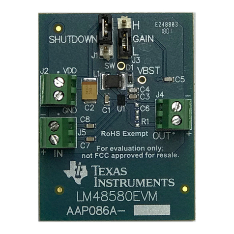
Texas Instruments LM48580 User manual
Texas Instruments
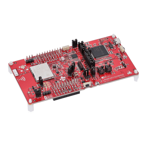
Texas Instruments SimpleLink CC3235MODS User manual
Texas Instruments
Texas Instruments TPS61020EVM User manual
Texas Instruments
Texas Instruments ADS1254 User manual
Texas Instruments
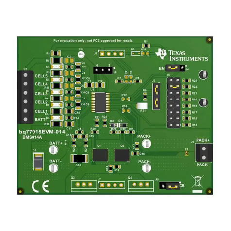
Texas Instruments bq77915EVM-014 User manual
Texas Instruments
Texas Instruments 990 User manual
Texas Instruments
Texas Instruments THS3061EVM User manual
Texas Instruments
Texas Instruments TPS6101xEVM-157 User manual
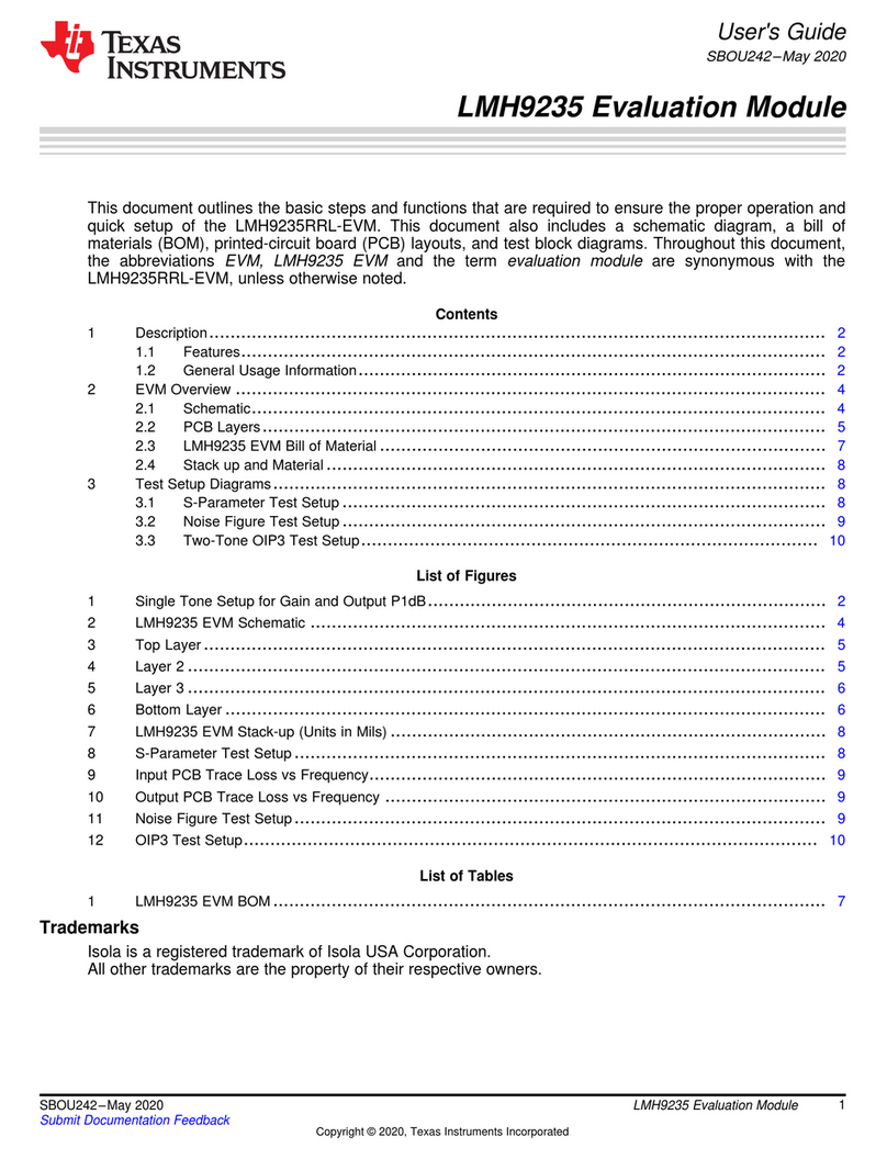
Texas Instruments
Texas Instruments LMH9235RRL-EVM User manual
Texas Instruments
Texas Instruments OPT8241-CDK-EVM User manual
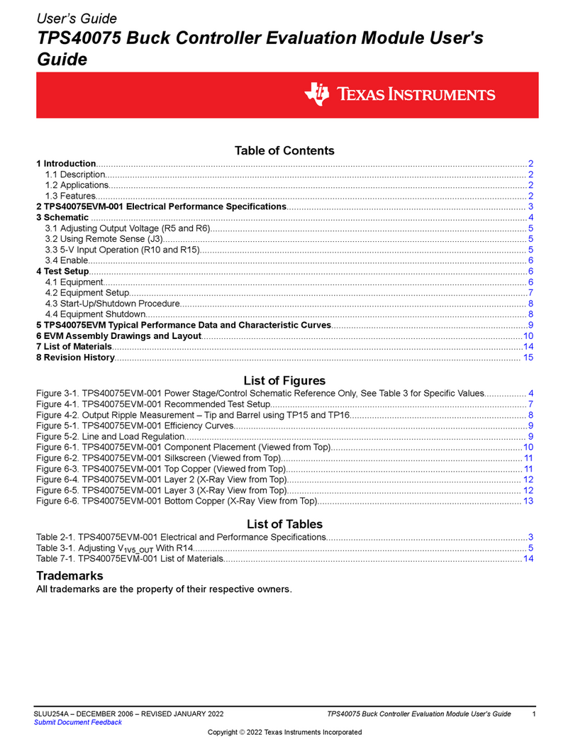
Texas Instruments
Texas Instruments TPS40075EVM-001 User manual
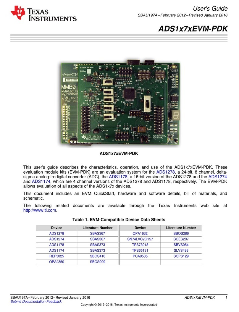
Texas Instruments
Texas Instruments ADS1x7xEVM-PDK User manual
Texas Instruments
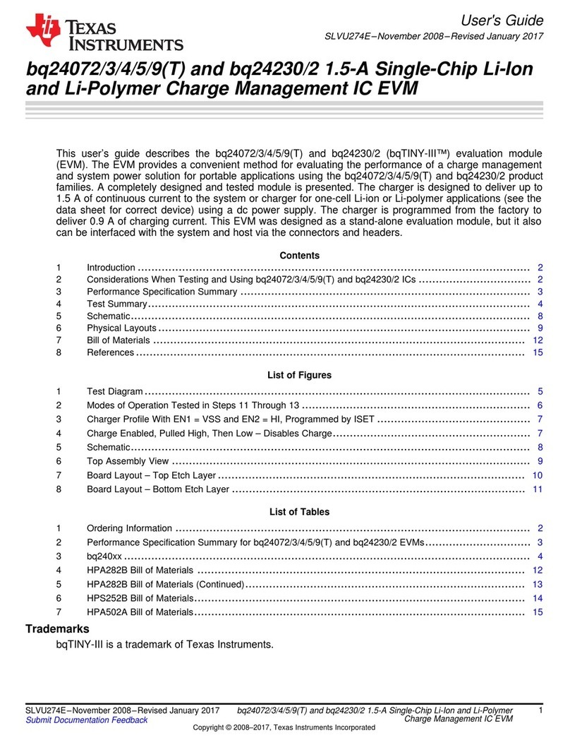
Texas Instruments bq24072 User manual
Texas Instruments
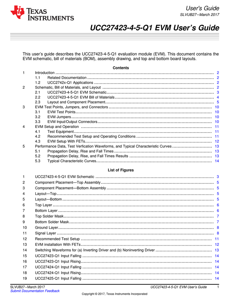
Texas Instruments UCC27423-Q1 User manual
Texas Instruments
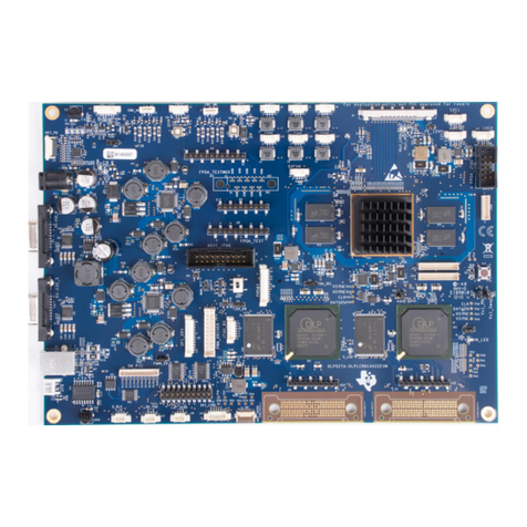
Texas Instruments DLPDLCR660TEVM User manual
Texas Instruments
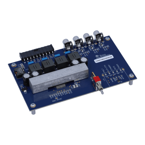
Texas Instruments TAS5514B User manual
Texas Instruments
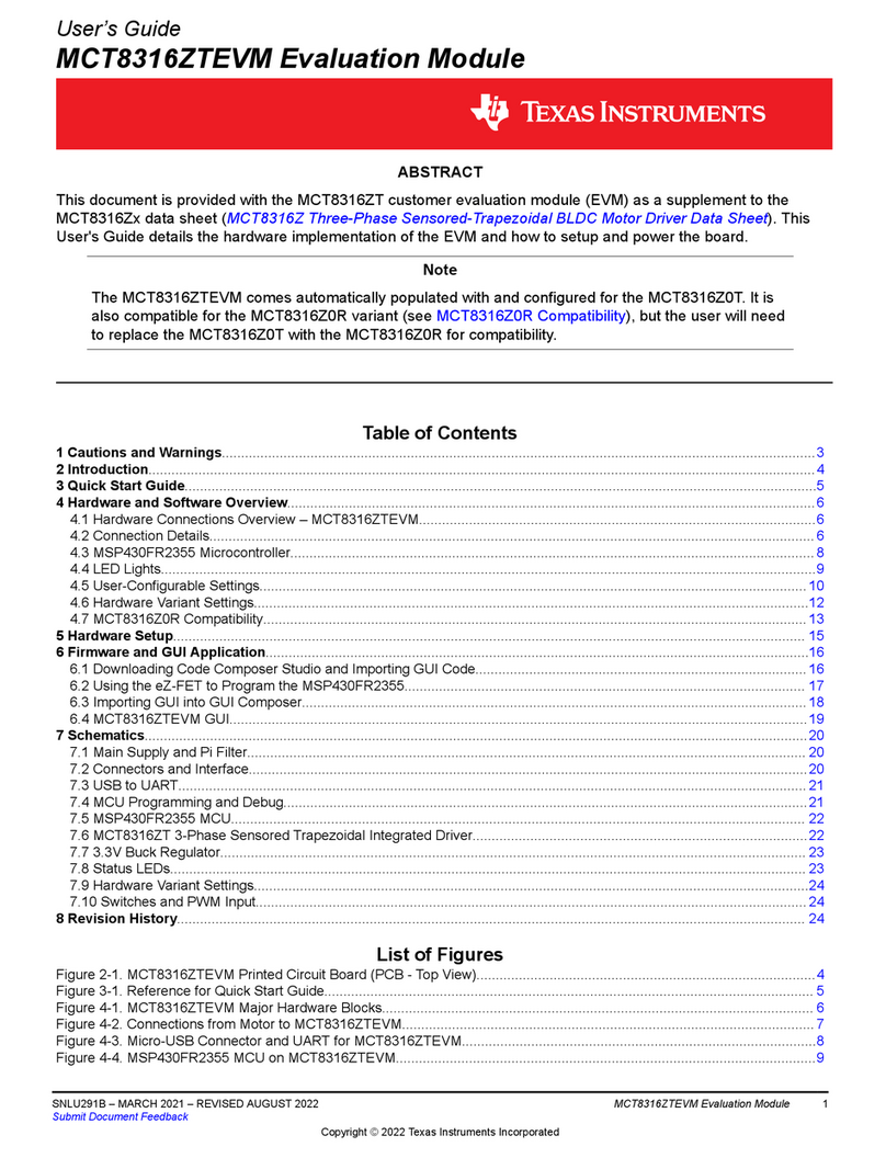
Texas Instruments MCT8316ZTEVM User manual
Texas Instruments
Texas Instruments TLC694 Series Product manual
Popular Control Unit manuals by other brands
Festo
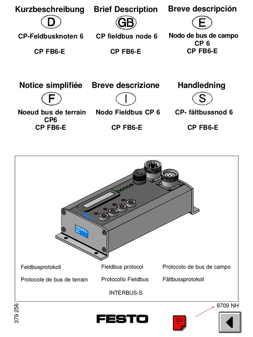
Festo Compact Performance CP-FB6-E Brief description
Elo TouchSystems
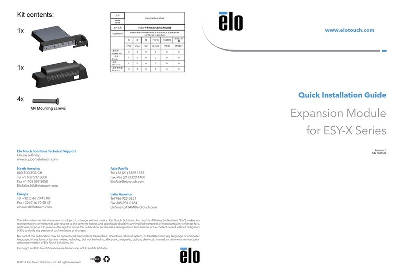
Elo TouchSystems DMS-SA19P-EXTME Quick installation guide
JS Automation
JS Automation MPC3034A user manual
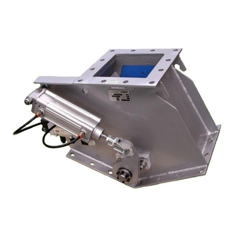
JAUDT
JAUDT SW GII 6406 Series Translation of the original operating instructions
Spektrum
Spektrum Air Module System manual
BOC Edwards
BOC Edwards Q Series instruction manual

KHADAS
KHADAS BT Magic quick start
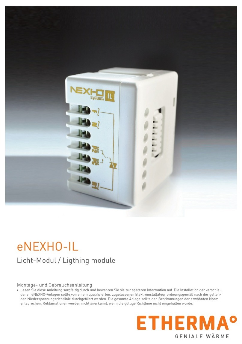
Etherma
Etherma eNEXHO-IL Assembly and operating instructions
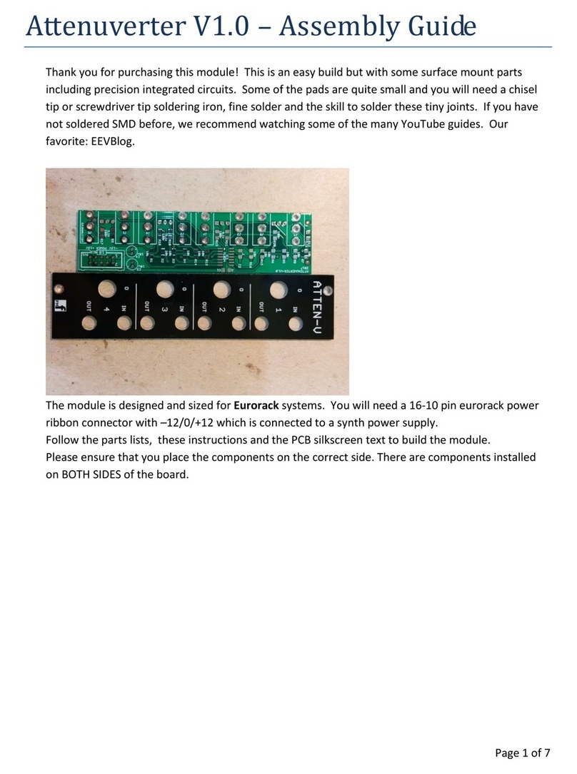
PMFoundations
PMFoundations Attenuverter Assembly guide
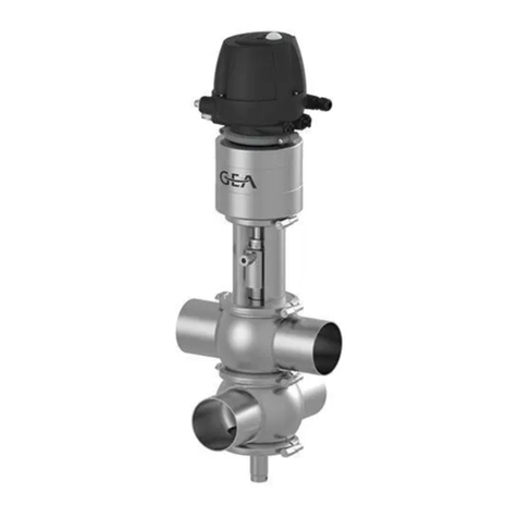
GEA
GEA VARIVENT Operating instruction
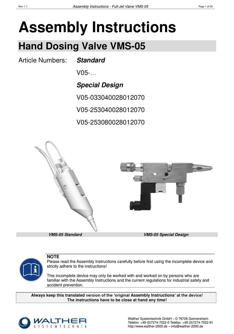
Walther Systemtechnik
Walther Systemtechnik VMS-05 Assembly instructions
Altronix
Altronix LINQ8PD Installation and programming manual
