Texas Instruments AN-2166 LMZ10500 User manual
Other Texas Instruments Control Unit manuals

Texas Instruments
Texas Instruments BOOSTXL-TPS652170 User manual
Texas Instruments
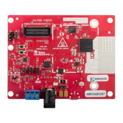
Texas Instruments AWR1642 User manual
Texas Instruments
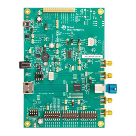
Texas Instruments DS90UB949A-Q1EVM User manual
Texas Instruments
Texas Instruments WL1835MODCOM8B User manual
Texas Instruments
Texas Instruments LMK00725EVM User manual
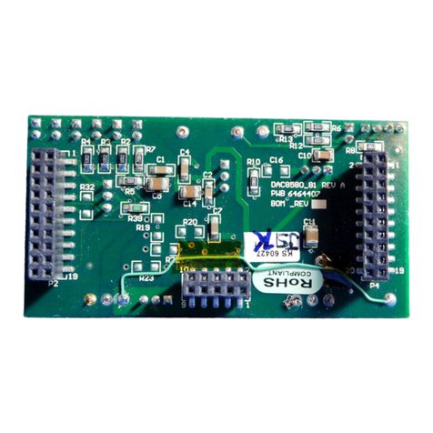
Texas Instruments
Texas Instruments DAC8580 User manual

Texas Instruments
Texas Instruments DAC7571 User manual
Texas Instruments
Texas Instruments FPD23DAEVM User manual
Texas Instruments
Texas Instruments TPA0142 User manual
Texas Instruments
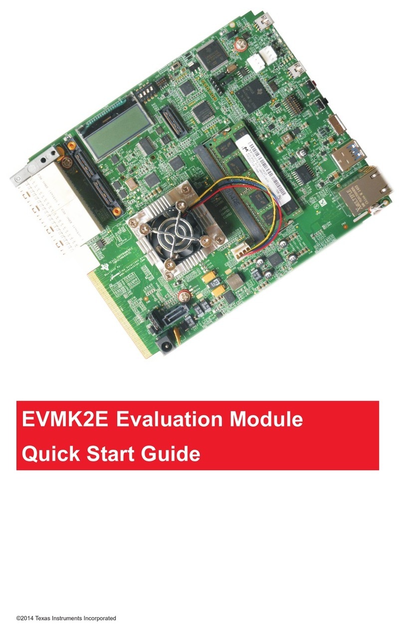
Texas Instruments EVMK2E User manual
Texas Instruments
Texas Instruments LMH9235RRL-EVM User manual
Texas Instruments
Texas Instruments UCC25600EVM User manual
Texas Instruments
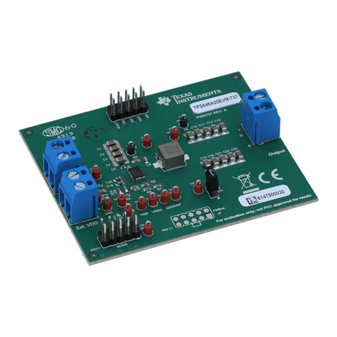
Texas Instruments SWIFT TPS548A20 User manual
Texas Instruments
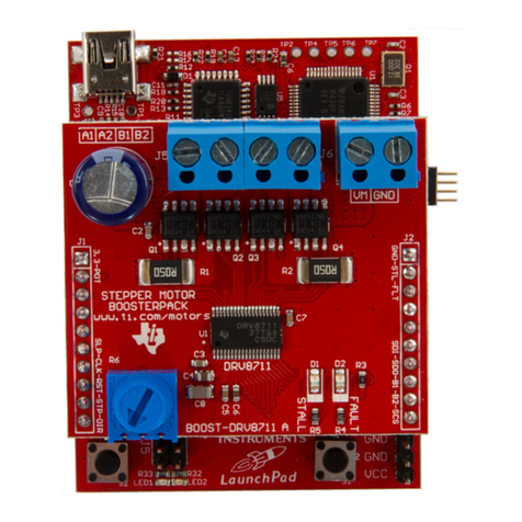
Texas Instruments BOOST-DRV8711 User manual
Texas Instruments
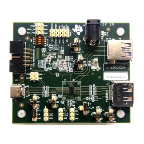
Texas Instruments TUSB564RNQ User manual
Texas Instruments
Texas Instruments TPS54672EVM-222 User manual
Texas Instruments
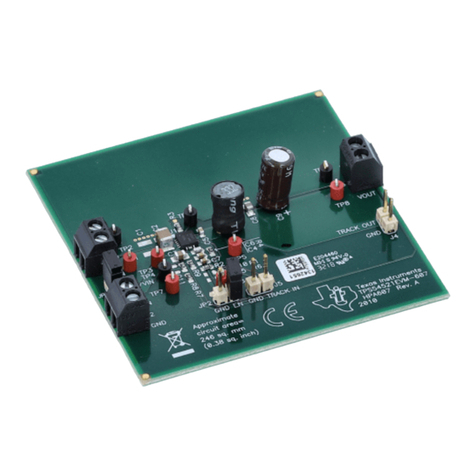
Texas Instruments TPS54521EVM-607 User manual
Texas Instruments
Texas Instruments TRF7962A User manual

Texas Instruments
Texas Instruments TPS53313 User manual
Texas Instruments
Texas Instruments UCC28740EVM-525 User manual
Popular Control Unit manuals by other brands
Festo
Festo Compact Performance CP-FB6-E Brief description
Elo TouchSystems
Elo TouchSystems DMS-SA19P-EXTME Quick installation guide
JS Automation
JS Automation MPC3034A user manual
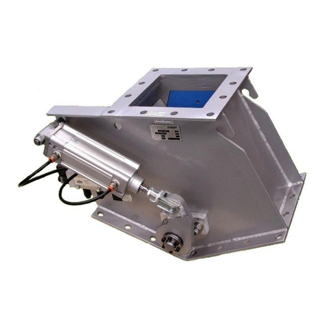
JAUDT
JAUDT SW GII 6406 Series Translation of the original operating instructions
Spektrum
Spektrum Air Module System manual
BOC Edwards
BOC Edwards Q Series instruction manual

KHADAS
KHADAS BT Magic quick start
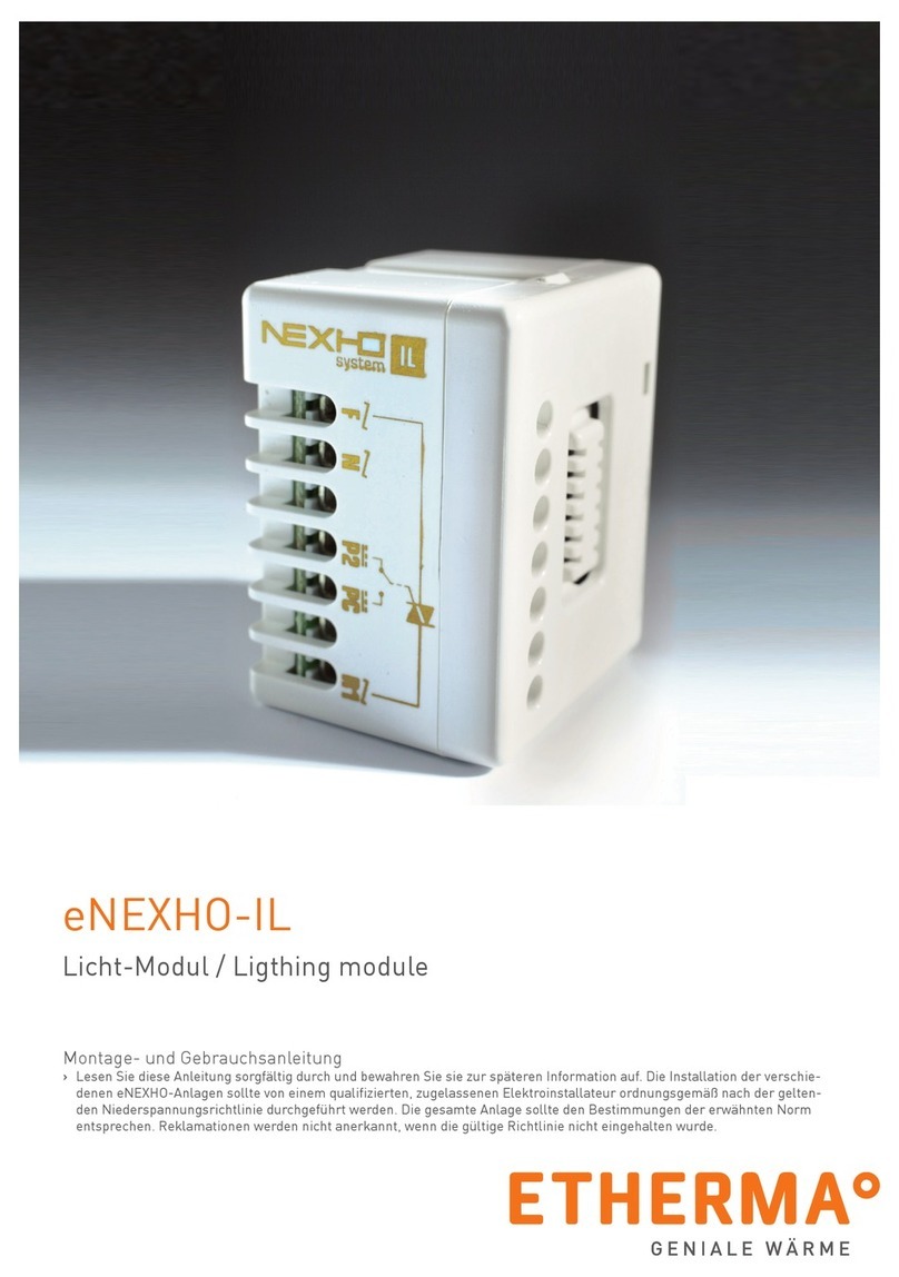
Etherma
Etherma eNEXHO-IL Assembly and operating instructions
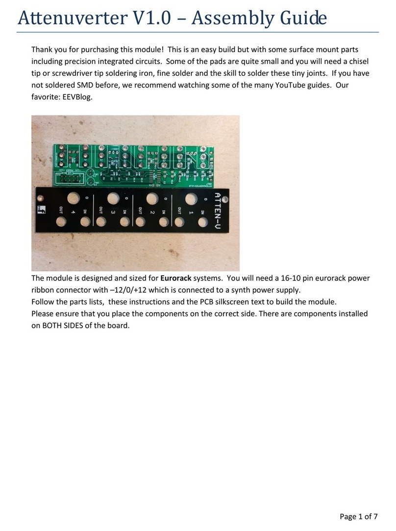
PMFoundations
PMFoundations Attenuverter Assembly guide
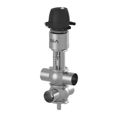
GEA
GEA VARIVENT Operating instruction
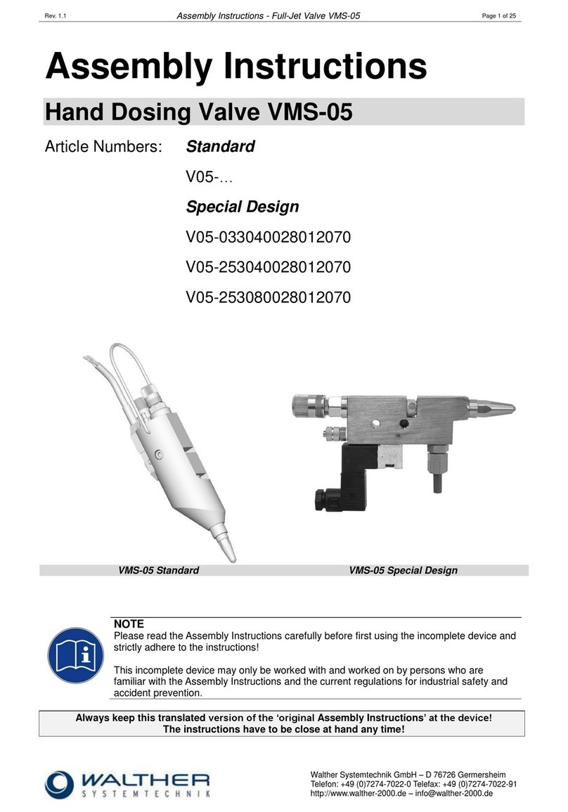
Walther Systemtechnik
Walther Systemtechnik VMS-05 Assembly instructions
Altronix
Altronix LINQ8PD Installation and programming manual
