Alinx AX7103 User manual

ALINX FPGA BOARD
AX7103
User Manual

AX7103 User Manual
2
/
Http://www.heijin.org
2 / 50
2 / 50
Revsion History:
Revision
Description
1.0
First Release

AX7103 User Manual
3
/
Http://www.heijin.org
3 / 50
3 / 50
Copyright Notice:
Copyright ©2018 byALINX Technologies inc. All rights are reserved.
Development Environment:
Vivado 2017.4 is from Xilinx website
https://www.xilinx.com
Official website:
Http://www.alinx.com.cn
E-mail:
Tel:
+86-021-67676997
WeChat public number:
ALINX-HEIJIN

AX7103 User Manual
4
/
Http://www.heijin.org
4 / 50
4 / 50
Contents
Overview............................................................................................................................5
FPGA Core Board ..............................................................................................................8
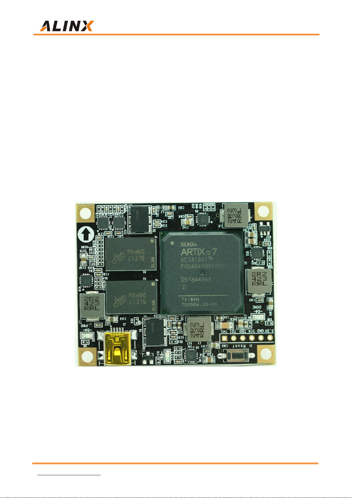
1. Overview................................................................................................................... 8
2. FPGA........................................................................................................................ 9
3. Differential Crystal Oscillator ................................................................................ 11
4. DDR3...................................................................................................................... 12
5. QSPI Flash.............................................................................................................. 16
6. LED light ................................................................................................................ 17
7. Reset Button............................................................................................................ 18
8. JTAG Interface........................................................................................................ 19
9. Power Input............................................................................................................. 19
10. Board-to-Board Connector ..................................................................................... 20
11. Power ...................................................................................................................... 27
12. Mechanical.............................................................................................................. 30
Expansion Board.............................................................................................................. 31
1. Preview ................................................................................................................... 31
2. Gigabit Ethernet...................................................................................................... 31
3. PCIe x4 Connector.................................................................................................. 33
4. HDMI Input Connector........................................................................................... 35
5. HDMI Input Connector........................................................................................... 37
6. SD socket................................................................................................................ 38
7. USB Serial Port....................................................................................................... 39
8. EEPROM 24LC04.................................................................................................. 41
9. GPIO Expansion Headers....................................................................................... 42
10. JTAG Connector ..................................................................................................... 45
11. XADC Connector(Not install by default)......................................................... 46
12. Buttons.................................................................................................................... 47
13. LED......................................................................................................................... 48
14. Power Supply.......................................................................................................... 49

AX7103 User Manual
5
/
Http://www.heijin.org
5 / 50
5 / 50
Overview
The ALINX ARTIX-7 FPGA Development board now released officially (module
number: AX7103). In order to learn the FPGA board quickly, we write this manual
for user.
The ARTIX-7 FPGAdevelopment platform includes core board and expansion board,
so that users can reuse the core board in their own projects conveniently. The kit
contains complete reference designs and source code for each part on board. It is a
good choice for students or FPGAengineers to learn Artix-7 FPGAand do evaluation
base on it. This document provides users key information about the kit. Figure1-1
shows a photograph of the whole board.
The AX7103 board comprised FPGA core board and expansion board, four
high-speed board-to-board connectors are used to connect between the core board
and the expansion board
The core board is a minimal system which mainly consists of FPGA chipset, two
DDR3 and QSPI FLASH. The expansion board extends many peripheral interfaces
for core board, which contains PCIex4 connector, gigabit Ethernet network port,
HDMI input, HDMI output, UART serial connector, SD socket, XADA connector, 2
pairs of 40-pin connector header and etc.
Below schematic diagram provides a quick overview of AX7103 board.

AX7103 User Manual
6
/
Http://www.heijin.org
6 / 50
6 / 50
LED*4
CP2102 USB
UART
PCIe x 4
KSZ9031
以太网
网口
按键*2
40针IO扩展口
SiI9134
HDMI
输出
XADC接
口
SD Card
JTAG
XILINX
ARTIX-7
FPGA
200Mhz
125Mhz
DDR3
DDR3
QSPI
FLASH
核心板
40针IO扩展口
KSZ9031
以太网
网口
SiI9013
HDMI
输入
Judge from the schematic diagram above, the AX7103 Development board could
achieve the below functions.
Artix-7 FPGA Core
The core board consists of XC7A100T+8Gb DDR3+128Mb QSPI FLAS, two high
resolution LVDS differential crystals of Sitime company, one is 200MHz used to
FPGASystem,another is 125MHz to provide stable clock input for GTPmodules.
PCIe x4 connector
Support PCI Express 2.0 standard,provide PCIe x4 High-speed data transmission
interface, single channel communication speed up to 5GBaud。
10/100M/1000M Ethernet RJ-45 connector
Gigabit Ethernet connector chip, that use KSZ9031RNX Ethernet PHY chip of
Micrel company, provide network communication services for user. Support
10/100/1000 Mbps network transmission rate; Full duplex and adaptive
HDMI Output
SIL9134 HDMI code chip of Silicon Image Company, support up to 1080P@60Hz
output,support 3D output。
HDMI Inupt
SIL9013 HDMI decode chip of Silion Image company,support up to 1080P@60Hz
input,and support date output in different format
USB Uart connector
One Uart transfer to USB connector,that used to communication with computer,
easy to debug. Serial chip USB-UAR of Silicon Labs CP2102GM, MINI USB
connector
Micro SD socket
One Micro SD socket,support SD mode and SPI mode
EEPROM
One chip EEPROM 24LC04 of IIC connector on board
2 pairs of 40-pin expansion header

AX7103 User Manual
7
/
Http://www.heijin.org
7 / 50
7 / 50
Reserved 2 pairs 2.54mm standard spacing 40-pin expansion header. They used to
connect all kinds of AXSOC modules or outside circuit designed by users. There are
40pins for every expansion header, and one pin for 5V power supply, 2 pins for 3.3V
power supply, 3 pins for ground, theother 34pins for IOs. Do not connected IOs to 5V
circuit directly, or may damage the FPGA, if to connect, that need through level
convert chip
JTAG Connector
10 pins 2.54mm standard JTAG Connectors, that use to download and debug the
FPGA program
2 Buttons
2 user Buttons (one button acts as reset button on core board)
LED Light
5 User LEDs and (one is on core board, four are on expansion board)

AX7103 User Manual
8
/
Http://www.heijin.org
8 / 50
8 / 50
FPGA Core Board
1. Overview
AC7100 (module number of Core Board) core board, is a high performance core
board using XILINX Artix-7 XC7A100T-2FGG484I chipset. Two DDR3 memories
are connected to FPGAwith 32bit data width and one 128Mbit QSPI FLASH is used
for storage of FPGA bitstreams or application code.
About 180 IOs (include 86 pairs LVDS signals) and signals of GTP transceivers
are extended to expansion board using board-on-board connector. The core board is
very small of 45*55 (mm), it will be a good choice to use this core board in project
which need a lot of IOs and space limitation
Figure 2-1-1 and Figure 2-1-2 shows the top view and bottom view of the FPGA
Core board.
AC7100 Top View

AX7103 User Manual
9
/
Http://www.heijin.org
9 / 50
9 / 50
AC7100 Bottom view
2. FPGA
AC7100 Core board uses Xilinx Artix-7 FPGAdevice, the detail part number is
XC7A100T-2FGG484I. Speed grade is 2, Temperature grade is industrial. The
Xilinx Artix-7 FPGA ordering information is shown in Figure 2-2-1.
Figure 2-2-1 Artix-7 Ordering Information

AX7103 User Manual
1
0
Http://www.heijin.org
10 / 50
10 / 50
Figure 2-2-1 FPGA chip
The feature summary of XC7A100T is listed as below
Items
Parameters
Logic Cells
101440
Slices
15850
CLB flip-flops
126800
Block RAM(kb)
4860
DSP Slices
240
PCIe Gen2
1
XADC
1 is 12bit, 1Mbps AD
GTP Transceiver
4,6.6Gb/s max
Speed grade
-2
Temperature Grade
Industrial
FPGA Power Supply
Artix-7 FPGA has six power supplies including VCCINT, VCCBRAM, VCCAUX, VCCO,
VMGTAVCC and VMGTAVTT. VCCINT is the core power supply of FPGAand should be
connected to +1.0V. VCCBRAM is power supply of FPGABlock RAM and also should
be connected to +1.0V. VCCAUX is FPGA auxiliary power supply and should be
connected to +1.8V. VCCO is each BANK power supply, because the IOs of FPGA
bank35 is connected to the DDR3, the VCCO voltage of bank35 should be +1.5V. VCCO
of Bank15 and Bank16 is power from a LDO chipset, so the voltage of these two
Bank can be changed if we use different LDO chipset. VMGTAVCC is the power supply
of GTP transceiver, it should be connected to +1.0V. VMGTAVTT is terminal power
supply of the GTP transceiver, and should be connected to the +1.2V
Artix-7 FPGA has the Power-On/Off Power supply sequencing, the
recommended power-on sequence is VCCINT, VCCBRAM, VCCAUX, and VCCO to achieve
minimum current draw and ensure that the I/Os are 3-stated at power-on. The

AX7103 User Manual
1
1
Http://www.heijin.org
11 / 50
11 / 50
recommended power-off sequence is the reverse of the power-on.
3. Differential Crystal Oscillator
AC7100 core board is equipped with two Sitime differential crystal oscillators ,
one is 200Mhz differential crystal oscillator for FPGA system clock, another is
148.5Mhz differential crystal oscillator for GTP transceiver reference.
1). 200Mhz Differential Crystal Oscillator
The Figure 2-3-1 is the circuit of 200Mhz system clock, the output of differential
crystal oscillator is connected to global clock pin MRCC (R4 and T4) of FPGA. The
200Mhz system clock can produce different frequency clock to drive the user logic
thought PLLs and DCMs inside FPGA.
Figure 2-3-1 200Mhz Differential Crystal Oscillator
Figure 2-3-2 is 200Mhz Differential Crystal Oscillator on board.
Figure 2-3-2 200Mhz Differential Crystal Oscillator
Pin Assignment of Clock:
Net Name
FPGA PIN
SYS_CLK_P
R4
SYS_CLK_N
T4

AX7103 User Manual
1
2
Http://www.heijin.org
12 / 50
12 / 50
2). 125Mhz Differential Clock
The differential crystal oscillator marked as G2 in Figure 2-3-3, used to provide
the reference input clock to GTPmodules in FPGA. The Figure 2-3-3 is the circuit of
125Mhz clock for GPT transceiver. The output of differential crystal oscillator is
connected to MGTREFCLK0P pin (F6) and MGTREFCLK0N pin (E6) of FPGA.
Figure 2-3-3 125Mhz Differential Crystal Oscillator
Figure 2-3-4 is 为125M Differential Active Crystal Oscillator
Figure2-3-4 125M Oscillator on board
Pin assignment of Clock:
Net Name
FPGA PIN
MGT_CLK0_P
F6
MGT_CLK0_N
E6
4. DDR3
The core board features 4GB of DDR3 memory, implemented using four
512MB DDR3 devices. The data bandwidth is in 32-bit, comprised of two x16
devices with a single address/command bus. The target clock speed for FPGA and
DDR3 is 800 MHz (Data rate is 1600M). The part number of equipped two DDR3
devices is Micron MT41J256M16HA-125 which is compatible with

AX7103 User Manual
1
3
Http://www.heijin.org
13 / 50
13 / 50
MT41K256M16HA-125. The DDR3 memory system connected to the memory
connector of BANK 34 and BANK 35 in FPGA. Detail information of DDR3
SDRAM is shown in table 2-4-1 below
Table 2-4-1 DDR3 SDRAM Configuration
Part
P/N
Capacity
Vender
U5,U6
MT41J256M16HA-125
256M x 16bit
micron
The hardware design of DDR3, considered the signal integrity strictly. During
hardware circuit and PCB designation, we consider the register match/ terminal
register/, control the line impedance and length, that all to make sure DDR work high
speed stable.
Connection between FPGA and DDR3 are shown in Figure2-4-1
FPGA
DDR3
(MT41J256M16
HA)
Data[31:16]
U5
U1
BANK
34/35
DDR3
(MT41J256M16
HA)
U6
Data[15:0]
Addr/control
Figure 2-4-1 DDR3 DRAM Schematic
Figure 2-4-2 is DDR3 DRAM on board.

AX7103 User Manual
1
4
Http://www.heijin.org
14 / 50
14 / 50
Figure 2-4-2 DDR3 DRAM on board
Pin Assignment of DDR3 DRAM:
Net Name
FPGA PIN Name
FPGA P/N
DDR3_DQS0_P
IO_L3P_T0_DQS_AD5P_35
E1
DDR3_DQS0_N
IO_L3N_T0_DQS_AD5N_35
D1
DDR3_DQS1_P
IO_L9P_T1_DQS_AD7P_35
K2
DDR3_DQS1_N
IO_L9N_T1_DQS_AD7N_35
J2
DDR3_DQS2_P
IO_L15P_T2_DQS_35
M1
DDR3_DQS2_N
IO_L15N_T2_DQS_35
L1
DDR3_DQS3_P
IO_L21P_T3_DQS_35
P5
DDR3_DQS3_N
IO_L21N_T3_DQS_35
P4
DDR3_DQ[0]
IO_L2P_T0_AD12P_35
C2
DDR3_DQ [1]
IO_L5P_T0_AD13P_35
G1
DDR3_DQ [2]
IO_L1N_T0_AD4N_35
A1
DDR3_DQ [3]
IO_L6P_T0_35
F3
DDR3_DQ [4]
IO_L2N_T0_AD12N_35
B2
DDR3_DQ [5]
IO_L5N_T0_AD13N_35
F1
DDR3_DQ [6]
IO_L1P_T0_AD4P_35
B1
DDR3_DQ [7]
IO_L4P_T0_35
E2
DDR3_DQ [8]
IO_L11P_T1_SRCC_35
H3
DDR3_DQ [9]
IO_L11N_T1_SRCC_35
G3

AX7103 User Manual
1
5
Http://www.heijin.org
15 / 50
15 / 50
DDR3_DQ [10]
IO_L8P_T1_AD14P_35
H2
DDR3_DQ [11]
IO_L10N_T1_AD15N_35
H5
DDR3_DQ [12]
IO_L7N_T1_AD6N_35
J1
DDR3_DQ [13]
IO_L10P_T1_AD15P_35
J5
DDR3_DQ [14]
IO_L7P_T1_AD6P_35
K1
DDR3_DQ [15]
IO_L12P_T1_MRCC_35
H4
DDR3_DQ [16]
IO_L18N_T2_35
L4
DDR3_DQ [17]
IO_L16P_T2_35
M3
DDR3_DQ [18]
IO_L14P_T2_SRCC_35
L3
DDR3_DQ [19]
IO_L17N_T2_35
J6
DDR3_DQ [20]
IO_L14N_T2_SRCC_35
K3
DDR3_DQ [21]
IO_L17P_T2_35
K6
DDR3_DQ [22]
IO_L13N_T2_MRCC_35
J4
DDR3_DQ [23]
IO_L18P_T2_35
L5
DDR3_DQ [24]
IO_L20N_T3_35
P1
DDR3_DQ [25]
IO_L19P_T3_35
N4
DDR3_DQ [26]
IO_L20P_T3_35
R1
DDR3_DQ [27]
IO_L22N_T3_35
N2
DDR3_DQ [28]
IO_L23P_T3_35
M6
DDR3_DQ [29]
IO_L24N_T3_35
N5
DDR3_DQ [30]
IO_L24P_T3_35
P6
DDR3_DQ [31]
IO_L22P_T3_35
P2
DDR3_DM0
IO_L4N_T0_35
D2
DDR3_DM1
IO_L8N_T1_AD14N_35
G2
DDR3_DM2
IO_L16N_T2_35
M2
DDR3_DM3
IO_L23N_T3_35
M5
DDR3_A[0]
IO_L11N_T1_SRCC_34
AA4
DDR3_A[1]
IO_L8N_T1_34
AB2
DDR3_A[2]
IO_L10P_T1_34
AA5
DDR3_A[3]
IO_L10N_T1_34
AB5
DDR3_A[4]
IO_L7N_T1_34
AB1
DDR3_A[5]
IO_L6P_T0_34
U3
DDR3_A[6]
IO_L5P_T0_34
W1
DDR3_A[7]
IO_L1P_T0_34
T1
DDR3_A[8]
IO_L2N_T0_34
V2
DDR3_A[9]
IO_L2P_T0_34
U2
DDR3_A[10]
IO_L5N_T0_34
Y1
DDR3_A[11]
IO_L4P_T0_34
W2
DDR3_A[12]
IO_L4N_T0_34
Y2
DDR3_A[13]
IO_L1N_T0_34
U1

AX7103 User Manual
1
6
Http://www.heijin.org
16 / 50
16 / 50
DDR3_A[14]
IO_L6N_T0_VREF_34
V3
DDR3_BA[0]
IO_L9N_T1_DQS_34
AA3
DDR3_BA[1]
IO_L9P_T1_DQS_34
Y3
DDR3_BA[2]
IO_L11P_T1_SRCC_34
Y4
DDR3_S0
IO_L8P_T1_34
AB3
DDR3_RAS
IO_L12P_T1_MRCC_34
V4
DDR3_CAS
IO_L12N_T1_MRCC_34
W4
DDR3_WE
IO_L7P_T1_34
AA1
DDR3_ODT
IO_L14N_T2_SRCC_34
U5
DDR3_RESET
IO_L15P_T2_DQS_34
W6
DDR3_CLK_P
IO_L3P_T0_DQS_34
R3
DDR3_CLK_N
IO_L3N_T0_DQS_34
R2
DDR3_CKE
IO_L14P_T2_SRCC_34
T5
5. QSPI Flash
The board is assembled with 128Mbit of QSPI flash memory using an 4-bit data
bus. The flash device is N25Q128 which uses 3.3V CMOS signaling standard.
Because of its non-volatile property, it is usually used for storing software binaries,
images, sounds or other media. Detail information of QSPI FLASH is shown in table
2-5-1 below:
Part
P/N
Capacity
Vender
U8
N25Q128
128M Bit
Numonyx
Table 2-5-1 QSPI Flash Information
Figure 2-5-1 Connections between FPGA and Flash
Pin Assignment of FLASH:

AX7103 User Manual
1
7
Http://www.heijin.org
17 / 50
17 / 50
Net Name
FPGA PIN Name
FPGA P/N
QSPI_CLK
CCLK_0
L12
QSPI_CS
IO_L6P_T0_FCS_B_14
T19
QSPI_DQ0
IO_L1P_T0_D00_MOSI_14
P22
QSPI_DQ1
IO_L1N_T0_D01_DIN_14
R22
QSPI_DQ2
IO_L2P_T0_D02_14
P21
QSPI_DQ3
IO_L2N_T0_D03_14
R21
Figure 2-5-2 shows onboard QSPI FLASH
Figure 2-5-2 QSPI FLASH on board
6. LED light
There are three RED LEDs on the FPGA, it includes power indicator LED, done
indicator LED and user LED. When the core board is power on, the power indicator
LED turns on. When the FPGAconfiguration is configured, the done LED will be on.
The user LED is driven directly by a pin of FPGA, driving its associated pin to a high
logic level turns the LED on, and driving the pin low turns it off.
Figure 2-6-1 Connections between the LEDs and FPGA
Figure 2-6-2 is the LEDs on AC7100 board

AX7103 User Manual
1
8
Http://www.heijin.org
18 / 50
18 / 50
Figure 2-6-2 LEDs on AC7100 board
Pin Assignment of User LED
Net Name
FPGA PIN Name
FPGA P/A
Comments
LED1
IO_L15N_T2_DQS_34
W5
User LED Light
7. Reset Button
AC7100 core board has a reset button, it is connected to the bank34 IO of FPGA.
User can use this button to initialize the FPGAprogram. When reset button is pressed,
the reset signal to FPGA is low and the reset is valid. When the button is not pressed,
the reset signal is high. The schematic diagram of the reset button connection is
shown in Figure 2-7-1
Figure 2-7-1 Connections between the button and FPGA
Figure 2-7-2 is the reset button on AC7100 board
Figure 2-7-2 Reset Button on AC7100 Board

AX7103 User Manual
1
9
Http://www.heijin.org
19 / 50
19 / 50
Pin Assignment of Reset Button
Net Name
FPGA PIN Name
FPGA P/N
Comment
RESET_N
IO_L17N_T2_34
T6
Reset Button
8. JTAG Interface
。In the AC7100 core board, it reserves a JTAG interface (J1), it is used to
download or debug FPGA program without expansion board. Figure 2-8-1 is circuit
part of the JTAG port, only four JTAG signals (TMS, TDI, TDO, TCK) are connected
to J1 for JTAG access
Figure 2-8-1 JTAG interface schematic
In AC7100 core board, the JTAG connector (J1) is not mounted, If user want to
use it, please install the JTAG connector with single 6-pins 2.54mm pitch connector.
Figure 2-8-2 shows the JTAG connector position on PCB board
Figure 2-8-2 JTAG Interface on board
9. Power Input
In AC7100 core board, we reserved a mini USB port (J2) which can power on
core board and work separately without expansion board. Using a USB cable connect
to computer, the +5.0V power supply is coming from USB port to power onAC7100
board. Please do not connect other power supply which voltage is higher than +5.0V,
it maybe damage the core board. The schematic diagram of the mini USB connection
is shown in Figure 2-9-1

AX7103 User Manual
2
0
Http://www.heijin.org
20 / 50
20 / 50
Figure 2-9-1MINI USB Port Schematic
Figure 2-9-2 is mini USB port on AC7100 board
Figure 2-9-2 MINI USB port on AC7100 board
10. Board-to-Board Connector
The core board has four high-speed board-to-board connectors on PCB bottom side.
Each connector is 80-pins of 0.5mm pin pitch, which is suitable for high-speed signal
transmission. 180 FPGA IOs (include 86 pairs LVDS signals) and all differential
signals of GTP transceivers are connected to expansion board through these four
connectors.
Connector CON1
CON1 is one of 80-pins connector which is used to connect +5V power signals,
ground and FPGA IO signals between core board and expansion board. Please note
that the voltage level of IO from FPGA bank34 is +1.5V standard. Table 2-10-1 list
Table of contents
Other Alinx Motherboard manuals

Alinx
Alinx Zynq UltraScale+MPSoC User manual

Alinx
Alinx ZYNQUltraScale+ AXU3EGB User manual

Alinx
Alinx AX7202 User manual

Alinx
Alinx ZYNQ UltraScale+ User manual

Alinx
Alinx AXKU040 User manual

Alinx
Alinx AV4040 User manual

Alinx
Alinx AV4075 User manual

Alinx
Alinx KINTEX-7 FPGA User manual

Alinx
Alinx AX301 User manual

Alinx
Alinx ACU15EG User manual

Alinx
Alinx ZYNQ UltraScale+ AXU2CG-E User manual

Alinx
Alinx ZYNQ7000 FPGA User manual

Alinx
Alinx AC7200 User manual

Alinx
Alinx ZYNQ7000 FPGA User manual

Alinx
Alinx AC7010C User manual

Alinx
Alinx ARTIX-7 FPGA User manual

Alinx
Alinx ZYNQ7000 FPGA User manual

Alinx
Alinx AXU4EV-E User manual

Alinx
Alinx ZYNQ7000 FPGA User manual

Alinx
Alinx AXU2CGB-E User manual