2.1 Connection for standard use
■To use the TUNS1200 series, external components should be connected as shown in Fig.2.1.
■The TUNS1200 series should be conduction-cooled. Use a heatsink or fan to dissipate heat.
Connection for
standard use
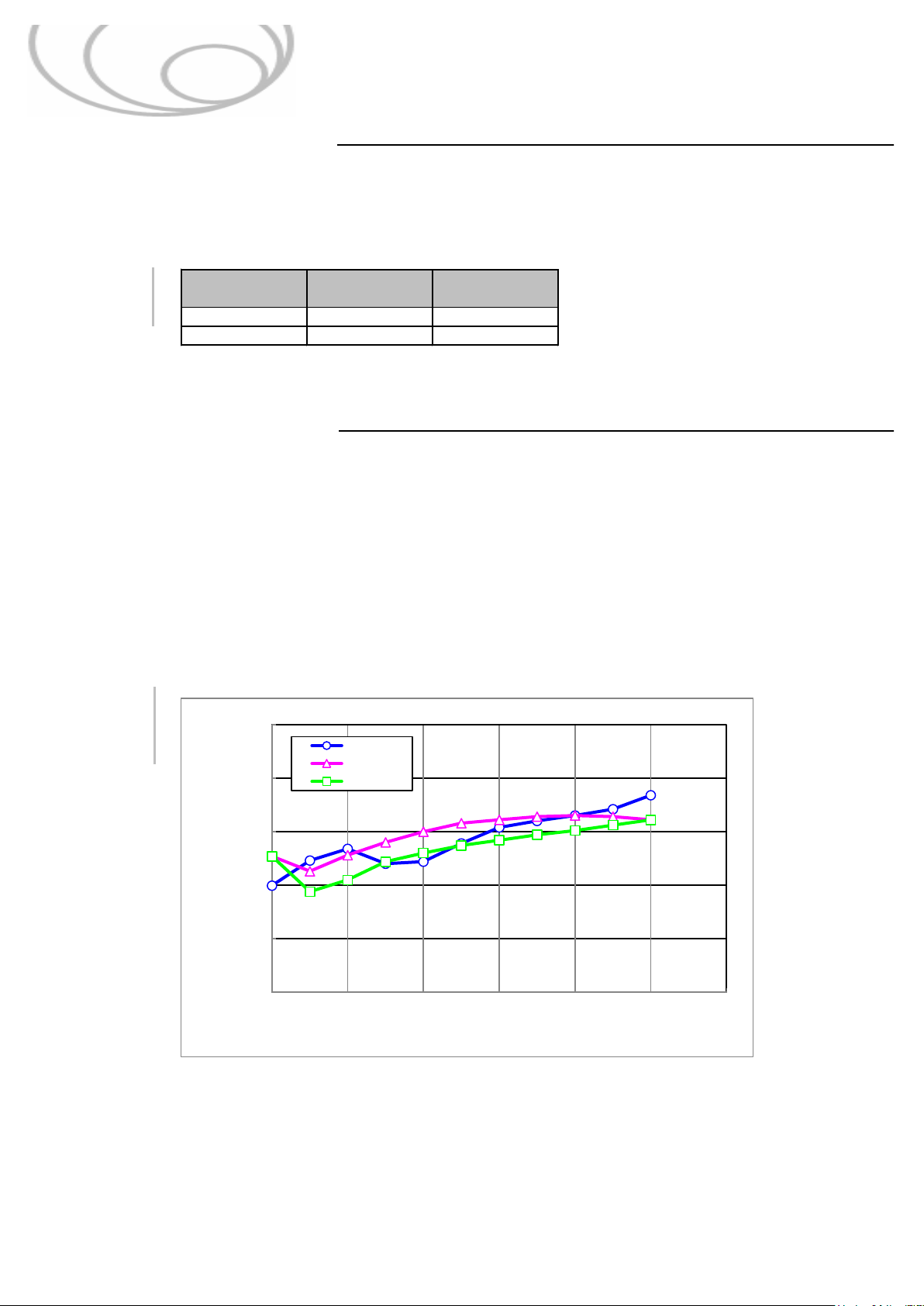
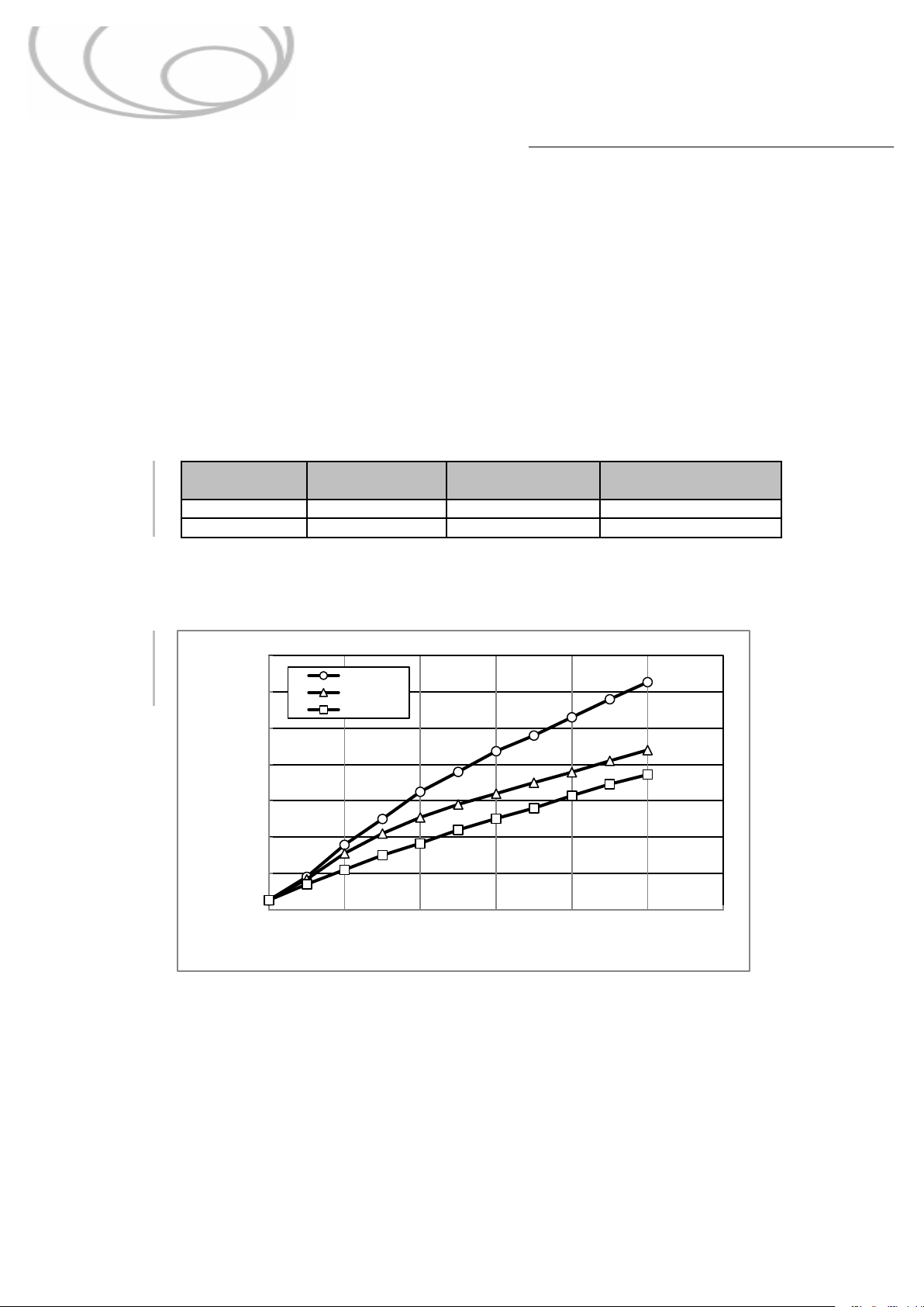
Table 2.1
Components list
・External parts should be changed according to the ambient temperature, and input and
For details, refer to the selection method of individual parts.
Applications Manual
TUNS1200
2. Connection for Standard Use
Heatsink
Rating Part name Rating Part name
1F11 AC250V/25A
0325025
(Littelfuse) AC500V/25A 0505025
(Littelfuse)
0325025
(Littelfuse) AC500V/25A 0505025
(Littelfuse)
For medical standard
application
LE155-MX × 2parallel
(OKAYA ELECTRIC INDUSTRIES)
LE155-MX × 2parallel
(OKAYA ELECTRIC INDUSTRIES)
AC400V
/2200pF
CD45-E2GA222M
(TDK)
AC400V
/2200pF
CD45-E2GA222M
(TDK)
SCR25-200-1R7A008JH
(TOKIN) 2.4mH/15A SCR25B-150-1R4A024J
(TOKIN)
SC15-E350H
(TOKIN) 2.4mH/15A SCR25B-150-1R4A024J
(TOKIN)
LE155-MX
(OKAYA ELECTRIC INDUSTRIES)
LE155-MX
(OKAYA ELECTRIC INDUSTRIES)
LE155-MX
(OKAYA ELECTRIC INDUSTRIES)
LE155-MX
(OKAYA ELECTRIC INDUSTRIES)
CD45-E2GA152M
(TDK) AC400V/1500pF CD45-E2GA152M
(TDK)
CD45-E2GA152M
(TDK) AC400V/1500pF CD45-E2GA152M
(TDK)
ELXZ250ELL222
(Nippon Chemi-Con) DC25V/2200uF ELXZ250ELL222
(Nippon Chemi-Con)
ELXZ500ELL102
(Nippon Chemi-Con) DC50V/1000uF ELXZ500ELL102
(Nippon Chemi-Con)
ELXZ630ELL471
(Nippon Chemi-Con) DC63V/470uF ELXZ630ELL471
(Nippon Chemi-Con)
C3216X7R1H105
(TDK) DC50V/1uF C3216X7R1H105
(TDK)
C3216X7R1H105
(TDK) DC50V/1uF C3216X7R1H105
(TDK)
C3216X7R2A105
(TDK) DC100V/1uF C3216X7R2A105
(TDK)
ELXS451VSN471 × 3parallel
(Nippon Chemi-Con)
ELXS501VSN471 × 3parallel
(Nippon Chemi-Con)
ECWFE2W105JA × 2parallel
(Panasonic Electronic Components)
ECWFE2J105JA × 2parallel
(Panasonic Electronic Components)
ECWFE2W105JA × 2parallel
(Panasonic Electronic Components)
ECWFE2J105JA × 2parallel
(Panasonic Electronic Components)
A5MC-5R1JK ×2series
(UCHIBASHI ESTEC)
A5MC-5R1JK ×2series
(UCHIBASHI ESTEC)
CRS32 683
(HOKURIKU ELECTRIC INDUSTRY)
CRS32 683
(HOKURIKU ELECTRIC INDUSTRY)
TND14V-621K
(Nippon Chemi-Con) 620V TND14V-621K
(Nippon Chemi-Con)
DSA-402MA
(Mitsubishi Materials) 4kV DSA-402MA
(Mitsubishi Materials)
Capacitor
for boost voltage
Capacitor
for boost voltage
Inrush current
protection resistor