Hirose BM56G Series Instruction Manual
TITLE:
BM56G Series Guideline
ETAD-H1035-00
HIROSE ELECTRIC CO.,LTD.
PRODUCT:
MULTI RF BOARD TO FPC CONNECTOR
Pitch:0.35mm, Width:2.2mm
Stacking height:0.6mm
PAGE: 1OF 13
BM56G Series Guideline
Approver
WR.FUKUCHI
20220121
Checker
TY.OOI
20220121
Designer
KT.KUSAKA
20220120
REVISIONS
RevNo
0
Designer
Checker
Approver
DATE
Jun.1.2022Copyright2022HIROSEELECTRICCO.,LTD.AllRightsReserved.

TITLE:
BM56G Series Guideline
ETAD-H1035-00
HIROSE ELECTRIC CO.,LTD.
PRODUCT:
MULTI RF BOARD TO FPC CONNECTOR
Pitch:0.35mm, Width:2.2mm
Stacking height:0.6mm
PAGE: 2OF 13
Table of contents
1. Notice for Device Handling........................................................................................................................................................ 3
1.1 Notice for mechanical designing............................................................................................................................................... 3
1.2 FPC fixing................................................................................................................................................................................. 3
1.3 Allocation of other components around connector ................................................................................................................... 4
1.4 Marking for mating position ..................................................................................................................................................... 4
2. Notice for PWB designing.......................................................................................................................................................... 5
2.1 Recommended PWB pattern and connector location................................................................................................................ 5
2.2 PWB designing ......................................................................................................................................................................... 7
2.3 FPC designing........................................................................................................................................................................... 7
3. Notice for Mounting ................................................................................................................................................................... 8
3.1 Metal mask design .................................................................................................................................................................... 8
3.2 Fillet forming ............................................................................................................................................................................ 8
3.3 Reflow Profile........................................................................................................................................................................... 8
4. Notice for Connector Handling................................................................................................................................................... 9
4.1 Connector insertion operation................................................................................................................................................... 9
4.2 Connector withdrawal operation............................................................................................................................................. 10
5. RF Evaluation Board Design Information ................................................................................................................................. 11
6. Additional information............................................................................................................................................................... 13
6.1 PWB cleaning ......................................................................................................................................................................... 13
6.2 PWB handling......................................................................................................................................................................... 13
6.3 Connector storage ................................................................................................................................................................... 13
Jun.1.2022Copyright2022HIROSEELECTRICCO.,LTD.AllRightsReserved.

TITLE:
BM56G Series Guideline
ETAD-H1035-00
HIROSE ELECTRIC CO.,LTD.
PRODUCT:
MULTI RF BOARD TO FPC CONNECTOR
Pitch:0.35mm, Width:2.2mm
Stacking height:0.6mm
PAGE: 3OF 13
Cover case
Buffer material
Stiffener
(Ex. FR-4)
FPC
PWB
(Ex. FR-4)
Cover case
1. Notice for Device Handling
1.1 Notice for mechanical designing
There is still possibility that connectors are disengaged if strong impact, such as dropping, is put against
connectors in use. In order to prevent connectors from disengaging, please make sure to put buffer material
between a connector and a cover case to hold down the connector pair to the mating direction.
If a connector is directly pressed down by a cover case, there is a possibility that the cover case is bent and it
may cause connector disengagement when the device is dropped. Please avoid a design that the connector is
directly pressed by cover case, instead, use put the buffer material to press down the connector.
Buffer material must be the size which is able to cover all over the connector mounting area.
1.2 FPC fixing
If FPC position is fixed, connector will get direct stress from dropping impact. Please do not design FPC
positioning bosses which prevent flexibility of FPC.
Without buffer material
Boss of cover
FPC
Jun.1.2022Copyright2022HIROSEELECTRICCO.,LTD.AllRightsReserved.

TITLE:
BM56G Series Guideline
ETAD-H1035-00
HIROSE ELECTRIC CO.,LTD.
PRODUCT:
MULTI RF BOARD TO FPC CONNECTOR
Pitch:0.35mm, Width:2.2mm
Stacking height:0.6mm
PAGE: 4OF 13
Please do not locate any material inside the red dashed.
Marking on PWB to
indicate appropriate
1.3 Allocation of other components around connector
Please do not locate any material which may effect on connector mating around the connectors.
1.4 Marking for mating position
When mating a connector on the FPC side against the other side manually, in order to operate mating in the
appropriate position without misalignment, please put some marking to indicate the exact mating position on
the PWB.
*For better mating operation, it is recommended that the
marking is done along the FPC outline.
2.2 MIN
3.7 MIN
Jun.1.2022Copyright2022HIROSEELECTRICCO.,LTD.AllRightsReserved.

TITLE:
BM56G Series Guideline
ETAD-H1035-00
HIROSE ELECTRIC CO.,LTD.
PRODUCT:
MULTI RF BOARD TO FPC CONNECTOR
Pitch:0.35mm, Width:2.2mm
Stacking height:0.6mm
PAGE: 5OF 13
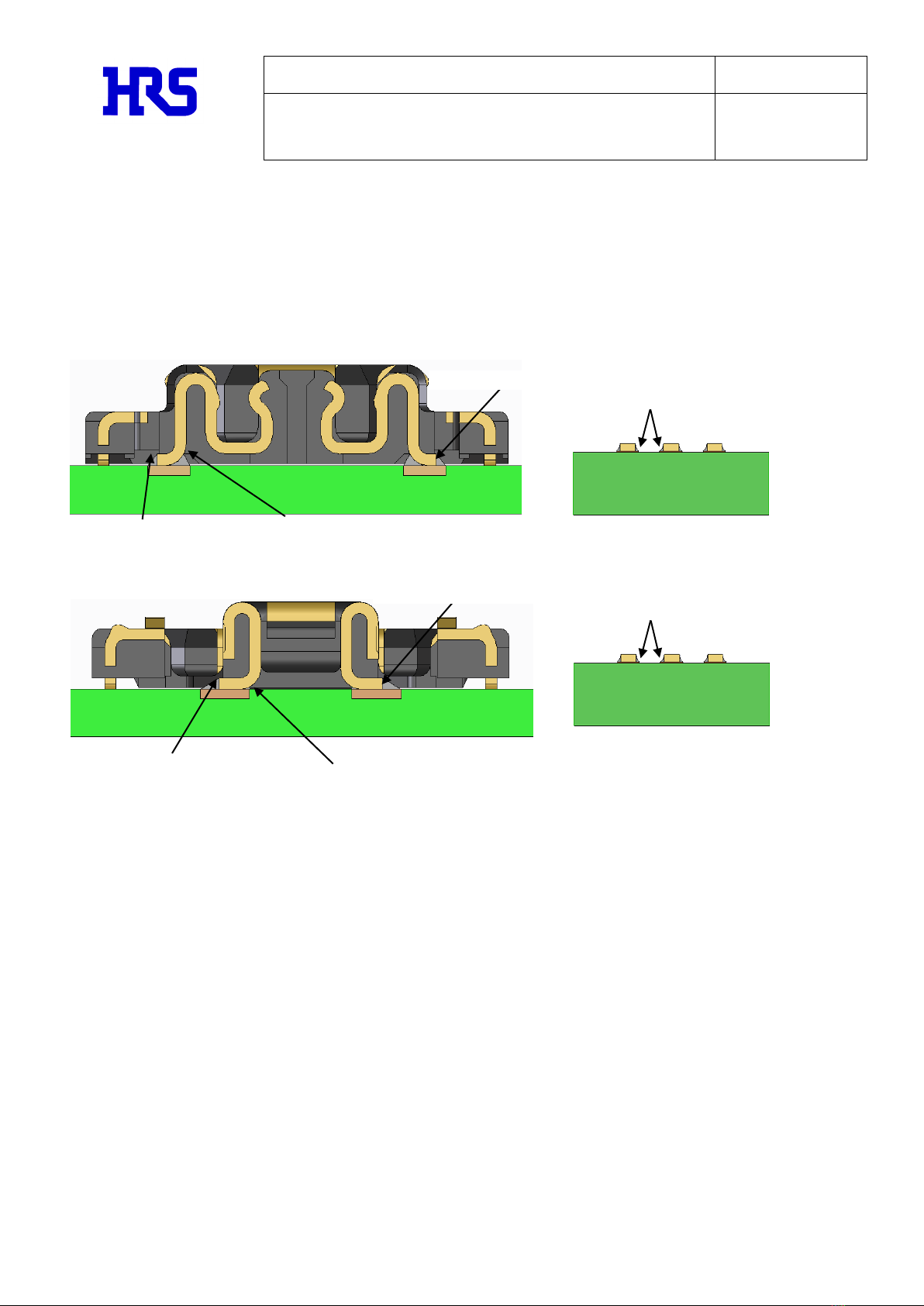
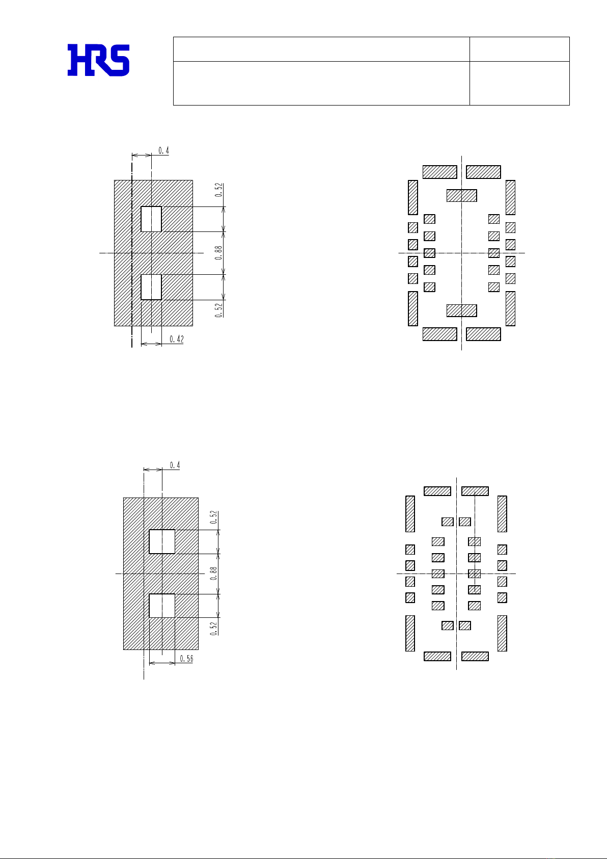
2. Notice for PWB designing
2.1 Recommended PWB pattern and connector location
For the recommended PWB pattern, please see the product drawing.
Pad layout and contact position for receptacle (A-A), A’
Pad layout and contact position for receptacle (B-B),B’
Pad layout and shield position for receptacle (C-C),C’
Pad layout and shield position for receptacle (D-D),D’
B
B
A
C
C
D
A’
B’
C’
D’
A
D
A
B
C
D
Jun.1.2022Copyright2022HIROSEELECTRICCO.,LTD.AllRightsReserved.
TITLE:
BM56G Series Guideline
ETAD-H1035-00
HIROSE ELECTRIC CO.,LTD.
PRODUCT:
MULTI RF BOARD TO FPC CONNECTOR
Pitch:0.35mm, Width:2.2mm
Stacking height:0.6mm
PAGE: 6OF 13
Pad layout and shield position for plug (E-E),E’
Pad layout and contact position for plug (F-F),F’
Pad layout and shield position for plug (G-G),G’
Pad layout and shield position for plug (H-H),H’
F
E
G
G
E’
F’
E
F
G’
H’
H
H
E
F
G
H
Jun.1.2022Copyright2022HIROSEELECTRICCO.,LTD.AllRightsReserved.

TITLE:
BM56G Series Guideline
ETAD-H1035-00
HIROSE ELECTRIC CO.,LTD.
PRODUCT:
MULTI RF BOARD TO FPC CONNECTOR
Pitch:0.35mm, Width:2.2mm
Stacking height:0.6mm
PAGE: 7OF 13
2.2 PWB designing
-Please design PWB layout properly so that front fillet, back fillet and side fillet are formed.
The recommended PWB layout is designed so that the connector can be soldered to the PWB appropriately.
- In case that the pad layout is narrower than our recommendation, If the pad layout is not wide enough, there is
a possibility that solder wicking or flux splashing may occur.
Please contact and discuss with us if the PWB layout is different from the recommended PWB layout.
-If there is not enough clearance on the inner side of PWB pattern, there is a possibility that the connector is
pushed up by solder paste.
-In case those patterns are designed under a connector, there is a possibility to cause solder failure if there are
physical height. Especially, in the following case, please conduct mounting test for the check.
2.3 FPC designing
Please make sure to put a stiffener on the backside of the FPC.
Pad peeling or connector bent may occur.
【Note】Please consult HRS contact window when you use thinner stiffer than our recommendation.
Please consider the warpage of the FPC board when mounting. Warpage may occur during heating.
(Max 0.02 mm at the center of the connector with reference to both ends of the connector).
Recommended thickness of stiffener
FR-4:0.3mm MIN
SUS:0.2mm MIN
Jun.1.2022Copyright2022HIROSEELECTRICCO.,LTD.AllRightsReserved.
TITLE:
BM56G Series Guideline
ETAD-H1035-00
HIROSE ELECTRIC CO.,LTD.
PRODUCT:
MULTI RF BOARD TO FPC CONNECTOR
Pitch:0.35mm, Width:2.2mm
Stacking height:0.6mm
PAGE: 8OF 13
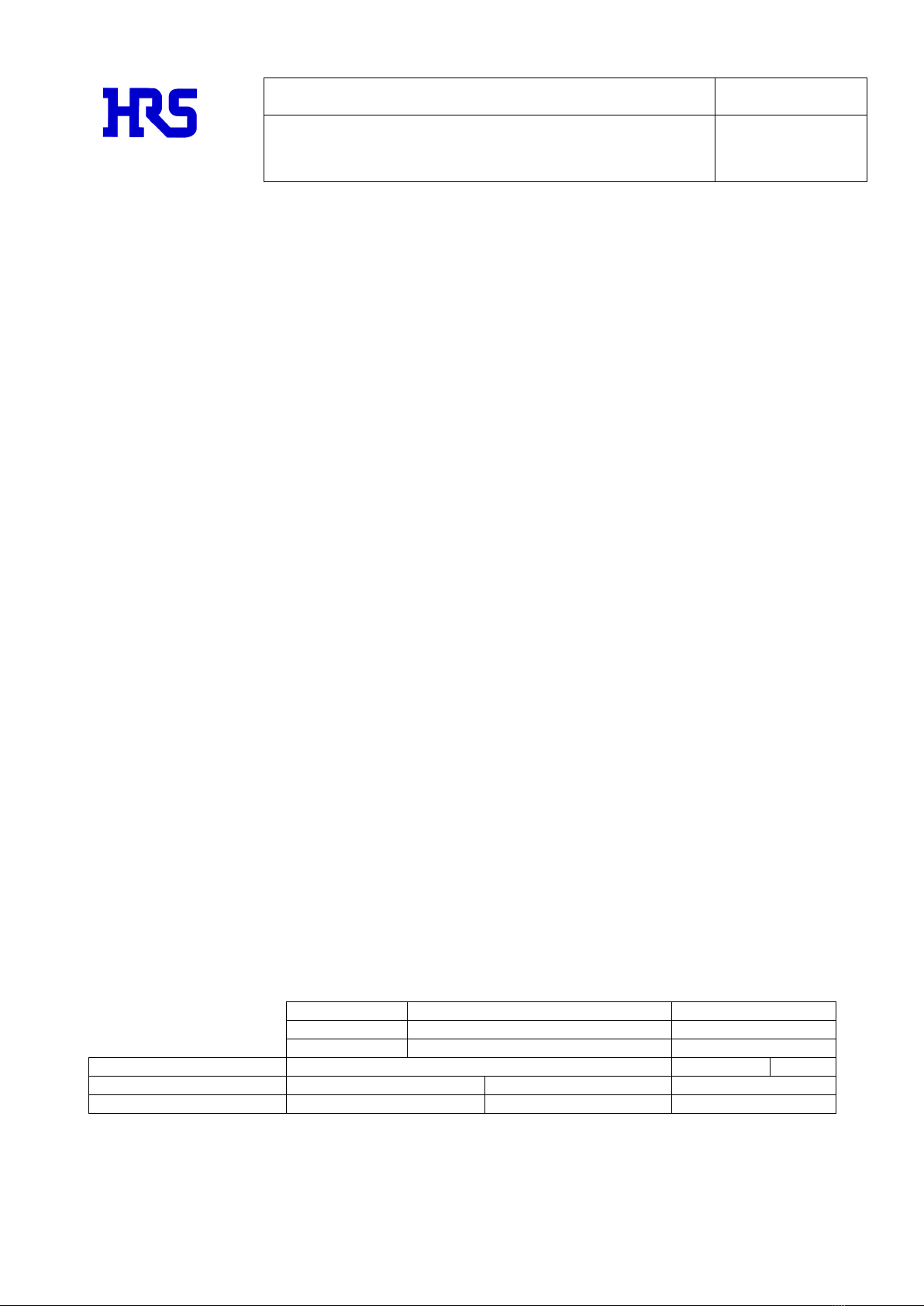
Side fillet
Side fillet
Front fillet
Back fillet
Front fillet
Back fillet
3. Notice for Mounting
3.1 Metal mask design
For the recommended metal mask design, please see the product drawing.
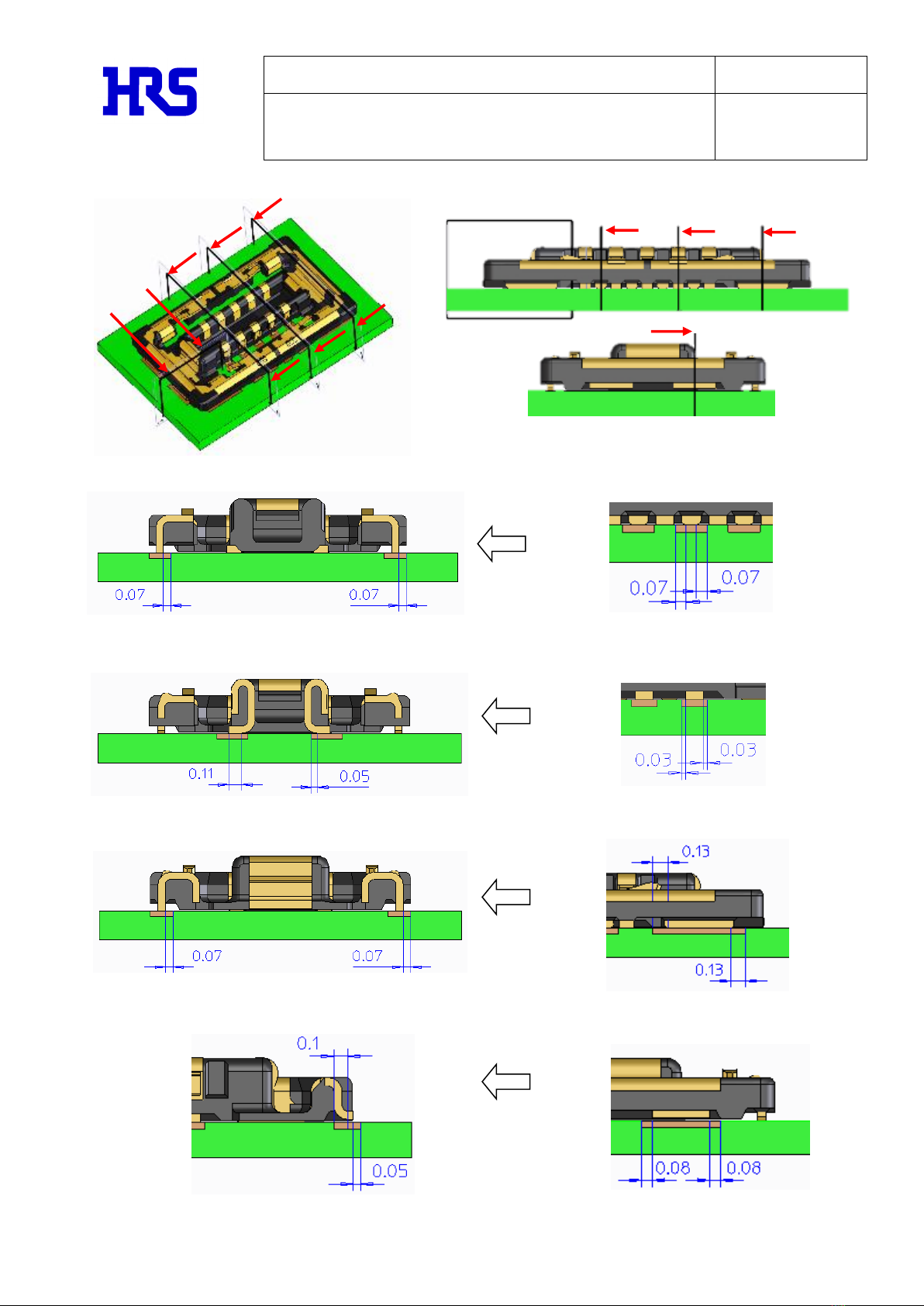
3.2 Fillet forming
Fillet forming on receptacle
Fillet forming on plug
Likewise the other (receptacle) side, as the contact lead edge, on where “front fillet” is formed is a metal cut surface,
phosphor bronze is exposed. The exposed area is easy to process thermal oxidation from reflow heating, so it is difficult for
soldering paste to get wet and be spread over the area. If the fillet formation needs to be judged defective/not defective,
please judge by “side fillet” forming.
3.3 Reflow Profile
For the recommended reflow profile, please see the product drawing.
Cut surface
Cut surface
Jun.1.2022Copyright2022HIROSEELECTRICCO.,LTD.AllRightsReserved.

TITLE:
BM56G Series Guideline
ETAD-H1035-00
HIROSE ELECTRIC CO.,LTD.
PRODUCT:
MULTI RF BOARD TO FPC CONNECTOR
Pitch:0.35mm, Width:2.2mm
Stacking height:0.6mm
PAGE: 9OF 13
4. Notice for Connector Handling
4.1 Connector insertion operation
Please mate this connector by hands.
Manual for inserting operation
1) Find the alignment area with hand to locate the connector in the appropriate mating position. This
connector has alignment chamber (guidance ribs) on receptacle side and R on plug side, so that the
connector can be self-aligned.
2) When the connector comes to the appropriate position, the connector comes into the aligned position.
If the connector comes into aligned position. It can be recognized by hand that the connector goes
down.
3) When the connectors are in alignment position, the connector pair cannot be moved back and forth and
around as they are mated in a parallel position. Please mate the connectors completely, by putting force
in this condition.
4) Please make sure connectors are mated completely. If one side is floating or the connectors are mated
at a slant, please unmate once, and then mate them once again, following the procedures above from
the beginning.
Go down one level
Jun.1.2022Copyright2022HIROSEELECTRICCO.,LTD.AllRightsReserved.

TITLE:
BM56G Series Guideline
ETAD-H1035-00
HIROSE ELECTRIC CO.,LTD.
PRODUCT:
MULTI RF BOARD TO FPC CONNECTOR
Pitch:0.35mm, Width:2.2mm
Stacking height:0.6mm
PAGE: 10 OF 13
4.2 Connector withdrawal operation
1) It is desirable to withdraw the connector in the vertical direction against mating direction. However, in the
case connector has high pin counts or thinner FPC and stiffener, it makes more difficult to withdraw the
connector in the vertical direction.
2) If it is difficult to withdraw the connector, please withdraw the connector diagonally against the contact
pitch direction. Please carefully withdraw the connector from the width side as a strong load is put on the
plug.
3) If the FPC is not strong enough, there is a possibility that contacts may be pulled off or broken. Please make
sure to conduct the test on FPC to repeat operation several times in an early stage build. Please carefully
withdraw the connector in the slanted direction, picking the FPC corner, as it can be a risk to put a strong
load on contacts.
Jun.1.2022Copyright2022HIROSEELECTRICCO.,LTD.AllRightsReserved.

TITLE:
BM56G Series Guideline
ETAD-H1035-00
HIROSE ELECTRIC CO.,LTD.
PRODUCT:
MULTI RF BOARD TO FPC CONNECTOR
Pitch:0.35mm, Width:2.2mm
Stacking height:0.6mm
PAGE: 11 OF 13
5. RF Evaluation Board Design Information
The followings are the examples of board layers, patterns, and cutout dimensions. For the recommended
PWD pattern, please see the product drawing.
Please use the thickness’ information of the each layers as a reference, and please modify/control the
impedance of this product at 50Ω±10%.
Recommendation for the coaxial connector part is a Hirose’s product: HK-LR-SR2 (K connector: 2.92mm).
Please optimize the BM56 and the coaxial (HK-LR SR2) part by cutting out the L2 layer.
Example: Board Layers Example: Pattern Width (mm)
Jun.1.2022Copyright2022HIROSEELECTRICCO.,LTD.AllRightsReserved.
TITLE:
BM56G Series Guideline
ETAD-H1035-00
HIROSE ELECTRIC CO.,LTD.
PRODUCT:
MULTI RF BOARD TO FPC CONNECTOR
Pitch:0.35mm, Width:2.2mm
Stacking height:0.6mm
PAGE: 12 OF 13
Receptacle RF Evaluation Board: Example of the cutout dimension
Plug RF Evaluation Board: Example of the cutout dimension
S
S
G
G
G
G
G
G
G
G
S
S
G
G
G
G
G
G
G
G
Pin Assignment: Ex.
S:RF Signal
G:GND
Pin Assignment: Ex.
S:RF Signal
G:GND
Example of Cutout Dimension(mm)
Example of Cutout Dimension(mm)
Jun.1.2022Copyright2022HIROSEELECTRICCO.,LTD.AllRightsReserved.

TITLE:
BM56G Series Guideline
ETAD-H1035-00
HIROSE ELECTRIC CO.,LTD.
PRODUCT:
MULTI RF BOARD TO FPC CONNECTOR
Pitch:0.35mm, Width:2.2mm
Stacking height:0.6mm
PAGE: 13 OF 13
6. Additional information
6.1 PWB cleaning
Do not wash the board because it may be cause malfunction of the connector.
6.2 PWB handling
In the operation which could give stress to the mounted connector, including cutting or bending PWB, keep
soldering area from mechanical stress.
6.3 Connector storage
1) Void could be occurred on the housing surface due to high heat during reflow. In order to prevent this
problem, avoid storing connectors under humid condition. For long term storage, keep them at humidity
manageable place.
2) Depending on the production LOT of the connector, its housing color could be varied, or ultraviolet during
storage changes connector surface color. However, these color differences do not affect the connector
performance.
3) During PWB assembly and module assembly, make sure not to apply excessive stress to the stored
connectors.
4) Avoid storing connectors in dusty area, or it could cause contact failure.
End of report
Jun.1.2022Copyright2022HIROSEELECTRICCO.,LTD.AllRightsReserved.
Table of contents
Other Hirose Cables And Connectors manuals

Hirose
Hirose EnerBee DF60 Series User manual

Hirose
Hirose FH63 Series Manual

Hirose
Hirose DF53 Series Manual

Hirose
Hirose DF62W Series Manual

Hirose
Hirose GT43 User manual

Hirose
Hirose BM10 Series User manual

Hirose
Hirose GT16G-1S-HU User manual

Hirose
Hirose GT50 Series User manual
 User manual")
Hirose
Hirose DF62WZ-6P-2.2DSA(20) User manual

Hirose
Hirose EnerBee DF60 Series User manual


