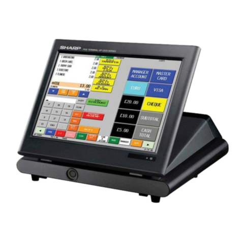
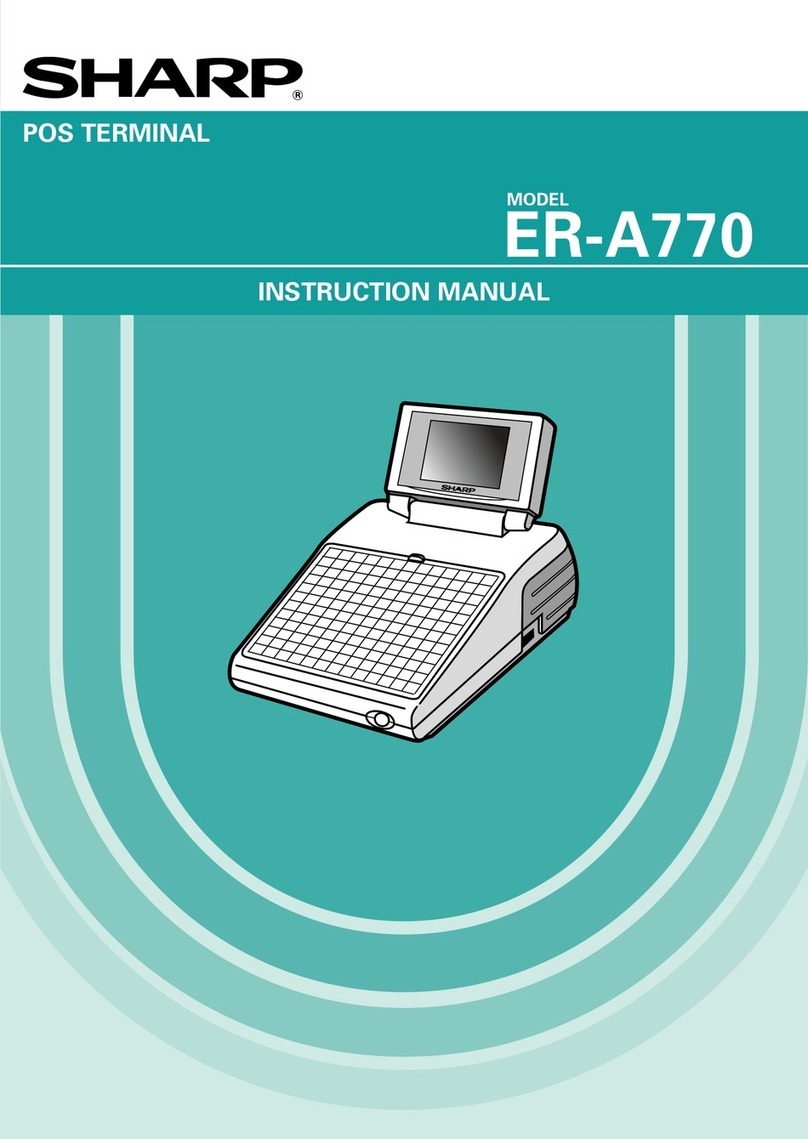
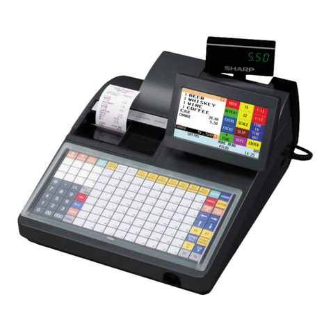
Sharp UP-5300 User manual

CODE: 00ZUP5300USME
POS TERMINAL
MODEL UP-5300
("U" & "A" version)
CHAPTER 1. SPECIFICATIONS . . . . . . . . . . . . . . . . . . . . . . . . . . . 1-1
CHAPTER 2. OPTIONS . . . . . . . . . . . . . . . . . . . . . . . . . . . . . . . . . . 2-1
CHAPTER 3. SERVICE PRECAUTION . . . . . . . . . . . . . . . . . . . . . 3-1
CHAPTER 4. UP-5300 DIAGNOSTICS SPECIFICATIONS . . . . . . 4-1
CHAPTER 5. CIRCUIT DESCRIPTION . . . . . . . . . . . . . . . . . . . . . 5-1
CHAPTER 6. BIOS SETUP UTILITY . . . . . . . . . . . . . . . . . . . . . . . . 6-1
CHAPTER 7. ABOUT UTILITY SOFTWARE AND OTHERS . . . . . 7-1
CHAPTER 8. CIRCUIT DIAGRAM . . . . . . . . . . . . . . . . . . . . . . . . . 8-1
CHAPTER 9. PWB LAYOUT . . . . . . . . . . . . . . . . . . . . . . . . . . . . . . 9-1
PARTS GUIDE
CONTENTS
SHARP CORPORATION
Parts marked with "!" is important for maintaining the safety of the set. Be sure to replace these parts with specified
ones for maintaining the safety and performance of the set.
This document has been published to be used
for after sales service only.
The contents are subject to change without notice.

BATTERY DISPOSAL
Contains Nickel Metal Hydride Battery. Must be Disposed of Properly.
Contact Local Environmental Officials for Disposal Instructions.

CHAPTER 1. SPECIFICATIONS
1. Appearance
AC cord
Plug your POS terminal into a wall outlet before using.
Power switch
Set the power switch to the ON ( I ) position after plugging your POS
terminal.
2. Rating
ITEM SPECIFICATIONS
External dimensions 11.6 (W) ×16.3 (D) ×12.6 (H) in.
approximately (295 (W) ×414.5 (D) ×
320 (H) mm)
Weight Approximately 13.9 lb. (5.9 kg)
Power source 120V AC ±10%, 60 Hz
Power consumption Operating : 63W
Working temperature
and humidity 32 to 104°F (0 to 40°C)
10 to 90%
3. Hardware
3-1. Display
ITEM SPECIFICATIONS NOTE
Type DSTN color LCD with back
light With 256 colors
Screen size 10.4" Full screen
Dot format 640 (W) ×480 (H) dots
Dot size 0.33 ×0.33 mm
Control VGA
3-2. Keyboard
ITEM SPECIFICATIONS NOTE
Type Touch key
(Analog touch panel)
Number of key
positions 4096 (W) ×4096 (H)
positions
Control Mouse emulation
3-3. PC system
ITEM SPECIFICATIONS NOTE
CPU Pentium processor
Chip set FireStar Plus:
82C700U3.2
Graphic controller VGAC : MN89305
Main memory
(for executing MS-DOS,
Application software)
Standard : 8
Mbytes EDO type
Max. : 40 Mbytes adding S.O.DIMM
Video RAM 1 Mbytes EDO type
BIOS ROM 512 Kbytes Flash ROM
OS (MS-DOS) ROM 4 Mbytes Mask ROM
ROM disk memory
(for stored Application
software)
Standard : 2
Mbytes Flash ROM
Max. : 6 Mbytes adding UP-F04RB
RAM disk memory
(for POS data) Standard : 1
Mbytes PS-RAM
Max. : 3 Mbytes adding UP-P02MB
Keyboard controller M38802M270
Super I/O M5113 A2
POS system controller PSC2 : LZ9AM22
3-4. Serial port
D-SUB 9-pin connector COM1 and COM2 are equipped.
In order to supply +5V power, CI signal and +5V power supply of
COM1 and COM2 can be switched.
2 channels of RJ45 Connector COM port are equipped.
COM3 and COM4 or original I/O address (COM5 and COM6) can be
selected as the 2 channels of RJ45 COM port.
COM1 & COM2: D-sub 9 pin
Pin No. Signal Function I/O
1 CD Data Carrier Detect I
2 RD Receive Data I
3 SD Send Data O
4 ER Data Terminal Ready O
5 SG Signal Ground —
6 DR Data set Ready I
7 RS Request to Send O
8 CS Clear to Send I
9 CI/+5V Ring Indicate / +5V I/–
COM3 or COM5: Modular jack RJ45 8 pin
Pin No. Signal Function I/O
1 RS Request to Send O
2 ER Data terminal Ready I
3 SD Send Data O
4 SG/(+5V) Signal Ground/(+5V) —
5 SG Signal Ground –
6 RD Receive Data I
7 DR Data set Ready I
8 CS Clear to Send I
1 – 1
COM4 or COM6: Modular jack RJ45 8 pin
Pin No. Signal Function I/O
1 RS Request to Send O
2 ER Data terminal Ready I
3 SD Send Data O
4 SG Signal Ground —
5 SG Signal Ground –
6 RD Receive Data I
7 DR Data set Ready I
8 CS Clear to Send I
3-5. Expansion slot
ITEM SPECIFICATIONS NOTE
Type ISA bus Half size PC board
Number of slots 2 slots
Power consumption +5V/max. 1.0A
+12V/max. 0.05A
3-6. Shutdown switch
The shutdown switch is used when the OS or application programs
are straying and the system can not return to the normal state.
You must not use this shutdown switch when the UP-5300 is running
normally. Use this switch only when the main power source is not cut
off even if the main unit power switch is set to OFF position. UP-5300
is turned OFF and the hardware is reset by turning the main power
switch OFF and then pressing the shutdown switch.
[Out line]
The shutdown switch is single shot type. (Normally OFF position)
Push ON: This position is used to reset stand-by mode for power
supply unit when software hang up.
Release OFF: Usually the shutdown switch needs to be set to this
position when the UP-5300 is operated.
[Operating method]
The shutdown switch is a push switch. If it is pushed to ON, the
UP-5300 stops supplying the power when the power switch is set into
stand-by mode.
NOTE: The shutdown operation will be ignored when te power
switch is set into power-on position.
3-7. System switch
The system switches are used to preset various system configura-
tions.
[Out line]
The system switches consists of DIP switches.
[DIP switch]
The PSC2 simply reads the switched signals from the DIP switch as
hardware. The meaning of the switche settings are shown on the next
page.
12345678
Shutdow n sw itch
12345678
S
y
stem sw itch
1 – 2

: Default setting
DSW-8
Function OFF
(value=1) ON(value=0)
Serial 3 & 4
decode mode COM3 &
COM4 COM5 &
COM6
DSW-7
Function OFF
(value=1) ON(value=0)
COM3 &
COM4 IRQ
assign
(Serial 3 & 4)
COM3 =
IRQ11
COM4 =
IRQ10
COM3 =
IRQ4
COM4 =
IRQ3
DSW-6
Function OFF
(value=1) ON(value=0)
CMOS
Initialize Not Initialize Initialize
DSW-5
DSW-4
Drive C:, D: & E: Setting
Drive
C: Drive
D: Drive
E: DSW-4 DSW-5
HDD — — ON
(value=0) ON
(value=0)
HDD PS
RAM Flash
ROM ON
(value=0) OFF
(value=1)
PS
RAM Flash
ROM HDD OFF
(value=1) ON
(value=0)
Flash
ROM PS
RAM HDD OFF
(value=1) OFF
(value=1)
DSW-3
Function OFF
(value=1) ON(value=0)
Boot Drive Drive A: Drive C:
DSW-2
Function OFF
(value=1) ON(value=0)
Drive A:
Device Mask ROM FDD
DSW-1
Function OFF
(value=1) ON(value=0)
Floppy Disk
Controller Not Exit Exit
3-8. Power switch
[Out line]
The power switch has the positions ON and OFF (Stand-by)
ON position: Usually the power switch needs to be set to this posi-
tion when the POS-terminal is operated.
OFF position: This position is used to turn the stand-by mode. When
the power switch is set to this position, the power
supply stops automatically. But if the software pro-
gram controls the power supply to hold, even if the
power switch is set into this position, power is supplied
until an software program allows power supply no to
hold.
[Operating method]
The power switch is a see-saw switch, and it can be tipped toward
the ON or OFF.
4. Software
4-1. Software Structure
The basic system software mainly consists of the following 3
modules.
(1) MS-DOS Version 6.22
The operating system (MS-DOS Version 6.22) is stored in a MROM
disk.
(2) Drivers
There are following types of drivers
•POS Device Drivers (for Clerk, Buzzer, Drawer, Timer, MCR, Line
Display, Serial Port) POS device drivers adopt the same control
method as previous (ER-A850/A880/UP-5700) softwares.
•Touch Panel Driver
(3) POS Device Middleware
The middleware has been developed to improve the performance of
applications.
(4) Software Structure
ON
OFF
ON
1234567 8
Power switch :
Application
POS Utillty
POS Device
Mifddle Wsre
MS-DOS Version 6.22
Touch
Panel
Driver POS Devlce Driver
BIOS
Provided from SHARP Corporation
Hardware
Standard PC
Device Driver
(Local production)
SCSI
Ethernet
.......etc
1 – 3

4-2. Basic system software list
ITEM CONTENTS for UP-5300 for PC
BIOS (FROM) •AT compatible system BIOS
F—
•VGA BIOS for MN89305 VGA LSI
•Standard SETUP program
•Flash Disk/MROM Disk/PSRAM Disk built-in control program
•Memory size/HDD type auto detect function
•No APM/PnP support
OS (MROM disk) MS-DOS Version 6.22 (Subset)
Install program (MROM disk) •System Install program
•APL Install program (for MS-DOS/Windows 95/98/NT) — F
POS device driver •POS device driver F—
•Touch panel driver (mouse emulation I/F only) F—
Middleware software and
application development tools •POS device MiddleWare F—
•Printer Logo image loading utility program (MS-DOS/Windows 95) FF
•Touch panel calibration utility program (MS-DOS) F—
... These software are provided with FD from SHARP corporation.
Please copy contents of FD provided from department to development PC. Install to UP-5300 by using APL Install Program from PC.
4-3. Memory map
0000000h
0800000h
1000000h
1800000h
2800000h
STD. 8MB
+8MB
(16MB)
+8MB
(24MB)
+32MB
(40MB)
00000h
9F4000h
A0000h
C0000h
C8000h
E8000h
100000h
MS-DOS
(25K)
Sharp Driver
(32K)
Free
Conventional
(580K)
EBDA : 3K
VRAM
128K
VGA BIOS(32K)
UMB
(124K)
System BIOS
(96k)
HMA
64K
POS Device 20K
Touch Key 12k
(External BIOS
Data Area)
Middleware Not used
00000h
9F4000h
A0000h
C0000h
C8000h
E8000h
100000h
MS-DOS
(25K)
Sharp Driver
(32K)
Free
Conventional
(565K)
EBDA:3K
VRAM
128K
VGA BIOS(32K)
UMB
(124K)
System BIOS
(96k)
HMA
64K
POS Device 20K
Touch Key 12k
(External BIOS
Data Area)
Middleware is used
Middleware
(15K)
Memory is expandable up to
40MB max. using EMM386 in DOS
1 – 4

CHAPTER 2. OPTIONS
1. System configuration
AT Keyboard
<supplied on site>
Incorporated in Main Unit RS-232 Communication Connection
max.2 (RS-232)
Drawer
<Option>
ER-03DW/
04W/05DW
(In Europe only)
Customer
Poll Display
<Option>
UP-P20DP
Additional
RAM Memory
<Option>
UP-P02MB
Additional
ROM Memory
<Option>
UP-F04RB
Additional DRAM
Memory
<supplied on site>
Magnetic
Card Reader
<Option>
UP-E12MR
HDD Unit
<supplied on site>
RS232 Board
<Option>
ER-A8RS
Ethernet Board
<supplied on site>
In-line Communication
Connection
UP-5300
Centronics Printer
<supplied on site>
Remote Printer
<Option> ER-01PU
<supplied on site>
Kitchen video monitor
<supplied on site>
(For North America only)
CAT/FET
<supplied on site>
TM-T80/85/295
ER-FBT40
Hand Scanner
<Option>
ER-A6HS1
UP-5300
PC
<supplied on site>
Built-in,
customer-side
display
<Option>
UP-I20DP
(NEW)
Built-in printer
<Option>
UP-T80BP
(Standard4channels)
(Additional 2 channels)
Host PC
Scale
<supplied on site>
Coin dispenser
<supplied on site>
(For North America only)
Drink dispenser
<supplied on site>
(For Europe only)
2. Options
No. NAME MODEL NAME DESCRRIPTION
1 Expansion RAM disk board UP-P02MB 2 Mbytes RAM board
2 Expansion ROM disk board UP-F04RB 4 Mbytes ROM board
3 Customer display UP-I20DP 2 line 20 digits dot display
4 Customer pole display UP-P20DP 2 line 20 digits dot display
5 MCR (Magnetic Card Reader) UP-E12MR2 for ISO 1 & 2 stripe card
6 Remote drawer ER-03DW 7B/5C
ER-04DW 5B/5C
7 Receipt/Journal printer ER-01PU 2 station (R/J) thermal printer 45mm width
8 Built-in printer UP-T80BP 1 station thermal printer 80mm width
9 RS232 & CENTRO I/F board ER-A8RS RS232 9 pins connector:2 ports
Centronics 25 pins connector : 1 port
10 Hand scanner ER-A6HS1 for reading bar code
11 FDD unit HZ-H14FD 3.5" Floppy Disk Drive (Newtronics D353M3)
2 – 1
3. Locally supplied options
No. NAME MODEL NAME DESCRIPTION
1 S.O.DIMM Small Outline DIMM Max. 32Mbyte *1
2 HDD (by FUJITSU) MHD2021AT 2.5 inch, 2.1Gbyte *2
3 PC keyboard PS/2 type PC keyboard
4 Application software
5 Additional device drivers
*1 EXTENSION RAM MODULE (Provided through SHARP Electronics Corporation)
[Outline] UP-5300 has a socket as Small Outline DIMM.
It is necessary to satisfy with S.O.DIMM memory specification as follows.
[Specification]
144pin S.O.DIMM
8 Mbytes 16 Mbytes 32 Mbytes
TYPE EDO type
ACCESS TIME 60 nsec. (less than)
POWER 3.3 V
REFRESH CYCLE 1024/16 msec. 2048/32 msec. 4096/64 msec.
REFRESH TYPE CBR
POWER CONSUMPTION 700 mA (less than)
OTHER 4 chip ×16 Mbits
(1 Mwords ×16 bits) 8 chip ×16 Mbits
(2 Mwords ×8 bits) 4 chip ×64 Mbits
(4 Mwords ×16 bits)
*2 HARD DISK DRIVE (Local purchase)
[Outline] UP-5300 may be connected to the Hard Disk Drive.
It is necessary to satisfy the 2.5 inch Hard Disk Drive specification as follows.
[Specification]
2.5 inch type Hard Disk Drive
MAKER FUJITSU
MODEL MHD2021AT
PARTS No.
REVISION No. 1) Part No.: CA01640-B040
Rev. No.: A4
CAPACITY 2.16 Gbytes
INTERFACE ATA-3
4. Service options
No. NAME PARTS CODE PRICE DESCRIPTION
1 Connector cable for Dongle (LPT-1) QCNW-7858BHZZ BL Relay line from Terminal to Dongle
2 HDD mounting kit DKIT-8671RCZZ — Bracked assembly for mounting
5. Service tools
No. NAME PARTS CODE PRICE DESCRIPTION
1 Service tool kit DKIT-8656BHZZ CW ISA checker
ISA relay board
2 Printer connector signal loop back connector UKOG-6717RCZZ BR for ER-A8RS CENTRONICS connector
3 MCR test card UKOG-6718RCZZ BE for UP-E12MR
4 RS232 loop back connector UKOG-6705RCZZ BC for RS232 connector
5 CPU/VGA PWB relay PWB CKOG-6728BHZZ CQ
6 BIOS loading board CKOG-6727BHZZ CS for overwriting BIOS
7 RS232 modular jack loop back connector UKOG-6729BHZZ AZ for RJ45 connector
8 BIOS MASTER ROM VHI27040RBQ1A (P) EP-ROM for overwriting BIOS
9 TOUCH PEN CPENP1004PCN5 AG
2 – 2

4-1. Service tool kit: DKIT-8656BHZZ
1) ISA checker
Used to repair or check the operation of the optional I/F.
•External view
•Plain view
•Connection diagram
2) ISA relay board
Connected to the ISA checker for installation of the optional I/F
horizontally and for repairing and checking the operation .
•External view
•Plain view
RAM1A
LED circuit: Not used currently.
Test pins: Used to check the ISA bus signal.
ISA bus connectors:
Used to connect with the I/F PWB of ER-A8RS etc.
Connected to the UP-5300 ISA bus connectors.
UP-5300
ISA bus connector
ER-A8RS
ISA checker
ISA bus connector:
Used to check the ER-A8RS solder side.
Connected to the ISA bus connector of ISA checker.
ISA bus connector:
Used to check the ER-A8RS parts side.
2 – 3

•Connection diagram
4-2. Printer connector signal loop check cable:
UKOG-6717RCZZ
Connected to the centronics connector (25 pin) of the ER-A8RS, and
is used to check loop signals when executing diagnostics.
•External view
•Plan view and connection diagram
•Connection diagram
4-3. MCR test card: UKOG-6718RCZZ
•Used when executing the diagnostics of the UP-E12MR2.
•External view
ER-A8RS solder side
ISA relay board
ER-A8RS parts side
ISA PWB
ISA checker
150±8
Signal name Pin No.
1STROBE- 2DB0 3DB1 4DB2 5DB3 6DB4 7DB5 8DB6 9DB7 10ACK- 11BUSY 12PE 13SLCT 14AUTOFD- 15ERROR- 16INIT- 17SLCTIN- 18~25PE
Signal namePin No.
1 STROBE-
2 DB0
3 DB1
4 DB2
5 DB3
6 DB4
7 DB5
8 DB6
9 DB7
10 ACK-
11 BUSY
12 PE
13 SLCT
14 AUTOFD-
15 ERROR-
16 INIT-
17 SLCTIN-
18~25 PE
ER-A8RS
2 – 4

4-4. RS232 loop back connector: UKOG-6705RCZZ
Connected to the RS232 connector (D-SUB 9 pin: COM1, COM2,
COM3, COM4) of the UP-5300 and ER-A8RS, and used to check
loop signals when executing diagnostics.
•Connection diagram
4-5. RS232 modular jack loop back connector:
UKOG-6729BHZZ
Connected to the RS232 connector (RJ45: COM3, COM4, COM5,
COM6) of the UP-5300, and used to check loop signals when execut-
ing diagnostics.
•Connection diagram
4-6. BIOS loading board: CKOG-6727BHZZ
The BIOS loading board: CKOG-6727BHZZ is a tool to write a BIOS
ROM program in the F-ROM on the UP-5300’s main board. Use this
PWB in the following cases:
•The F-ROM on the UP-5300’s main board be comes unreadible
and a BIOS ROM program must be written in the F-ROM.
•The BIOS ROM program in the F-ROM is overwritten due to the
version up of BIOS ROM program, etc.
The BIOS loading board is connected to the Option ROM/RAM disk
connector (CN5) of the Main PWB.
•External view
•Plain view
•Connection diagram
CD 1pin
RD 2pin
TD 3pin
DTR 4pin
GND 5pin
DSR 6pin
RTS 7pin
CTS 8pin
RI 9pin
RTS
DTR
TD
GND
GND
RD
DSR
CTS
1pin
2pin
3pin
4pin
5pin
6pin
7pin
8pin
LED1 LED2 LED3 LED4 LED5 LED6 LED7 LED8
13
SW1
2 – 5

Writing BIOS ROM Program
NOTE: Remove all option boards from the ISA slots before writing
on the BIOS ROM.
1. Install the EP-ROM (master ROM): containing a BIOS program on
the BIOS loading board: CKOG-6727RCZZ.
*Caution: The AC power must be removed prior to installing the
BIOS loading board.
2. Set SW1 on the BIOS loading board to the side of pin 3.
BIOS MASTER ROM
LED1 LED2 LED3 LED4 LED5 LED6 LED7 LED8
LED9
SW1
13
SW1
13
SW1
2 – 6

3. Open the upper cabinet.
4. Connect the BIOS loading board to the option ROM/RAM connec-
tor CN5 on the main PWB, and then close the cabinet.
5. Writing the BIOS ROM program starts by turning on the power
switch on the right side.
To determine the status of the LED lights on the special service
PWB when a BIOS ROM program is being written, see the table
on the next page.
Writing is complete (automatic completion) when the green LED
(LED9) on the BIOS loading board lights up.
6. After writing is complete, turn off the power switch on the right side
to remove the BIOS loading board, and turn on the power switch
on the left side again to check whether the BIOS program starts
up normally or not.
LED DISPLAY STATUS
[E: ON (Lighting) — : OFF]
<In normal operation>
LED1
(RED) LED2
(RED) LED3
(RED) LED4
(RED) LED5
(RED) LED6
(RED) LED7
(RED) LED8
(RED) LED9
(GREEN) FUNCTION
EEEEEEEE— Start of COPY FUNCTION
————E————Start initializing
—————E— — — Erasing F-ROM (LED6: RED is blinking)
————EE———
Start copy programming to F-ROM from EP-
ROM
————EE— — — Programming: Bank0 C0000 h (64KB)
E———EE— — — Programming: Bank0 D0000 h (64KB)
—E——EE— — — Programming: Bank0 E0000 h (64KB)
EE——EE— — — Programming: Bank0 F0000 h (64KB)
———EEE— — — Programming: Bank1 C0000 h (64KB)
E——EEE— — — Programming: Bank1 D0000 h (64KB)
—E—EEE— — — Programming: Bank1 E0000 h (64KB)
EE—EEE— — — Programming: Bank1 F0000 h (64KB)
——————E— — Start verifying the program in the F-ROM
——————E— — Verifying: Bank0 C0000 h (64KB)
E—————E— — Verifying: Bank0 D0000 h (64KB)
—E————E— — Verifying: Bank0 E0000 h (64KB)
EE————E— — Verifying: Bank0 F0000 h (64KB)
———E——E— — Verifying: Bank1 C0000 h (64KB)
E——E——E— — Verifying: Bank1 D0000 h (64KB)
—E—E——E— — Verifying: Bank1 E0000 h (64KB)
EE—E——E— — Verifying: Bank1 F0000 h (64KB)
————E—E— — Setting protection the F-ROM
EEEEEEEEEEND of complete COPY FUNCTION
2 – 7

<Erase ERROR in F-ROM>
LED1
(RED) LED2
(RED) LED3
(RED) LED4
(RED) LED5
(RED) LED6
(RED) LED7
(RED) LED8
(RED) LED9
(GREEN) FUNCTION
E————E—E— Device not ready
—E———E—E— VPP error
EE———E—E— Command sequence error
——E——E—E—
<Programming ERROR in F-ROM>
LED1
(RED) LED2
(RED) LED3
(RED) LED4
(RED) LED5
(RED) LED6
(RED) LED7
(RED) LED8
(RED) LED9
(GREEN) FUNCTION
E———EE—E— Device not ready
—E——EE—E— VPP error
EE——EE—E— Command sequence error
<Verifying ERROR in F-ROM>
LED1
(RED) LED2
(RED) LED3
(RED) LED4
(RED) LED5
(RED) LED6
(RED) LED7
(RED) LED8
(RED) LED9
(GREEN) FUNCTION
E———E—EE— Device not ready while release the protection
—E——E—EE— Can not release the protection
2 – 8

CHAPTER 3. SERVICE PRECAUTION
1. Conditions for soldering circuit parts
To solder the following parts manually, follow the conditions described below.
PARTS NAME PARTS CODE LOCATION CONDITIONS FOR SOLDERING
Ceramic oscillator RCRMZ7002RCZZ TOCH PANEL CONTROL
PWB: X1 (8M) 270°C/3sec.
RCRMZ7003RCZZ MAIN PWB: X2 (24M)
RCRMZ7004RCZZ MAIN PWB: X2 (7.37M)
DIP SWITCH QSW-Z7011XCZZ SWITCH PWB: S2 300°C/3sec.
2. Cautions on handling CPU and POWER
FAN
When removing or performing maintenance activities on the CPU and
POWER FAN, be sure to handle them with care, because it may
cause abnormal sounds or deteriorate their performance if they are
dropped or exposed to a heavy impact.
3. Note for handling of Touch panel
•The transparency of the touch panel should be vitally important.
Use clean gloves and masks.
•For handling, do not hold the transparent area, and do not hold the
heat seal connector section to assure reliability.
•Do not overlay touch panels. The edge may damage the surface.
•Do not place heavy things on the touch panel.
•Do not apply a strong shock, and do not drop it.
•When attaching the protection film again, carefully check for dirt. If
there is any dirt, it is transferred.
•To clean dirt on the surface, use a dry, soft cloth or a cloth im-
mersed in ethyl alcohol.
•Check that the housing does not give stress to the touch panel.
•Be careful not to touch the touch panel with tools.
•The heat seal section is easily disconnected. Be careful not to
place stress to the heat seal section when installing.
•The touch panel is provided with an air groove to make the exter-
nal and the internal air pressure equal to each other. If water or oil
is put around the air groove, it may penetrate inside. Be careful to
keep the air groove away from water and oil.
•Do not use SHARP objects when making input entrres.
4. Note for handling of LCD
•The LCD elements are made of glass. BE careful not to expose
them strong mechanical shock, or they may be broken. Use ex-
treme care not to break them.
•If the LCD element is broken and the liquid leaks, avoid contact
with your mouth or eyes. If the liquid comes in contact with your
skin or clothes, immediately clean with soap.
•Use the unit under the rated conditions to prevent against damage.
•Be careful not to place water or other liquids on the display sur-
face.
•The reflection plate and the polarizing plate are easily scratched.
BE careful not to touch them with a hard object such as glass,
tweezers etc. Never hit, push, or rub the surface with hard objects.
•When installing the unit, be careful not to apply stress to the LCD
module. If excessive stress is applied, abnormal display or uneven
color may result.
5. Cautions on handling connectors
When connecting or disconnecting the following connectors, follow
the procedures below.
1)
PARTS NAME PARTS CODE LOCATION
FFC
CONNECTOR QCNCW2812BH3J LCD RELAY
PWB: CN8
•How to insert FFC
(1) Pull the slider to the unlock position.
3 – 1
(2) Open the slider upwards.
(3) Inserting the FFC
Insert the FFC firmly until the FFC hits the bottom of the
connector’s insulator.
(4) Close the slider to the lock position
6. AT Keyboard usable for UP-5300
The UP-5300 can be externally connected to a keyboard.
The UP-5300’s key BIOS conforms to the PC standard, but this
BIOS’s operation is not compatible for some keyboards.
Some keyboards may cause operation errors due to delicate timing
and conflicts.
It is currently found that the following models of keyboards may mal-
function.
When selecting a keyboard to be connected, test the keyboard in
advance to check that it correctly works.
•Japanese keyboard (106 keys)
Manufactured by IBM: TYPE/MODEL5576-B01 FRUPN66G0507
•English keyboard (101 keys)
Manufactured by NMB Technologies Inc.: Model: RT6651T+
FFC
FFC FFC FFC
CONNECTOR CONNECTOR CONNECTOR
FFC FFC
3 – 2

CHAPTER 4. UP-5300 DIAGNOSTICS
SPECIFICATIONS
CONTENT
1. General . . . . . . . . . . . . . . . . . . . . . . . . . . . . . . . . . . . . . . . . . . 4-2
2. System configuration . . . . . . . . . . . . . . . . . . . . . . . . . . . . . . . . 4-2
3. Servicediagnostics . . . . . . . . . . . . . . . . . . . . . . . . . . . . . . . . . 4-2
3-1. Service diagnostics getting started . . . . . . . . . . . . . . . . 4-2
3-2. Selection menu . . . . . . . . . . . . . . . . . . . . . . . . . . . . . . . 4-2
3-3. RAM Diagnostics . . . . . . . . . . . . . . . . . . . . . . . . . . . . . . 4-2
1) D-RAM Check . . . . . . . . . . . . . . . . . . . . . . . . . . . . 4-2
2) Standard RAM Disk Check . . . . . . . . . . . . . . . . . . . 4-2
3) OPTION RAM Disk Check . . . . . . . . . . . . . . . . . . . 4-3
3-4. ROM Diagnostics . . . . . . . . . . . . . . . . . . . . . . . . . . . . . 4-3
1) DOS ROM Check . . . . . . . . . . . . . . . . . . . . . . . . . . 4-3
2) BIOS ROM Check . . . . . . . . . . . . . . . . . . . . . . . . . 4-3
3) Standard FLASH ROM Check . . . . . . . . . . . . . . . . 4-4
4) Option FLASH ROM Check . . . . . . . . . . . . . . . . . . 4-4
3-5. Real time clock & CMOS RAM Diagnostics . . . . . . . . . 4-4
1) Real time clock Check . . . . . . . . . . . . . . . . . . . . . . 4-5
2) CMOS RAM Check . . . . . . . . . . . . . . . . . . . . . . . . 4-5
3-6. Touch Panel Diagnostics . . . . . . . . . . . . . . . . . . . . . . . 4-5
1) Controller Diag Test . . . . . . . . . . . . . . . . . . . . . . . . 4-5
2) Touch Key Pad Test . . . . . . . . . . . . . . . . . . . . . . . . 4-5
3) Linearity Test . . . . . . . . . . . . . . . . . . . . . . . . . . . . . 4-6
3-7. Clerk Key Diagnostics . . . . . . . . . . . . . . . . . . . . . . . . . . 4-6
1) Clerk Key Check . . . . . . . . . . . . . . . . . . . . . . . . . . . 4-6
3-8. Printer Diagnostics . . . . . . . . . . . . . . . . . . . . . . . . . . . . 4-6
1) PARALLEL1 Loop Check . . . . . . . . . . . . . . . . . . . . 4-6
2) PARALLEL2 Loop Check . . . . . . . . . . . . . . . . . . . . 4-7
3) PARALLEL3 Loop Check . . . . . . . . . . . . . . . . . . . . 4-7
4) PARALLEL1 Print Check . . . . . . . . . . . . . . . . . . . . 4-7
5) PARALLEL2 Print Check . . . . . . . . . . . . . . . . . . . . 4-8
6) PARALLEL3 Print Check . . . . . . . . . . . . . . . . . . . . 4-8
7) UP-T80BP Test . . . . . . . . . . . . . . . . . . . . . . . . . . . 4-8
3-9. Serial I/O Diagnostics . . . . . . . . . . . . . . . . . . . . . . . . . . 4-9
1) COM1 Check . . . . . . . . . . . . . . . . . . . . . . . . . . . . . 4-9
2) COM2 Check . . . . . . . . . . . . . . . . . . . . . . . . . . . . . 4-9
3) COM3 Check . . . . . . . . . . . . . . . . . . . . . . . . . . . . . 4-9
4) COM4 Check . . . . . . . . . . . . . . . . . . . . . . . . . . . . 4-10
5) COM5 Check . . . . . . . . . . . . . . . . . . . . . . . . . . . . 4-10
6) COM6 Check . . . . . . . . . . . . . . . . . . . . . . . . . . . . 4-10
3-10. Liquid Crystal Display Diagnostics . . . . . . . . . . . . . . . 4-10
1) Liquid Crystal Display Check . . . . . . . . . . . . . . . . 4-10
3-13. Magnetic Card Reader Diagnostics . . . . . . . . . . . . . . 4-11
1) Magnetic Card Reader Check . . . . . . . . . . . . . . . 4-11
3-14. System Switch Diagnostics . . . . . . . . . . . . . . . . . . . . . 4-11
1) System Switch . . . . . . . . . . . . . . . . . . . . . . . . . . . 4-11
3-15. Drawer Diagnostics . . . . . . . . . . . . . . . . . . . . . . . . . . . 4-11
1) Drawer 1 Check . . . . . . . . . . . . . . . . . . . . . . . . . . 4-11
2) Drawer 2 Check . . . . . . . . . . . . . . . . . . . . . . . . . . 4-12
3-16. Option Display Diagnostics . . . . . . . . . . . . . . . . . . . . . 4-12
3-17. IDE I/F & HARD DISK Diagnostics . . . . . . . . . . . . . . . 4-12
[READ MODE TEST] . . . . . . . . . . . . . . . . . . . . . . . . . 4-12
1) Drive Status display . . . . . . . . . . . . . . . . . . . . . . . 4-12
2) Sequential Seek Test . . . . . . . . . . . . . . . . . . . . . . 4-12
3) Random Seek Test . . . . . . . . . . . . . . . . . . . . . . . . 4-13
4) Seek&Read Test . . . . . . . . . . . . . . . . . . . . . . . . . 4-13
5) Target Sector Read Test . . . . . . . . . . . . . . . . . . . 4-14
6) HD Dump Test . . . . . . . . . . . . . . . . . . . . . . . . . . . .4-14
7) Error lnformation Display . . . . . . . . . . . . . . . . . . . .4-14
8) Controller check Test . . . . . . . . . . . . . . . . . . . . . . .4-15
[WRITE MODE TEST] . . . . . . . . . . . . . . . . . . . . . . . . .4-15
9) Seek&Write/Read-Verify Test . . . . . . . . . . . . . . . .4-15
10) Target Sector Write/Read-Verify Test . . . . . . . . . .4-16
11) HDPatch Test (Utility) . . . . . . . . . . . . . . . . . . . . . .4-16
12) Error Logging Area Clear . . . . . . . . . . . . . . . . . . . .4-16
13) Error table display . . . . . . . . . . . . . . . . . . . . . . . . .4-16
14) Other Supplemental Items . . . . . . . . . . . . . . . . . . .4-16
15) Error Content . . . . . . . . . . . . . . . . . . . . . . . . . . . . .4-16
16) Error Information Storing Area Description . . . . . .4-16
3-18. FDD Diagnostics . . . . . . . . . . . . . . . . . . . . . . . . . . . . . .4-17
3-19. FAN & LCD ON/OFF Diagnostics . . . . . . . . . . . . . . . . .4-17
1) FAN & LCD ON/OFF Check . . . . . . . . . . . . . . . . .4-17
3-20. Power Hold Diagnostics . . . . . . . . . . . . . . . . . . . . . . . .4-17
1) Power Hold Check . . . . . . . . . . . . . . . . . . . . . . . . .4-17
Subsequently the POS application software is added which may over-
write the F-ROM area.
Please check to insure that the diagnostic program is installed along
with the POS application.
Starting Diagnostics when an Application software is
installed:
(1) Execute the diagnostic program by rebooting the UP-5300 from
the BIOS-ROM (MASK ROM).
1) Remove AC power by placing the power switch to the "off"
position.
2) Set the system switches (DSW-2 and DSW-3) as follows:
DSW-3
Function OFF (value = 1) ON (value = 0)
Boot Drive Drive A: Drive C:
DSW-2
Function OFF (value = 1) ON (value = 0)
Drive A: Device Mask ROM FDD
3) Connect the AT keyboard.
4) Turn on the AC power on to start upthe BIOS-ROM (MASK
ROM).
Then the incorporated system installer utility will start.
5) Press the ESC key on the AT keyboard, and select "EXIT"
followed by pressing the ENTER key to exit the System
installer.
The UP-5300 will go to the A:\> prompt.
6) To select the drive that of diagnostics program, type "C:\"
followed by the ENTER key.
7) At the "C:\" prompt , type "SRV" followed by the ENTER key
to start the serviceman’s diagnostic program.
Starting Diagnostics when an Application software is
installed:
(2) To execute the diagnostic program when an application program
is also installed.
1) Remove AC power by placing the power switch to the "off"
position.
2) Set the system switches (DSW-2 and DSW-3) as shown
above:
3) Connect the AT keyboard.
4) Turn on the AC power.
ON
OFF
ON
1234567 8
4 – 1

5) Depress the F8 function key located on the AT keyboard and
start the UP-5300 without executing the "CONFIG.SYS" and
the "AUTOEXEC.BAT". The UP-5300 will go to the A:\>
prompt.
6) To select the drive that of diagnostics program, type "C:\"
followed by the ENTER key.
7) At the "C:\" prompt , type "SRV" followed by the ENTER key
to start the serviceman’s diagnostic program.
1. General
This diagnostic program is used to check the PWB’s, the process,
and the machine of UP-5300 series in a simplified manner.
This test program is supplied with floppy disks.
2. System configuration
The system requires the UP-5300, and an AT keyboard for diagnostic
operations.
3. Service diagnostics
3-1. Service diagnostics getting started
Getting started:
Execute "SRV.BAT" by entering the command with the AT keyboard
as follows:
C:\> SRV ↵
"C:\>" is the DOS prompt. (Used by the F-ROM disk based on the
settings of the system switches.)
*Do not load any device drivers when using this program.
*To operate other applications after performing this program, reboot
the machine.
3-2. Selection menu
The diagnostics menu is started and the following menu is displayed.
The highlighted cursor is moved by the cursor keys (UP ↑and DOWN
↓) of the AT keyboard. Move the cursor to the desired item, and press
the Enter key to execute the selected diagnostics program. When the
selected diagnostics program is completed, the display returns to the
menu screen by pressing the ESC key. Select "Diagnostics End" and
press the Enter key to terminate the diagnostics.
3-3. RAM Diagnostics
This program is used to test the standard memory, the extension
memory, and the RAM disk.
When this program is selected, the following menu is displayed.
The highlighted cursor is moved by the cursor keys (UP ↑and DOWN
↓) of the AT keyboard. Move the cursor to the desired item, and press
the Enter key to execute the selected diagnostics program.
When the selected diagnostics program is completed, Press the ESC
key to return to the RAM menu screen. Pressing the Esc key again
returns to the service diagnostics menu.
1) D-RAM Check
1Checking content
All memory areas are checked in units of 64KB. The checking
procedures are as follows:
i. Test data 5555H is written to all the test areas.
ii. Test data and read data are compared by each word, If it is
O.K., test data AAAAH is written to the test area.
iii. Test data and read data are compared by each word, If it is
O.K., test data 5555H is written to the test area.
iv. Test data 0000H is written to all the test areas.
v. Test data and read data are compared by each word, If it is
O.K., test data FFFFH is written to the test area.
vi. Test data and read data are compared by each word, If it is
O.K., test data 0000H is written to the test area.
When an error occurs during the test, the error address and data
are displayed and the test is stopped.
For the extension memory test, the value set in the setup of read
and test and is made to the area in increments of 64KB.
2Display
When testing the extension memory size, the value set in the
setup is displayed. The error address and the error data are dis-
played only when an error occurs. (When no errors occur, they are
not displayed.)
3Terminating method
After completion of the test, press Esc key to terminate the test to
return to the RAM diagnostics menu.
2) Standard RAM Disk Check
1Checking content
When testing the standard RAM disk area (BANK 000H ∼03FH),
each test area of bank size 16KB is checked. The bank base
address of RAM is set to 0D4000H and after. The checking proce-
dures are as follows:
i. Write different data to the following address by word method.
After the completion of writing, a BANK 03FH 0D4000H data
read verify check is made. (Data in the written area is saved
in the main memory.) If it is OK, the following test is executed.
In case of an error, the error display is made and the test is
terminated.
Write address Write data
BANK BFH (extension) 0D4000H BF40H
BANK 7FH (extension) 0D4000H 7F80H
BANK 3FH (standard) 0D4000H 3FC0H
RAM Diagnostics
Diagnostics for Service
SHARP PC-POS System Diagnostic Series I
ROM Diagnostics
Real time clock & CMOS RAM Diagnostics
Touch Panel Diagnostics
Clerk Key Diagnostics
Serial I/O Diagnostics
Printer Diagnostics
LCD (Liquid Crystal Display) Diagnostics
MCR (Magnetic Card Reader) Diagnostics
System Switch Diagnostics
Drawer Diagnostics
Diagnostics End
IDE I/F & Controller Diagnostics
Option Display Diagnostics
FAN&LCD ON/OFF Diagnostics
FDD Diagnostics
Version 1.00B
Power Hold Diagnostic
RAM Diagnostics
D-RAM Check
Standard RAM Disk Check
Option RAM Disk Check
D-RAM Check
Main memory size : 640KB PASS !!(or ERROR !!)
Extended memory size : xxxxKB PASS !!(or ERROR !!)
Error Address xxxxxxH Write Data xxxxH Read Data xxxxH
4 – 2

ii. The test area data is saved to the main memory.
iii. Test data 5555H is written to all the test areas.
iv. Test data and read data are compared by each word, If it is
O.K., test data AAAAH is written to the test area.
v. Test data and read data are compared by each word, If it is
O.K., test data 5555H is written to the test area.
vi. Test data 0000H is written to all the test areas.
vii. Test data and read data are compared by each word, If it is
O.K., test data FFFFH is written to the test area.
viii. Test data and read data are compared by each word, If it is
O.K., test data 0000H are written to the test area.
ix. The saved data is written to the test areas.
When an error occurs during the test, the error address and data
are displayed and the test is stopped.
2Display
The error address and the error data are displayed only when an
error occurs. (If no errors occur, they are not displayed.)
3Terminating method
After the test result is displayed, press the Esc key to terminate
the test and return to the RAM diagnostics menu.
3) OPTION RAM Disk Check
1Checking content
For the standard RAM disk area (BANK 040H ∼BANK 0BFH),
each test area of bank size 16KB is checked. The bank base
address of RAM is set to 0D4000H and after. The check proce-
dures are as follows:
i. Write different data to each address by a word method similar
to the Standard RAM Disk Check. After completion of writing,
a BANK 0BFH 0D4000H data read verify check is made.
(Data in the written area is saved in the main memory.) If it is
OK, the following test is executed. In case of an error, the
error display is made and the test is terminated.
ii. Test data 55AAH is written to BANK 040H 0D4000H.
iii. BANK 040H 0D4000H is read and compared with 55AAH. If
both data are correct, the following test is executed. If not,
"Extended RAM Disk size: 0KB" is displayed and the test is
terminated.
iv. The test area data is saved to the main memory.
v. Test data 5555H is written to the test area.
vi. Test data and read data are compared. If is OK, test data
AAAAH is written to the test area.
vii. Test data and read data are compared by each word, If it is
O.K., test data 5555H is written to the test area.
viii. Test data and read data are compared by each word, If it is
O.K., test data 0000H is written to all the test areas.
ix. Test data and read data are compared by each word. If it is
OK, test data FFFFH is written to the test area.
x. Test data and read data are compared by each word. If it is
OK, test data 0000H is written to the test area.
xi. The saved data is written to the test areas.
When an error occurs during the test, the error address and data
are displayed and the test is stopped.
2Display
The error address and the error data are displayed only when an
error occurs. (If no error occurs, they are not displayed.)
3Terminating method
After the test result is displayed, press the Esc key to terminate
the test and return to the RAM diagnostics menu.
3-4. ROM Diagnostics
The DOS ROM, BIOS ROM, standard flash ROM, and option flash
ROM are tested.
The following menu is displayed. The highlighted cursor is moved by
the cursor keys (UP ↑and DOWN ↓) of the AT keyboard. Move the
cursor to the desired item, and press the Enter key to execute the
selected diagnostics program. When the selected diagnostics pro-
gram is completed, Press the ESC key to return to the ROM diagnos-
tics menu. Pressing Esc key again returns to the service diagnostics
menu.
1) DOS ROM Check
1Checking content
A sum check is made for the DOS ROM (BANK 000H ∼0FFH). All
data bytes are added. If the check sum is 10H, it is normal.
The ROM version is displayed.
2Display
3Terminating method
After the test result is displayed, press the Esc key to terminate
and return to the ROM diagnostics menu.
2) BIOS ROM Check
1Checking content
The BIOS ROM version is displayed.
2Display
Standard RAM Disk Check
Standard RAM Disk size : 1024KB PASS !!(or ERROR !!)
Error Address xxxxxxH Write Data xxxxH Read Data xxxxH
Option RAM disk Check
Extended RAM Disk size : 1024KB PASS !!(or ERROR !!)
Error Address xxxxxxH Write Data xxxxH Read Data xxxxH
ROM Diagnostics
DOS ROM Check
BIOS ROM Check
Standard FLASH ROM Check
Option FLASH ROM Check
DOS ROM Check
Sum Check : PASS !!(or ERROR !!)
ROM Version : VHILH****
The version is displayed.
BIOS ROM Check
Version - ROM : SHPUP****
The version is displayed.
4 – 3

3Terminating method
After the test result is displayed, press Esc key to terminate and
return to the ROM diagnostics menu.
3) Standard FLASH ROM Check
1Checking content
Write and read are performed to the standard FLASH ROM area
(BANK 200H ∼27FH) to establish a verify check. The check pro-
cedures is as follows:
•The ID code, the manufacture, and the device signature code
are read and displayed.
•The ROM size is specified and the following display is made to
allow the user to select whether to perform the verify check or
not.
•Move cursor to select "YES", and the message in ( ) will be
displayed.
•If the verify check is made, the test area is first erased.
•Increment data for each byte is written to all the test areas.
•(Example: "0001h", "0202h", "0405h", --- "0E0Fh", --- "FEFFh"
*The two left digits are the lower address, and the two right
address are the upper address.)
•Read verify check is performed.
If the proper value is not read, the following display is made.
(Press the ESC key to terminate the test.)
2Final display
3Terminating method
After the test result is displayed, press the Esc key to terminate
and return to the ROM diagnostics menu.
4) Option FLASH ROM Check
1Checking content
Write read verify check or read check is performed for the optional
FLASH ROM area (BANK 280H – 3FFH). The checking procedure
is as follows:
•The ID code, the manufacture, and the device signature code
are read in BANK 280H ∼2FFH, BANK 300H ∼37FH, and
BANK 380H ∼3FFH to check that the proper value is read or
not.
•If the proper value is read, the ROM size is specified and the
following display is made to allow the user to select whether to
perform the verify check or not.
When "YES" is selected
•Move cursor to select "YES", and the message in ( ) will be
displayed.
•If the verify check is made, the test area is first erased.
•Increment data for each byte is written to all the test areas.
•(Example: "0001h", "0203h", "0405h", ⋅⋅⋅ "0E0Fh", ⋅⋅⋅ "FEFFh"
*The two left digits are the lower address, and the two right
address are the upper address.)
•Read verify check is performed.
When "NO" is selected
•When "NO" is selected, read check is performed for the above
increment data. Therefore, the option FLASH ROM to be tested
must be passed by write read verify check once.
If the proper value is not read, the following display is made.
(Press the ESC key to terminate the test.)
2Final display
3Terminating method
After the test result is displayed, press the Esc key to terminate
and return to the ROM diagnostics menu.
3-5. Real time clock & CMOS RAM Diagnostics
RTC and CMOS RAM check is performed.
The following menu is displayed. The highlighted cursor is moved by
the cursor keys (UP ↑and DOWN ↓) of the AT keyboard. Move the
cursor to the desired item, and the press the Enter key to execute the
selected diagnostics program. When the selected diagnostics pro-
gram is completed. Pressing Esc key again returns to the service
diagnostics menu.
Standard Flash ROM Check
Write Read Verify chek YES
NO <- CAUTION!!
Standard Flash ROM Size : 2048KB
The cursor is on this side
(Default).
Device ID = **** Manufacture ID = ****
All data in Standard Flash ROM Disk will be destroyed.
Are you sure?
Standard Flash ROM Check
ERROR!
Device is not installed or not work properly.
Standard Flash ROM Check
Write Read Verify chek : PASS!! (or ERROR!!)
Standrd Flash ROM Size : 2048KB
ERROR ADDRESS BANK XXXH,XXXXXXH WRITE DATA XXXXH READ DATA XXXXH
Device ID = **** Manu facture ID = ****
Option Flash ROM Check
Write Read Verify chek YES
NO <- CAUTION!!
Option Flash ROM Size : 4096KB Changes depending on the capacity.
Device ID = **** Manu facture ID = **** The cursor is on this side
(Default).
<-(Read Only)
All data in Option Flash ROM Disk will be destroyed.
Are you sure?
Option Flash ROM Check
ERROR!
Device is not installed or not work properly.
Option Flash ROM Check
Write Read Verify chek : PASS!! (or ERROR!!)
Option Flash ROM Size : 2048KB
ERROR ADDRESS BANK XXXH,XXXXXXH WRITE DATA XXXXH READ DATA XXXXH
Device ID = **** Manu facture ID = ****
Real time clock & CMOS RAM Diagnostics
Real time clock Check
CMOS RAM Check
4 – 4
Other manuals for UP-5300
1
Table of contents
Other Sharp Touch Terminal manuals

Sharp
Sharp ER-A771 User manual

Sharp
Sharp UP-600 User manual

Sharp
Sharp UP-3300 Owner's manual

Sharp
Sharp UP-X500 User manual

Sharp
Sharp RZ-E601 User manual

Sharp
Sharp UP-3301 Owner's manual

Sharp
Sharp UP-820F User manual

Sharp
Sharp UP-820F User manual

Sharp
Sharp RZ-X650 User manual

Sharp
Sharp UP-3500 User manual

Sharp
Sharp UP-600D Configuration guide

Sharp
Sharp UP-3500 User manual

Sharp
Sharp UP-5700 User manual

Sharp
Sharp UP-3500 User manual

Sharp
Sharp UP-600 Owner's manual

Sharp
Sharp UP-X500 User manual

Sharp
Sharp ZQ-5000 User manual

Sharp
Sharp UP-3300 User manual

Sharp
Sharp ER-A771 User manual

Sharp
Sharp UP-820F User manual