Abov MC97F60128 User manual

CMOS single-chip 8-bit MCU
with 128 Kbytes Flash Code
Memory
User’s manual
Main features
8-bit Microcontroller compatible with MCS® 51 products
Basic MCU Function
–128 Kbytes Flash Code Memory
–8,448 bytes SRAM
Built-in Analog Function
–Power-On Reset and Low Voltage Detect Reset
–Internal 8MHz RC Oscillator (±1.5%,TA= 0 ~ +50 °C)
–WatchdogTimer RC Oscillator (5 kHz)
Peripheral features
–12-bitAnalog to Digital Converter (15 inputs)
–12-bit Digital toAnalog Converter (1 output)
–FineADPCM decoder (32kbps @fs = 8 kHz)
–UART 8-bit x 3-ch
–SPI 8-bit x 2-ch
–USI 8-bit UART x 2-ch, 8-bit SPI x 2-ch, 8-bit I2C x 2-ch
I/O and packages
–Up to 88 programmable I/O lines with 100 LQFP
–100 LQFP, 80 LQFP, 64 LQFP
–Pb-free package
Operating conditions
–1.8 V to 5.5V wide voltage range
–-40°C to 85°C temperature range
Application
–HomeAppliance
–Voice Decoder
V 1.8
Revised 12 December, 2017
MC97F68128
128
MC97F66128
MC97F60128

2
MC97F60128
ABOV Semiconductor Co., Ltd.
Revision history
Version
Date
Revision list
0.0
2013.12.24
Published this book.
0.6
?
0.7
2014.09.02
Added Note at LCD Block Diagram.
0.8
2014.09.19
Modify contents of Buzzer
Added Note about the timer clock
Modify contents of T7/8 PWM
0.9
2014.09.22
Modify contents of Buzzer
Modify contents of Flash
0.10
2014.10.07
Added MC97F66128AL14 64-LQFP Package.
Added Contents of Flash, “Protection for Invalid Erase/Write”
0.11
2014.11.10
Changed Spec. Max. Value of IDD3/IDD4/IDD5.
IDD3 : 120uA 125uA, IDD4 : 10uA 15uA, IDD5 : 3uA 8uA
0.12
2015.01.28
1. Change Xtal Max Frequency : 16MHz 12MHz
Change IRC Max Frequency : 16MHz 8MHz
Change PLL Max Frequency : 16MHz 8MHz
2. Change IDD1/2 Spec
IDD1: 7.0/12.0mA (Typ/Max :@16MHz/5.5V/Xtal)
5.0/10.0mA (Typ/Max :@12MHz/5.5V/Xtal)
4.5/9.0mA (Typ/Max :@12MHz/3.3V/Xtal)
3.0/6.0mA (Typ/Max :@8MHz/3.3V/Xtal)
6.0/10.0mA (Typ/Max :@16MHz/5.5V/IRC)
3.5/7.0mA (Typ/Max :@8MHz/5.5V/IRC)
IDD2: 2.5/4.0mA (Typ/Max :@16MHz/5.5V/Xtal)
2.0/4.0mA (Typ/Max :@12MHz/5.5V/Xtal)
1.5/3.0mA (Typ/Max :@12MHz/3.3V/Xtal)
1.5/3.0mA (Typ/Max :@8MHz/3.3V/Xtal)
2.0/4.0mA (Typ/Max :@16MHz/5.5V/IRC)
1.2/2.4mA (Typ/Max :@8MHz/5.5V/IRC)
3. Change POR Max Slope : 30V/ms 5V/ms
1.0
2015.04.14
Change RLCD Spec in LCD Voltage Characteristics.
1.1
2015.06.26
Fix the typo.
Change a Device Name “MC97F66128L14”to “MC97F67128LB14”
Change a Device Name “MC97F66128AL14”to “MC97F66128LB14”
1.2
2015.10.15
Remove invalid contents about LCD bias.
Modify invalid contents about TIFLAG register
1.3
2015.12.22
Change symbol name from ILE, DLE, FSE, tCON, VAN, IAN to INL, DNL, TOE, tCONV, VAIN,
IAIN in 7.3 A/D Converter Characteristics
1.4
2016.04.04
Change tR spec max value form 5.0V/ms to 30.0V/ms in 7.5 Power-On Reset
Characteristics
Add Flash Data Retention Time in Chapter 7.17 Internal Flash Rom Characteristics
Add a chapter 7.25 Recommended Circuit and Layout with SMPS Power.
Modify the program tips in Chapter 15. Flash Memory.
Add an appendix about “Flash Protection for invalid Erase/Write”
1.5
2016.12.23
Update OCD dongle image and writing tool images.
1.6
2017.02.01
Added the note on the flash memory erase and write in Chapter 15. Flash Memory.
Fixed typos of USI Status Register in Chapter 11.13 USI0/USI1 (USART + SPI + I2C).
1.7
2017.08.02
Updated Package diagram(80 LQFP-1414) in Chapter 4. Package Diagram.
1.8
2017.12.12
Revised this book.
Added Figure 1.1 Device Nomenclature
Updated Chapter 1.3.2 OCD2(On-chip debugger) emulator and debugger.
Updated Figure 1.3 E-PGM+(Single writer).
Added Chapter 1.4 MTP programming.
Updated Package diagram(100-pin LQFP-1414, 80-pin LQFP-1212, 64-pin LQFP-1414)
in Chapter 4. Package Diagram.
Updated Chapter 7.25 Recommended Circuit and Layout with SMPS Power.

3
MC97F60128
ABOV Semiconductor Co., Ltd.
Version 1.8
Published by FAE team
2017 ABOV Semiconductor Co. Ltd. all rights reserved.
Additional information of this manual may be served by ABOV Semiconductor offices in Korea or distributors.
ABOV Semiconductor reserves the right to make changes to any information here in at any time without notice.
The information, diagrams and other data in this manual are correct and reliable;
However, ABOV Semiconductor is in no way responsible for any violations of patents or other rights of the third
party generated by the use of this manual.

4
MC97F60128
ABOV Semiconductor Co., Ltd.
1. Overview
1.1 Description
The MC97F60128 is an advanced CMOS 8-bit microcontroller with 128 Kbytes of FLASH. This is powerful
microcontroller which provides a highly flexible and cost effective solution to many embedded control applications. This
offers the following features: 128 Kbytes of FLASH, 256 bytes of IRAM, 8,192 bytes of XRAM, general purpose I/O,
basic interval timer, watchdog timer, 8/16-bit timer/counter, 16-bit PPG output, 8-bit PWM output, 10-bit PWM output,
watch timer, buzzer driving port, SPI, UART, I2C, USI, 12-bit A/D converter, 12-bit D/A converter, FADPCM, on-chip
POR, LVR, LVI, on-chip oscillator and clock circuitry. The MC97F60128 also supports power saving modes to reduce
power consumption.
Device name
Flash
XRAM
IRAM
Package
MC97F60128L
128 Kbytes
8,192 bytes
256 bytes
100 LQFP-1414
MC97F68128L
80 LQFP-1212
MC97F68128L14
80 LQFP-1414
MC97F67128LB14
64 LQFP-1414
MC97F66128LB14
64 LQFP-1414
Table 1-1 Ordering Information of MC97F60128
MC97F6x128 L B 14 (T)
MC97F6x128 Family Name
x = 0 100 pin
x = 6 64 pin (type 1)
x = 7 64 pin (type 2)
x = 8 80 pin
Package Type
L LQFP
RoHS
B Halogen Free
Package Body Size
14 14 x 14 mm2 (MC97F66128/67128/68128)
Packing
(T) Tape & Reel
Figure 1.1 Device Nomenclature

5
MC97F60128
ABOV Semiconductor Co., Ltd.
1.2 Features
CPU
–8-Bit CISC Core (High Speed 8051 2 clocks per cycle)
ROM (FLASH) Capacity
–128 Kbytes Flash with self read/write capability
–On chip debug and In-System Programming(ISP)
–Endurance : 10,000 times
–Retention : 10 years
256 bytes IRAM
8,192 bytes XRAM
General Purpose I/O (GPIO)
–Normal I/O : 20 Ports
(P0, P1[7:6], P6[5:1], P9)
–LCD shared I/O : 68 Ports
(P1[5:0],P2, P3, P4, P5, P6[0], P7, P8,PA,PB, PD)
10Bit PWM Generator
–Emergency/Shot stop available
Timer/ Counter
–Basic Interval Timer (BIT) 8-bit× 1-ch
–Watch Dog Timer (WDT) 8-bit× 1-ch
–5kHz internal RC oscillator
–8-Bit × 3ch (T0/T1/T2), 16-Bit × 4ch (T3/T4/T5/T6)
–8-Bit × 2ch (T7/T8) or 16-Bit × 1ch (T7)
Programmable Pulse Generation
–8-Bit PWM (by T0/T1/T2)
–Pulse generation (byT3/T4/T5/T6)
–6-ch 10-Bit PWM for Motor (byT8)
Watch Timer (WT)
–3.91ms/0.25s/0.5s/1s /1 min interval at 32.768kHz
Buzzer
–6-Bit × 1-ch
SPI
–8-Bit× 2-ch
UART
–8-Bit UART × 3-ch
USI (UART + SPI + I2C)
–8Bit UART × 2ch, 8Bit SPI × 2ch and I2C × 2ch
12-Bit A/D Converter
–15 Input channels
12-Bit D/AConverter
–1 output channel
FADPCM Decoder
–FineADPCM decoder (32kbps @ fs=8kHz)
–Adjustable sampling frequency and bundle size
–Automatic access to external serialflash (16MB)
LCD Driver
–60 Segments and 8 Common
–1/2, 1/3, 1/4, 1/5, 1/6, 1/8 duty selectable
–Resistor bias and 16-step contrast control
–Automatic bias control
Power On Reset
–Reset release level (1.4V)

6
MC97F60128
ABOV Semiconductor Co., Ltd.
Low Voltage Reset
–14 level detect (1.60/ 2.00/ 2.10/ 2.20/ 2.32/ 2.44/
2.59/ 2.75/ 2.93/ 3.14/ 3.38/ 3.67/ 4.00/ 4.40V)
Low Voltage Indicator
–13 level detect (2.00 / 2.10/ 2.20/ 2.32/ 2.44/ 2.59/
2.75/ 2.93/ 3.14/ 3.38/ 3.67/ 4.00/ 4.40V)
Interrupt Sources
–External Interrupts
(EINT0~J, EINT10~18) (29)
–Timer(0/1/2/3/4/5/6/7/8) (13)
–WDT (1)
–BIT (1)
–WT (1)
–PWM (3)
–SPI 2/3 (4)
–UART 2/3/4 (6)
–USI0/1 (4)
–ADC (1)
–DAC (1)
–ADPCM (4)
Internal RC Oscillator
–Internal RC frequency: 8MHz ±1.5% (TA= 0 ~ +50°C)
Power Down Mode
–STOP, IDLE mode
Operating Voltage and Frequency
–1.8V~ 5.5V (@32~ 38kHz with X-tal)
–2.0V~ 5.5V (@0.4~ 4.2MHz with X-tal, Crystal)
–1.8V~ 5.5V (@0.4~ 4.2MHz with X-tal, Ceramic)
–2.7V~ 5.5V (@0.4~ 12.0MHz with X-tal )
–1.8V~ 5.5V (@0.5~ 8.0MHz with Internal RC)
–1.8V~ 5.5V (@1.0 ~ 8.192MHz with PLL)
–Voltage dropout converter included for core
Minimum Instruction Execution Time
–167ns (@ 12MHz main clock)
–61us (@ 32.768kHz sub clock)
Operating Temperature
––40 ~ +85℃
Oscillator Type
–0.4-12MHz Crystal or Ceramic for main clock
–32.768kHz Crystal for sub clock
–Phase locked loop (Max. 8.192MHz with sub clock)
Package Type
–100 LQFP-1414
–80 LQFP-1212
–80 LQFP-1414
–64 LQFP-1414
–Pb-free package

7
MC97F60128
ABOV Semiconductor Co., Ltd.
2
User VCC
1
3
4
5
6
7
8
10
9
User GND
DSCL
DSDA
1.3 Development tools
1.3.1 Compiler
ABOV Semiconductor does not provide compiler. It is recommended that you consult a compier provider.
The MC97F60128 core is Mentor 8051 and the ROM size is smaller than 128 Kbytes.Therefore, developer can use
the standard 8051 compiler from other providers.
1.3.2 OCD2(On-chip debugger) emulator and debugger
The OCD2 (On Chip Debug 2) emulator supports ABOV Semiconductor’s 8051 series MCU emulation.
The OCD2 interface uses two-wire interfacing between PC and MCU which is attached to user’s system. The OCD2
can read or change the value of MCU internal memory and I/O peripherals. And the OCD2 also controls MCU internal
debugging logic, it means OCD2controls emulation, step run, monitoring, etc.
The OCD2 is very flexible, powerful and faster than OCD1(Real time monitoring, RAM break, Emulation time
measuring…). The MC97x series is supported by only OCD2.
The OCD2 Debugger program works on all Microsoft-Windows operating system.
If you want to see more details, please refer to OCD2 debugger manual. You can download debugger S/W and
manual from our web-site (http://www.abov.co.kr).
Connection:
- DSCL(MC97F60128 P14 port)
- DSDA(MC97F60128 P15 port)
- RTIME (MC97F60128 RUNFLAG port, Option)
NOTE) 1. MC97F60128 Use Only OCD2.
OCD connector diagram: Connect OCD with user system
Figure 1.2 Debugger(OCD2) and Pin description
RUNFLAG

8
MC97F60128
ABOV Semiconductor Co., Ltd.
1.3.3 Programmer
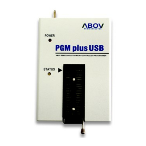
Single programmer : E-PGM+
- It programs MCU device directly.
DSDA
VDD
DSCL
VSS
RUNFLAG
Figure 1.3 E-PGM+(Single writer)

9
MC97F60128
ABOV Semiconductor Co., Ltd.
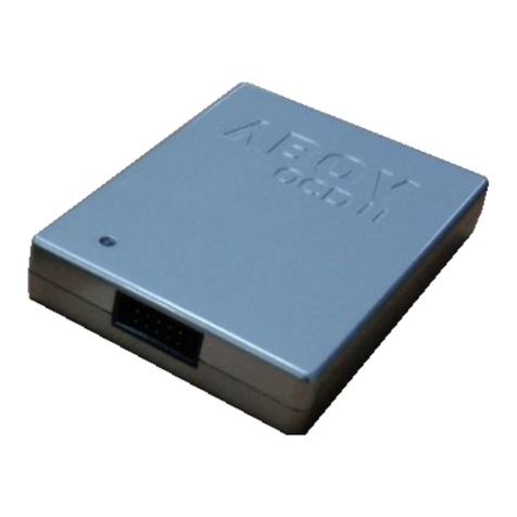
OCD emulator : OCD-II
- It can write code to MCU device too, because OCD debugger supports ISP (In System Programming).It
does not require additional H/W, except developer’s target system.
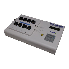
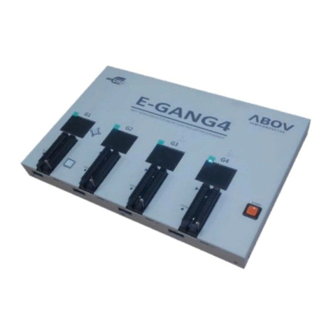
Gang programmer : E-GANG4 and E-GANG6
- It can run PC controlled mode.
- It can run standalone without PC control too.
- USB interface is supported.
- Easy to connect to the handler.
Figure 1.4 E-GANG4 and E-GANG6 (for Mass Production)

10
MC97F60128
ABOV Semiconductor Co., Ltd.
1.4 MTP programming
1.4.1 Overview
The program memory of MC97F60128 is MTP Type. This flash is accessed by serial data format. There are five
pins(DSCL, DSDA, RUNFLAG, VDD, VSS) for programming/reading the flash.
Table 1.2 Descriptions of pins which are used to programming/reading the Flash
1.4.2 On-Board programming
The MC97F60128 needs only five signal lines including VDD and VSS pins for programming FLASH with serial
protocol. Therefore the on-board programming is possible if the programming signal lines are considered when the
PCB of application board is designed.
Pin name
Main chip
pin name
During programming
I/O
Description
DSCL
P62
I
Serial clock pin. Input only pin.
DSDA
P63
I/O
Serial data pin. Output port when reading and input port when programming.
Can be assigned as input/push-pull output port.
VDD, VSS
VDD, VSS
-
Logic power supply pin.
RUNFLAG
RUNFLAG
I/O
On chip debugger run flag with a pull-down resistor.

11
MC97F60128
ABOV Semiconductor Co., Ltd.
1.4.3 Circuit Design Guide
At the FLASH programming, the programming tool needs 5 signal lines that are DSCL, DSDA, RUNFLAG, VDD and
VSS. When you design the PCB circuits, you should consider the usage of these signal lines for the on-board
programming.
Please be careful to design the related circuit of these signal pins because rising/falling timing of DSCL and DSDA is
very important for proper programming.
To application circuitDSCL(I)
DSDA(I/O) To application circuit
R2 (2kΩ~ 5kΩ)
RUNFLAG
E-PGM+, E-GANG4/E-GANG6
VDD
VSS
R1 (2kΩ~ 5kΩ)
VDD
R3
(10kΩ)R4
(10kΩ)
Option
NOTE) 1. In on-board programming mode, very high-speed signal will be provided to pin DSCL and
DSDA. And it will cause some damages to the application circuits connected to DSCL or
DSDA port if the application circuit is designed as high speed response such as relay
control circuit. If possible, the I/O configuration of DSDA, DSCL pins had better be set to
input mode.
2. The value of R1 and R2 is recommended value. It varies with circuit of system.
3. The RUNFLAG has an internal pull-down resistor(Typ 50kΩ@ 5V).
4. The DSCL and DSDA have an internal pull-up resistor(Typ 50kΩ@ 5V) during power on
or OCD mode.
5. The option is recommended if the DSCL and DSDL is not used to application circuit. This
can increase the stability of the system.
Figure 1.5 PCB design guide for on board programming

12
MC97F60128
ABOV Semiconductor Co., Ltd.
2. Block diagram
XRAM
8,192B
IRAM
256B
Flash
128KB
On-chip debug
In-system programming
Power control
Power on reset
Low voltage reset
Low voltage indicator
Power down mode
Clock generator
8MHz, Internal RC OSC
12MHz, Crystal OSC
32.768kHz, Crystal OSC
8.2MHz, PLL
LCD driver
60 segments
Buzzer
1 channel, 8-bit
UART
5 channels, 8-bit
SPI
4 channels, 8-bit
I2C
2 channels, 8-bit
CORE
M8051
General purpose I/O
20 ports normal I/O
68 ports LCD shared I/O
Watchdog timer
8 channels, 8-bit
32kHz, internal RC OSC
Basic interval timer
1 channel, 8-bit
Timer / Counter
3 channesl, 8-bit
4 channels, 16-bit
2 channels, 8-bit
or 1 channel, 16-bit
ADC
15 Input channels, 12-bit
PWM
7 channels, 8-bit
6 channels 10-bit PWM for Motor
1 channel 10-bit PWM
DAC
1 Output channel, 12-bit
FADPCM Decoder
32Kbps @8kHz
Figure 2.1 Block diagrom of MC97F60128

13
MC97F60128
ABOV Semiconductor Co., Ltd.
3. Pin assignment
MC97F60128L
(100LQFP-1414)
1
2
26
27
8
9
15
16
3
4
5
6
7
28
29
30
31
37
38
39
40
41
75
74
68
67
61
60
73
72
71
70
69
100
99
98
97
96
95
94
93
92
91
90
17
18
24
25
19
20
21
22
23
42
43
44
45
46
47
48
49
50
59
58
52
51
57
56
55
54
53
89
88
87
81
80
79
78
77
76
P00/AN0/EINT0/BLNK
P01/AN1/EINT1
P04/AN4/EINT4
P05/AN5/EINT5
P06/AN6/EINT6
P02/AN2/EINT2
P03/AN3/EINT3
RUNFLAG
AVSS
RESETB
LPF
VREG
VSS1
SXIN
SXOUT
VDD1
P17/XOUT
P16/XIN
P07/AN7/EINT7
AVREF
P62/AN8/EINT17/T7O
P64/AN10/TXD2
P63/AN9/EC7/DAC
P61/EINT18/T8O/PWM8AA
P60/SEG0/PWM8AB
P74/COM3
P73/SEG4/VLC0/PWM8CB
P72/SEG3/VLC1/PWM8CA
P71/SEG2/VLC2/PWM8BB
P70/SEG1/VLC3/PWM8BA
P65/AN11/RXD2
P77/COM0
P75/COM2
P76/COM1
P80/SEG10
P81/SEG11
P85/SEG15
P84/SEG14
P83/SEG13
P82/SEG12
P87/SEG17
P86/SEG16
P40/SEG29/EC0
PB2/SEG28
P52/SEG20/RXD3
P51/SEG19/TXD4
P54/SEG22/SS1
P53/SEG21/TXD3
P56/SEG24/TXD1/SDA1/MOSI1
P55/SEG23/SCK1
P50/SEG18/RXD4
P41/SEG30/EC1
P46/SEG35/BUZO
P45/SEG34/EINT12/T2O/PWM2O
P42/SEG31/EC2
P44/SEG33/EINT11/T1O/PWM1O
P43/SEG32/EINT10/T0O/PWM0O
P31/SEG38/TXD0/SDA0/MOSI0
P30/SEG37/SCK0
P47/SEG36/SS0
P11/SEG59/EINT14/T4O/PWM4O
P10/SEG58/EINT13/T3O/PWM3O/EXTSP2
P27/COM7/SEG52/EC4/EXTSP1
P26/COM6/SEG51/EC3/EXTSP0
P25/COM5/SEG50/TRIG
P24/COM4/SEG49/PWMOUT
P23/SEG48/(T3O/PWM3O/EXTSP2)
P13/SEG61/EINT16/T6O/PWM6O
P12/SEG60/EINT15/T5O/PWM5O
P15/SEG63/EINT9/EC6/DSDA
P14/SEG62/EINT8/EC5/DSCL
P36/SEG43/SS2/CSB2
P35/SEG42/SCK2
P20/SEG45/MOSI3
P37/SEG44/MISO3/LDACB3
P22/SEG47/SS3/CSB3
P21/SEG46/SCK3
P34/SEG41/MOSI2
P33/SEG40/MISO2/LDACB2
P32/SEG39/RXD0/SCL0/MISO0
13
14
10
11
12 63
62
66
65
64
P90/AN12/EINTA
P91/AN13/EINTB
P92/AN14/EINTC
P93/EINTD
P94/EINTE
P57/SEG25/RXD1/SCL1/MISO1
VSS2
VDD2
PB1/SEG27
PB0/SEG26
32
33
34
35
36 PA1/SEG54/EINTG
PA0/SEG53/EINTF
PA3/SEG56/EINTI
PA2/SEG55/EINTH
PA4/SEG57/EINTJ
86
85
84
83
82
PD0/SEG5
PD1/SEG6
PD4/SEG9
PD3/SEG8
PD2/SEG7
NOTE) 1. On On-Chip Debugging, ISP uses P1[5:4] pin as DSDA, DSCL.
2. The pin in parentheses can be configured by software control.
Figure 3.1 MC97F60128L 100LQFP pin assignment

14
MC97F60128
ABOV Semiconductor Co., Ltd.
MC97F68128L
(80LQFP-1212),
MC97F68128L14
(80LQFP-1414)
1
2
21
22
8
9
10
11
3
4
5
6
7
23
24
25
26
27
28
29
30
31
60
59
53
52
51
50
58
57
56
55
54
80
79
78
77
76
75
74
73
72
71
70
12
13
19
20
14
15
16
17
18
32
33
34
35
36
37
38
39
40
49
48
42
41
47
46
45
44
43
69
68
67
66
65
64
63
62
61
P00/AN0/EINT0/BLNK
P01/AN1/EINT1
P04/AN4/EINT4
P05/AN5/EINT5
P06/AN6/EINT6
P02/AN2/EINT2
P03/AN3/EINT3
RUNFLAG
AVSS
RESETB
LPF
VREG
VSS1
SXIN
SXOUT
VDD1
P17/XOUT
P16/XIN
P07/AN7/EINT7
AVREF
P11/SEG59/EINT14/T4O/PWM4O
P10/SEG58/EINT13/T3O/PWM3O/EXTSP2
P27/COM7/SEG52/EC4/EXTSP1
P26/COM6/SEG51/EC3/EXTSP0
P25/COM5/SEG50/TRIG
P24/COM4/SEG49/PWMOUT
P23/SEG48/(T3O/PWM3O/EXTSP2)
P13/SEG61/EINT16/T6O/PWM6O
P12/SEG60/EINT15/T5O/PWM5O
P15/SEG63/EINT9/EC6/DSDA
P14/SEG62/EINT8/EC5/DSCL
P36/SEG43/SS2/CSB2
P35/SEG42/SCK2
P20/SEG45/MOSI3
P37/SEG44/MISO3/LDACB3
P22/SEG47/SS3/CSB3
P21/SEG46/SCK3
P34/SEG41/MOSI2
P33/SEG40/MISO2/LDACB2
P32/SEG39/RXD0/SCL0/MISO0
P87/SEG17
P86/SEG16
P40/SEG29/EC0
P52/SEG20/RXD3
P51/SEG19/TXD4
P54/SEG22/SS1
P53/SEG21/TXD3
P56/SEG24/TXD1/SDA1/MOSI1
P55/SEG23/SCK1
P50/SEG18/RXD4
P41/SEG30/EC1
P46/SEG35/BUZO
P45/SEG34/EINT12/T2O/PWM2O
P42/SEG31/EC2
P44/SEG33/EINT11/T1O/PWM1O
P43/SEG32/EINT10/T0O/PWM0O
P31/SEG38/TXD0/SDA0/MOSI0
P30/SEG37/SCK0
P47/SEG36/SS0
P57/SEG25/RXD1/SCL1/MISO1
P62/AN8/EINT17/T7O
P64/AN10/TXD2
P63/AN9/EC7/DAC
P61/EINT18/T8O/PWM8AA
P60/SEG0/PWM8AB
P74/COM3
P73/SEG4/VLC0/PWM8CB
P72/SEG3/VLC1/PWM8CA
P71/SEG2/VLC2/PWM8BB
P70/SEG1/VLC3/PWM8BA
P65/AN11/RXD2
P77/COM0
P75/COM2
P76/COM1
P80/SEG10
P81/SEG11
P85/SEG15
P84/SEG14
P83/SEG13
P82/SEG12
NOTE) 1. On On-Chip Debugging, ISP uses P1[5:4] pin as DSDA, DSCL.
2. The P9, PA, PB and PD pins should be selected as a push-pull output or an input with
pull-up resistor by software control when the 80-pin package is used.
3. The pin in parentheses can be configured by software control.
Figure 3.2 MC97F68128L/L14 80LQFP pin assignment

15
MC97F60128
ABOV Semiconductor Co., Ltd.
MC97F67128LB14
(64LQFP-1414)
1
2
17
18
8
9
10
11
3
4
5
6
7
19
20
21
22
23
24
25
26
27
48
47
41
40
39
38
46
45
44
43
42
64
63
62
61
60
59
58
57
56
55
54
12
13
14
15
16
28
29
30
31
32
37
36
35
34
33
53
52
51
50
49
VREG
LPF
P50/SEG18/RXD4
P51/SEG19/TXD4
P00/AN0/EINT0/BLNK
P01/AN1/EINT1
P04/AN4/EINT4
P05/AN5/EINT5
P02/AN2/EINT2
P03/AN3/EINT3
RUNFLAG
AVSS
RESETB
VSS1
SXIN
SXOUT
VDD1
P17/XOUT
P16/XIN
AVREF
P11/SEG59/EINT14/T4O/PWM4O
P10/SEG58/EINT13/T3O/PWM3O/EXTSP2
P27/COM7/SEG52/EC4/EXTSP1
P26/COM6/SEG51/EC3/EXTSP0
P25/COM5/SEG50/TRIG
P24/COM4/SEG49/PWMOUT
P13/SEG61/EINT16/T6O/PWM6O
P12/SEG60/EINT15/T5O/PWM5O
P15/SEG63/EINT9/EC6/DSDA
P14/SEG62/EINT8/EC5/DSCL
P35/SEG42/SCK2
P34/SEG41/MOSI2
P33/SEG40/MISO2/LDACB2
P32/SEG39/RXD0/SCL0/MISO0
P40/SEG29/EC0
P52/SEG20/RXD3
P54/SEG22/SS1
P53/SEG21/TXD3
P56/SEG24/TXD1/SDA1/MOSI1
P55/SEG23/SCK1
P41/SEG30/EC1
P46/SEG35/BUZO
P45/SEG34/EINT12/T2O/PWM2O
P42/SEG31/EC2
P44/SEG33/EINT11/T1O/PWM1O
P43/SEG32/EINT10/T0O/PWM0O
P31/SEG38/TXD0/SDA0/MOSI0
P30/SEG37/SCK0
P47/SEG36/SS0
P57/SEG25/RXD1/SCL1/MISO1
P62/AN8/EINT17/T7O
P64/AN10/TXD2
P63/AN9/EC7/DAC
P61/EINT18/T8O/PWM8AA
P60/SEG0/PWM8AB
P74/COM3
P73/SEG4/VLC0/PWM8CB
P72/SEG3/VLC1/PWM8CA
P71/SEG2/VLC2/PWM8BB
P70/SEG1/VLC3/PWM8BA
P65/AN11/RXD2
P77/COM0
P75/COM2
P76/COM1
NOTE) 1. On On-Chip Debugging, ISP uses P1[5:4] pin as DSDA, DSCL.
2. The P06-P07, P20-P23, P36-P37, P8, P9, PA, PB and PD pins should be selected as a
push-pull output or an input with pull-up resistor by software control when the 64-pin
package is used.
3. The pin in parentheses can be configured by software control.
Figure 3.3 MC97F67128LB14 64LQFP pin assignment

16
MC97F60128
ABOV Semiconductor Co., Ltd.
MC97F66128LB14
(64LQFP-1414)
1
2
17
18
8
9
10
11
3
4
5
6
7
19
20
21
22
23
24
25
26
27
48
47
41
40
39
38
46
45
44
43
42
64
63
62
61
60
59
58
57
56
55
54
12
13
14
15
16
28
29
30
31
32
37
36
35
34
33
53
52
51
50
49
P15/SEG63/EINT9/EC6/DSDA
P14/SEG62/EINT8/EC5/DSCL
P50/SEG18/RXD4
P51/SEG19/TXD4
P00/AN0/EINT0/BLNK
P01/AN1/EINT1
P04/AN4/EINT4
P05/AN5/EINT5
P02/AN2/EINT2
P03/AN3/EINT3
P07/AN7/EINT7
AVREF
P90/AN12/EINTA
P17/XOUT
P16/XIN
VSS1
VDD1
RUNFLAG
RESETB
P06/AN6/EINT6
PA1/SEG54/EINTG
PA0/SEG53/EINTF
P27/COM7/SEG52/EC4/EXTSP1
P26/COM6/SEG51/EC3/EXTSP0
P25/COM5/SEG50/TRIG
P24/COM4/SEG49/PWMOUT
P11/SEG59/EINT14/T4O/PWM4O
P10/SEG58/EINT13/T3O/PWM3O/EXTSP2
P13/SEG61/EINT16/T6O/PWM6O
P12/SEG60/EINT15/T5O/PWM5O
P35/SEG42/SCK2
P34/SEG41/MOSI2
P33/SEG40/MISO2/LDACB2
P32/SEG39/RXD0/SCL0/MISO0
P40/SEG29/EC0
P52/SEG20/RXD3
P54/SEG22/SS1
P53/SEG21/TXD3
P56/SEG24/TXD1/SDA1/MOSI1
P55/SEG23/SCK1
P41/SEG30/EC1
P46/SEG35/BUZO
P45/SEG34/EINT12/T2O/PWM2O
P42/SEG31/EC2
P44/SEG33/EINT11/T1O/PWM1O
P43/SEG32/EINT10/T0O/PWM0O
P31/SEG38/TXD0/SDA0/MOSI0
P30/SEG37/SCK0
P47/SEG36/SS0
P57/SEG25/RXD1/SCL1/MISO1
P62/AN8/EINT17/T7O
P64/AN10/TXD2
P63/AN9/EC7/DAC
P61/EINT18/T8O/PWM8AA
P60/SEG0/PWM8AB
P74/COM3
P73/SEG4/VLC0/PWM8CB
P72/SEG3/VLC1/PWM8CA
P71/SEG2/VLC2/PWM8BB
P70/SEG1/VLC3/PWM8BA
P65/AN11/RXD2
P77/COM0
P75/COM2
P76/COM1
NOTE) 1. On On-Chip Debugging, ISP uses P1[5:4] pin as DSDA, DSCL.
2. The P20-P23, P36-P37, P8, P91-P94, PA2-PA4, PB and PD pins should be selected as a
push-pull output or an input with pull-up resistor by software control when the 64-pin
package is used.
3. The AVSS, SXIN, SXOUT, VREG and LPF pins are not in the 64-Pin package.
4. The pin in parentheses can be configured by software control.
Figure 3.4 MC97F66128LB14 64LQFP pin assignment

17
MC97F60128
ABOV Semiconductor Co., Ltd.
4. Package Diagram
Figure 4.1 100-pin LQFP-1414 Package

18
MC97F60128
ABOV Semiconductor Co., Ltd.
Figure 4.2 80-Pin LQFP-1212 Package

19
MC97F60128
ABOV Semiconductor Co., Ltd.
Figure 4.3 80-Pin LQFP-1414 Package

20
MC97F60128
ABOV Semiconductor Co., Ltd.
Figure 4.4 64-Pin LQFP-1414 Package
This manual suits for next models
5
Table of contents
Other Abov Microcontroller manuals

Abov
Abov A96G140 User manual

Abov
Abov MC96F6432S Series User manual
Abov
Abov MC95FG0128A User manual

Abov
Abov 8-bit MCU User manual

Abov
Abov MC96F6432 Series User manual

Abov
Abov MC96F8204 Series User manual

Abov
Abov EW8051 User manual

Abov
Abov A96T418GDN User manual

Abov
Abov AC33M8128L User manual

Abov
Abov MC96F6432A User manual

Abov
Abov MC80F0304 User manual

Abov
Abov A31G213CL2N User manual

Abov
Abov MC96FR116C Series User manual
Abov
Abov A31G213CLN User manual

Abov
Abov MC96FR364B User manual

Abov
Abov A31T216RLN User manual
Abov
Abov MC97F2664 User manual

Abov
Abov MC96FM204 User manual

Abov
Abov MC97F6108A User manual
Abov
Abov A96G140 User manual