Abov MC97F2664 User manual

MC97F2664
April 11, 2014 Ver. 1.4 1
ABOV SEMICONDUCTOR Co., Ltd.
8-BIT MICROCONTROLLERS
MC97F2664
User’s Manual (Ver. 1.4)

MC97F2664
2 April 11, 2014 Ver. 1.4
REVISION HISTORY
VERSION 0.0 (June 22, 2012)
VERSION 1.0 (July 24, 2012)
Change ‘±6LSB’to “ILE”in A/D CONVERTER characteristics.
Change ‘3.0V’to “Vdd @ 0.4-16MHz”in RECOMMENDED OPERATING condition.
Change ‘4.5/9.0mA (Typ/Max)‟to “IDD1 @16MHz Crystal” in DC electrical characteristics.
Change ‘4.0/8.0mA (Typ/Max)‟to “IDD1 @16MHz IRC” in DC electrical characteristics.
Change ‘2.0/4.0mA (Typ/Max)‟to “IDD2 @16MHz Crystal” in DC electrical characteristics.
Change ‘1.0/2.0mA (Typ/Max)‟to “IDD2 @12MHz Crystal” in DC electrical characteristics.
Change ‘1.2/2.4mA (Typ/Max)‟to “IDD2 @16MHz IRC” in DC electrical characteristics.
Change ‘1.60/1.79V (Typ/Max)‟to “VLVR, VLVI” in LVR and LVI characteristics.
Change Figure 10.6 Effective Timing of Interrupt
Change Figure 14.1 Block Diagram of On-Chip Debug System
Change Figure 1.1 Connection of Transmission
Remove 42 PIN DIP package
Remove INTERRUPT GROUP PRIORITY LEVEL at INTERRUPT CONTROLLER
Remove Appendix B
Add 64 PIN LQFP-1414 package
Add RUNFLAG Pull-Down Resistor(RPD) in DC electrical characteristics.
VERSION 1.1 (October 4, 2012)
Modify Figure 7.17 Recommended Circuit and Layout
Add Figure 7.18 Recommended Circuit and Layout with SMPS Power
VERSION 1.2 (January 11, 2013)
Add 0.1uF Bypass capacitor in Internal RC Oscillator characteristics
Change ‘14/24mA, 10/18mA’to LVR/LVI current in LVR/LVI electrical characteristics.
Change ‘±5LSB’to “ZOE”in A/D CONVERTER characteristics
Change ‘±5LSB’to “FSE”in A/D CONVERTER characteristics
Change ‘10,000/100,000 times‘to Endurance of Write/Erase in internal flash rom characteristics.
VERSION 1.3 (March 18, 2014)
Add 64 PIN QFN package, MC97F2664UB
AVREF range changed from 1.8V~VDD to 2.7V~VDD
Figure 10.3 modified
Add contents, “Writing “1” has no effect” in all interrupt flag bits.
Appendix 1 “DJNZ Rn,rel” instruction 3bytes 2bytes
VERSION 1.4 (March 18, 2014) This Book
AVREF range changed from 2.7V~VDD to 1.8V~VDD
Version 1.4
Published by FAE Team
2014 ABOV Semiconductor Co.,Ltd. All rights reserved.
Additional information of this manual may be served by ABOV Semiconductor offices in Korea or Distributors.
ABOV Semiconductor reserves the right to make changes to any information here in at any time without notice.
The information, diagrams and other data in this manual are correct and reliable; however, ABOV
Semiconductor is in no way responsible for any violations of patents or other rights of the third party
generated by the use of this manual.

MC97F2664
April 11, 2014 Ver. 1.4 3
Table of Contents
1. Overview...........................................................................................................................................................10
1.1 Description .................................................................................................................................................10
1.2 Features.....................................................................................................................................................11
1.3 Ordering Information ..................................................................................................................................12
1.4 Development Tools ....................................................................................................................................13
2. Block Diagram...................................................................................................................................................15
3. Pin Assignment.................................................................................................................................................16
4. Package Diagram..............................................................................................................................................20
5. Pin Description..................................................................................................................................................24
6. Port Structures..................................................................................................................................................29
6.1 General Purpose I/O Port...........................................................................................................................29
6.2 External Interrupt I/O Port...........................................................................................................................30
7. Electrical Characteristics...................................................................................................................................31
7.1 Absolute Maximum Ratings........................................................................................................................31
7.2 Recommended Operating Conditions ........................................................................................................31
7.3 A/D Converter Characteristics....................................................................................................................32
7.4 Power-On Reset Characteristics................................................................................................................33
7.5 Low Voltage Reset and Low Voltage Indicator Characteristics ..................................................................33
7.6 Internal RC Oscillator Characteristics.........................................................................................................34
7.7 Internal Watch-Dog Timer RC Oscillator Characteristics............................................................................34
7.8 DC Characteristics .....................................................................................................................................35
7.9 AC Characteristics......................................................................................................................................37
7.10 SPI Characteristics...................................................................................................................................38
7.11 UART Characteristics...............................................................................................................................39
7.12 I2C Characteristics...................................................................................................................................40
7.13 Data Retention Voltage in Stop Mode ......................................................................................................41
7.14 Internal Flash Rom Characteristics ..........................................................................................................42
7.15 Input/Output Capacitance.........................................................................................................................42
7.16 Main Clock Oscillator Characteristics.......................................................................................................43
7.17 Sub Clock Oscillator Characteristics ........................................................................................................44
7.18 Main Oscillation Stabilization Characteristics ...........................................................................................45
7.19 Sub Oscillation Characteristics.................................................................................................................45
7.20 Operating Voltage Range.........................................................................................................................46
7.21 Recommended Circuit and Layout...........................................................................................................47
7.22 Recommended Circuit and Layout with SMPS Power..............................................................................48
7.23 Typical Characteristics .............................................................................................................................49
8. Memory.............................................................................................................................................................52
8.1 Program Memory........................................................................................................................................52
8.2 Data Memory..............................................................................................................................................54
8.3 XRAM Memory...........................................................................................................................................56
8.4 SFR Map....................................................................................................................................................57
9. I/O Ports............................................................................................................................................................70
9.1 I/O Ports.....................................................................................................................................................70
9.2 Port Register ..............................................................................................................................................70
9.3 P0 Port .......................................................................................................................................................73
9.4 P1 Port .......................................................................................................................................................75
9.5 P2 Port .......................................................................................................................................................78
9.6 P3 Port .......................................................................................................................................................81
9.7 P4 Port .......................................................................................................................................................84
9.8 P5 Port .......................................................................................................................................................86

MC97F2664
4 April 11, 2014 Ver. 1.4
9.9 P6 Port .......................................................................................................................................................88
9.10 P7 Port .....................................................................................................................................................90
10. Interrupt Controller..........................................................................................................................................92
10.1 Overview ..................................................................................................................................................92
10.2 External Interrupt......................................................................................................................................93
10.3 Block Diagram..........................................................................................................................................94
10.4 Interrupt Vector Table...............................................................................................................................95
10.5 Interrupt Sequence...................................................................................................................................96
10.6 Effective Timing after Controlling Interrupt Bit..........................................................................................97
10.7 Multi Interrupt ...........................................................................................................................................98
10.8 Interrupt Enable Accept Timing ................................................................................................................99
10.9 Interrupt Service Routine Address............................................................................................................99
10.10 Saving/Restore General-Purpose Registers...........................................................................................99
10.11 Interrupt Timing ....................................................................................................................................100
10.12 Interrupt Register Overview..................................................................................................................100
10.13 Interrupt Register Description...............................................................................................................102
11. Peripheral Hardware .....................................................................................................................................112
11.1 Clock Generator.....................................................................................................................................112
11.2 Basic Interval Timer................................................................................................................................115
11.3 Watch Dog Timer ...................................................................................................................................118
11.4 Watch Timer...........................................................................................................................................121
11.5 Timer 0/1/2/3..........................................................................................................................................124
11.6 Timer 4/5................................................................................................................................................135
11.7 Timer 6/7/8/9..........................................................................................................................................145
11.8 Buzzer Driver..........................................................................................................................................156
11.9 SPI 2/3....................................................................................................................................................159
11.10 UART2/3/4............................................................................................................................................165
11.11 USI0/1 (UART + SPI + I2C)..................................................................................................................179
11.12 Baud Rate setting (example)................................................................................................................216
11.13 12-Bit A/D Converter............................................................................................................................217
12. Power Down Operation.................................................................................................................................224
12.1 Overview ................................................................................................................................................224
12.2 Peripheral Operation in IDLE/STOP Mode.............................................................................................224
12.3 IDLE Mode .............................................................................................................................................225
12.4 STOP Mode............................................................................................................................................226
12.5 Release Operation of STOP Mode.........................................................................................................227
13. RESET..........................................................................................................................................................229
13.1 Overview ................................................................................................................................................229
13.2 Reset Source..........................................................................................................................................229
13.3 RESET Block Diagram...........................................................................................................................229
13.4 RESET Noise Canceller.........................................................................................................................230
13.5 Power on RESET...................................................................................................................................230
13.6 External RESETB Input..........................................................................................................................233
13.7 Brown Out Detector Processor...............................................................................................................234
13.8 LVI Block Diagram..................................................................................................................................235
14. On-chip Debug System.................................................................................................................................239
14.1 Overview ................................................................................................................................................239
14.2 Two-Pin External Interface.....................................................................................................................240
15. Flash Memory ...............................................................................................................................................245
15.1 Overview ................................................................................................................................................245
16. Configure Option...........................................................................................................................................256
16.1 Configure Option Control........................................................................................................................256
17. APPENDIX....................................................................................................................................................257

MC97F2664
April 11, 2014 Ver. 1.4 5
List of Figures
Figure 1.1 OCD2 Debugger and Pin Description....................................................................................13
Figure 1.2 PGMplusUSB (Single Writer).................................................................................................14
Figure 1.3 StandAlone PGMplus (Single Writer).....................................................................................14
Figure 1.4 StandAlone Gang8 (for Mass Production) .............................................................................14
Figure 2.1 Block Diagram .......................................................................................................................15
Figure 3.1 MC97F2664L 64LQFP-1010 Pin Assignment........................................................................16
Figure 3.2 MC97F2664L14 64LQFP-1414 Pin Assignment....................................................................17
Figure 3.1 MC97F2664UB 64QFN Pin Assignment................................................................................18
Figure 3.3 MC97F2464 44MQFP-1010 Pin Assignment.........................................................................19
Figure 4.1 64-Pin LQFP-1010 Package..................................................................................................20
Figure 4.2 64-Pin LQFP-1414 Package..................................................................................................21
Figure 4.3 64-Pin QFN Package.............................................................................................................22
Figure 4.4 44-Pin MQFP-1010 Package.................................................................................................23
Figure 6.1 General Purpose I/O Port ......................................................................................................29
Figure 6.2 External Interrupt I/O Port......................................................................................................30
Figure 7.1 Input Timing for RESETB ......................................................................................................37
Figure 7.2 Input Timing for External Interrupts........................................................................................37
Figure 7.3 Input Timing for EC0 –EC9...................................................................................................37
Figure 7.4 SPI Timing.............................................................................................................................38
Figure 7.5 Waveform for UART Timing Characteristics..........................................................................39
Figure 7.6 Timing Waveform for the UART Module................................................................................39
Figure 7.7 I2C Timing .............................................................................................................................40
Figure 7.8 Stop Mode Release Timing when Initiated by an Interrupt ....................................................41
Figure 7.9 Stop Mode Release Timing when Initiated by RESETB ........................................................41
Figure 7.10 Crystal/Ceramic Oscillator ...................................................................................................43
Figure 7.11 External Clock......................................................................................................................43
Figure 7.12 Crystal Oscillator..................................................................................................................44
Figure 7.13 External Clock......................................................................................................................44
Figure 7.14 Clock Timing Measurement at XIN ......................................................................................45
Figure 7.15 Clock Timing Measurement at SXIN....................................................................................45
Figure 7.16 Operating Voltage Range ....................................................................................................46
Figure 7.17 Recommended Circuit and Layout.......................................................................................47
Figure 7.18 Recommended Circuit and Layout with SMPS Power.........................................................48
Figure 7.19 RUN (IDD1) Current ............................................................................................................49
Figure 7.20 IDLE (IDD2) Current............................................................................................................49
Figure 7.21 SUB RUN (IDD3) Current....................................................................................................50
Figure 7.22 SUB IDLE (IDD4) Current....................................................................................................50
Figure 7.23 STOP (IDD5) Current ..........................................................................................................51
Figure 8.1 Program Memory...................................................................................................................53
Figure 8.2 Data Memory Map .................................................................................................................54
Figure 8.3 Lower 128 Bytes RAM...........................................................................................................55
Figure 8.4 XDATA Memory Area ............................................................................................................56
Figure 10.1 External Interrupt Description ..............................................................................................93
Figure 10.2 Block Diagram of Interrupt...................................................................................................94
Figure 10.3 Interrupt Vector Address Table............................................................................................96
Figure 10.4 Effective Timing of Interrupt Enable Register......................................................................97

MC97F2664
6 April 11, 2014 Ver. 1.4
Figure 10.5 Effective Timing of Interrupt Flag Register...........................................................................97
Figure 10.6 Effective Timing of Interrupt.................................................................................................98
Figure 10.7 Interrupt Response Timing Diagram....................................................................................99
Figure 10.8 Correspondence between Vector Table Address and the Entry Address of ISP .................99
Figure 10.9 Saving/Restore Process Diagram and Sample Source .......................................................99
Figure 10.10 Timing Chart of Interrupt Acceptance and Interrupt Return Instruction............................100
Figure 11.1 Clock Generator Block Diagram ........................................................................................112
Figure 11.2 Basic Interval Timer Block Diagram...................................................................................115
Figure 11.3 Watch Dog Timer Interrupt Timing Waveform....................................................................118
Figure 11.4 Watch Dog Timer Block Diagram.......................................................................................119
Figure 11.5 Watch Timer Block Diagram..............................................................................................121
Figure 11.6 8-Bit Timer/Counter Mode for Timer 0/1/2/3 (Where n = 0, 1, 2, and 3).............................125
Figure 11.7 8-Bit Timer/Counter 0/1/2/3 Example (Where n = 0, 1, 2, and 3).......................................125
Figure 11.8 8-Bit PWM Mode for Timer 0/1/2/3 (Where n = 0, 1, 2, and 3)...........................................126
Figure 11.9 PWM Output Waveforms in PWM Mode for Timer 0/1/2 (Where n = 0, 1, 2, and 3)..........127
Figure 11.10 8-Bit Capture Mode for Timer 0/1/2/3 (Where n = 0, 1, 2, and 3).....................................128
Figure 11.11 Input Capture Mode Operation for Timer 0/1/2/3 (Where n = 0, 1, 2, and 3) ...................129
Figure 11.12 Express Timer Overflow in Capture Mode (Where n = 0, 1, 2, and 3) .............................129
Figure 11.13 8-Bit Timer 0/1/2/3 Block Diagram (Where n = 0, 1, 2, and 3) .........................................130
Figure 11.14 16-Bit Timer/Counter Mode for Timer 4/5 ( where n= 4 and 5) ........................................136
Figure 11.15 16-Bit Timer/Counter 4/5 Example ( where n= 4 and 5)...................................................136
Figure 11.16 16-Bit Capture Mode for Timer 4/5 ( where n= 4 and 5) ..................................................137
Figure 11.17 Input Capture Mode Operation for Timer 4/5 ( where n= 4 and 5)...................................138
Figure 11.18 Express Timer Overflow in Capture Mode ( where n= 4 and 5).......................................138
Figure 11.19 16-Bit PPG Mode for Timer 4/5 ( where n= 4 and 5)........................................................139
Figure 11.20 16-Bit PPG Mode Timming chart for Timer 4/5 ( where n= 4 and 5)................................140
Figure 11.21 16-Bit Timer 4/5 Block Diagram ( where n= 4 and 5).......................................................141
Figure 11.22 16-Bit Timer/Counter Mode for Timer 6/7/8/9 ( where n= 6,7,8, and 9) ...........................146
Figure 11.23 16-Bit Timer/Counter 6/7/8/9 Example ( where n= 6,7,8,and 9).......................................146
Figure 11.24 16-Bit Capture Mode for Timer 6/7/8/9 ( where n= 6,7,8, and 9) .....................................147
Figure 11.25 Input Capture Mode Operation for Timer 6/7/8/9 ( where n= 6,7,8, and 9).....................148
Figure 11.26 Express Timer Overflow in Capture Mode ( where n= 6,7,8, and 9)................................148
Figure 11.27 16-Bit PPG Mode for Timer 6/7/8/9 ( where n= 6,7,8, and 9)...........................................149
Figure 11.28 16-Bit PPG Mode Timming chart for Timer 6/7/8/9 ( where n= 6,7,8, and 9)...................150
Figure 11.29 16-Bit Timer 6/7/8/9 Block Diagram ( where n= 6,7,8, and 9)..........................................151
Figure 11.30 Buzzer Driver Block Diagram...........................................................................................156
Figure 11.31 SPI 2/3 Block Diagram (where n = 2 and 3).....................................................................159
Figure 11.32 SPI 2/3 Transmit/Receive Timing Diagram at CPHA = 0 (Where n = 2 and 3) ................161
Figure 11.33 SPI 2/3 Transmit/Receive Timing Diagram at CPHA = 1 (Where n = 2 and 3) ................161
Figure 11.34 UART Block Diagram(where n = 2,3, and 4)....................................................................166
Figure 11.35 Clock Generation Block Diagram (where n = 2,3, and 4).................................................167
Figure 11.36 Frame Format..................................................................................................................168
Figure 11.37 Start Bit Sampling (where n = 2,3, and 4)........................................................................172
Figure 11.38 Sampling of Data and Parity Bit (where n = 2,3, and 4)..................................................172
Figure 11.39 Stop Bit Sampling and Next Start Bit Sampling (where n = 2,3, and 4) ...........................173
Figure 11.40 USI0/1 UART Block Diagram (Where n = 0 and 1)..........................................................181
Figure 11.41 Clock Generation Block Diagram (USIn, where n = 0 and 1)...........................................182
Figure 11.42 Synchronous Mode SCKn Timing (USIn , where n = 0 and 1).........................................183
Figure 11.43 Frame Format (USI0/1)....................................................................................................184

MC97F2664
April 11, 2014 Ver. 1.4 7
Figure 11.44 Asynchronous Start Bit Sampling (USIn, where n = 0 and 1) ..........................................188
Figure 11.45 Asynchronous Sampling of Data and Parity Bit (USIn, where n = 0 and 1) .....................188
Figure 11.46 Stop Bit Sampling and Next Start Bit Sampling (USIn, where n = 0 and 1) .....................189
Figure 11.47 USI0/1 SPI Clock Formats when CPHAn=0 (where n = 0 and 1) ....................................191
Figure 11.48 USI0/1 SPI Clock Formats when CPHAn=1 (where n = 0 and 1) ....................................192
Figure 11.49 USI0/1 SPI Block Diagram (where n = 0 and 1)...............................................................193
Figure 11.50 Bit Transfer on the I2C-Bus (USIn, where n = 0 and 1) ...................................................194
Figure 11.51 START and STOP Condition (USIn, where n = 0 and 1).................................................195
Figure 11.52 Data Transfer on the I2C-Bus (USIn, where n = 0 and 1)................................................195
Figure 11.53 Acknowledge on the I2C-Bus (USIn, where n = 0 and 1).................................................196
Figure 11.54 Clock Synchronization during Arbitration Procedure (USIn, where n = 0 and 1)..............197
Figure 11.55 Arbitration Procedure of Two Masters (USIn, where n = 0 and 1) ...................................197
Figure 11.56 Formats and States in the Master Transmitter Mode (USIn, where n = 0 and 1).............199
Figure 11.57 Formats and States in the Master Receiver Mode (USIn, where n = 0 and 1).................201
Figure 11.58 Formats and States in the Slave Transmitter Mode (USIn, where n = 0 and 1)...............203
Figure 11.59 Formats and States in the Slave Receiver Mode (USIn, where n = 0 and 1)...................205
Figure 11.60 USI0/1 I2C Block Diagram (where n = 0 and 1)...............................................................206
Figure 11.61 12-bit ADC Block Diagram...............................................................................................218
Figure 11.62 A/D Analog Input Pin with Capacitor................................................................................218
Figure 11.63 A/D Power (AVREF) Pin with Capacitor...........................................................................218
Figure 11.64 ADC Operation for Align Bit.............................................................................................219
Figure 11.65 A/D Converter Operation Flow.........................................................................................220
Figure 12.1 IDLE Mode Release Timing by External Interrupt..............................................................225
Figure 12.2 STOP Mode Release Timing by External Interrupt............................................................226
Figure 12.3 STOP Mode Release Flow ................................................................................................227
Figure 13.1 RESET Block Diagram ......................................................................................................229
Figure 13.2 Reset noise canceller timer diagram..................................................................................230
Figure 13.3 Fast VDD Rising Time .......................................................................................................230
Figure 13.4 Internal RESET Release Timing On Power-Up .................................................................230
Figure 13.5 Configuration Timing when Power-on................................................................................231
Figure 13.6 Boot Process WaveForm...................................................................................................231
Figure 13.7 Timing Diagram after RESET ............................................................................................233
Figure 13.8 Oscillator generating waveform example...........................................................................233
Figure 13.9 Block Diagram of BOD.......................................................................................................234
Figure 13.10 Internal Reset at the power fail situation..........................................................................234
Figure 13.11 Configuration timing when BOD RESET..........................................................................235
Figure 13.12 LVI Diagram.....................................................................................................................235
Figure 14.1 Block Diagram of On-Chip Debug System.........................................................................239
Figure 14.2 10-bit Transmission Packet................................................................................................240
Figure 14.3 Data Transfer on the Twin Bus..........................................................................................241
Figure 14.4 Bit Transfer on the Serial Bus............................................................................................241
Figure 14.5 Start and Stop Condition....................................................................................................242
Figure 14.6 Acknowledge on the Serial Bus.........................................................................................242
Figure 14.7 Clock Synchronization during Wait Procedure...................................................................243
Figure 14.8 Connection of Transmission ..............................................................................................244
Figure 15.1 Flash Program ROM Structure ..........................................................................................246

MC97F2664
8 April 11, 2014 Ver. 1.4
List of Tables
Table 1-1 Ordering Information of MC97F2664 ......................................................................................12
Table 5-1 Normal Pin Description...........................................................................................................24
Table 7-1 Absolute Maximum Ratings....................................................................................................31
Table 7-2 Recommended Operating Conditions.....................................................................................31
Table 7-3 A/D Converter Characteristics ................................................................................................32
Table 7-4 Power-on Reset Characteristics .............................................................................................33
Table 7-5 LVR and LVI Characteristics...................................................................................................33
Table 7-6 High Internal RC Oscillator Characteristics.............................................................................34
Table 7-7 Internal WDTRC Oscillator Characteristics.............................................................................34
Table 7-8 DC Characteristics..................................................................................................................35
Table 7-9 AC Characteristics..................................................................................................................37
Table 7-10 SPI Characteristics...............................................................................................................38
Table 7-11 UART Characteristics ...........................................................................................................39
Table 7-12 I2C Characteristics ...............................................................................................................40
Table 7-13 Data Retention Voltage in Stop Mode...................................................................................41
Table 7-14 Internal Flash Rom Characteristics.......................................................................................42
Table 7-15 Input/Output Capacitance.....................................................................................................42
Table 7-16 Main Clock Oscillator Characteristics ...................................................................................43
Table 7-17 Sub Clock Oscillator Characteristics.....................................................................................44
Table 7-18 Main Oscillation Stabilization Characteristics........................................................................45
Table 7-19 Sub Oscillation Stabilization Characteristics.........................................................................45
Table 8-1 SFR Map Summary................................................................................................................57
Table 8-2 Extended SFR Map Summary................................................................................................58
Table 8-3 SFR Map.................................................................................................................................59
Table 8-4 Extended SFR Map ................................................................................................................63
Table 9-1 Port Register Map...................................................................................................................71
Table 10-1 Interrupt Vector Address Table.............................................................................................95
Table 10-2 Interrupt Register Map........................................................................................................102
Table 11-1 Clock Generator Register Map ...........................................................................................113
Table 11-2 Basic Interval Timer Register Map......................................................................................116
Table 11-3 Watch Dog Timer Register Map..........................................................................................119
Table 11-4 Watch Timer Register Map.................................................................................................122
Table 11-5 Timer 0/1/2 Operating Modes.............................................................................................124
Table 11-6 Timer 0/1/2/3 Register Map ................................................................................................131
Table 11-7 Timer 4/5 Operating Modes................................................................................................135
Table 11-8 Timer 2 Register Map .........................................................................................................141
Table 11-9 Timer 6/7/8/9 Operating Modes..........................................................................................145
Table 11-10 Timer 2 Register Map .......................................................................................................151
Table 11-11 Buzzer Frequency at fBUZ= 2 MHz.................................................................................156
Table 11-12 Buzzer Driver Register Map..............................................................................................157
Table 11-13 SPI 2/3 Register Map........................................................................................................162
Table 11-14 Equations for Calculating Baud Rate Register Setting......................................................167
Table 11-15 UART Register Map (where n = 2,3, and 4)......................................................................173
Table 11-16 Examples of UARTnBD Settings for Commonly Used Oscillator Frequencies .................178
Table 11-17 Equations for Calculating USI0/1 Baud Rate Register Setting..........................................182

MC97F2664
April 11, 2014 Ver. 1.4 9
Table 11-18 CPOLn Functionality (where n = 0 and 1).........................................................................190
Table 11-19 USI0/1 Register Map (where n = 0 and 1) ........................................................................207
Table 11-20 Examples of USI0BD and USI1BD Settings for Commonly Used Oscillator Frequencies 216
Table 11-21 ADC Register Map............................................................................................................220
Table 12-1 Peripheral Operation during Power Down Mode.................................................................224
Table 12-2 Power Down Operation Register Map ...............................................................................228
Table 13-1 Reset State.........................................................................................................................229
Table 13-2 Boot Process Description....................................................................................................232
Table 13-3 Reset Operation Register Map ...........................................................................................236
Table 15-1 Flash Memory Register Map...............................................................................................247

MC97F2664
10 April 11, 2014 Ver. 1.4
MC97F2664
CMOS SINGLE-CHIP 8-BIT MICROCONTROLLER
WITH 12-BIT A/D CONVERTER
1. Overview
1.1 Description
The MC97F2664 is advanced CMOS 8-bit microcontroller with 64k bytes of FLASH. This is powerful
microcontroller which provides a highly flexible and cost effective solution to many embedded control applications.
This provides the following features : 64k bytes of FLASH, 256 bytes of IRAM, 4,096 bytes of XRAM , general
purpose I/O, basic interval timer, watchdog timer, 8/16-bit timer/counter, 16-bit PPG output, 8-bit PWM output,
watch timer, buzzer driving port, SPI, UART, I2C, 12-bit A/D converter, on-chip POR, LVR, LVI, on-chip oscillator
and clock circuitry. The MC97F2664 also supports power saving modes to reduce power consumption.
Device Name
FLASH
XRAM
IRAM
ADC
I/O PORT
Package
MC97F2664L
MC97F2664L14
MC97F2664UB
MC97F2464Q
64k bytes
4,096 bytes
256 bytes
15 channel
15 channel
15 channel
10 channel
61
61
61
41
64 LQFP-1010
64 LQFP-1414
64 QFN
44 MQFP-1010

MC97F2664
April 11, 2014 Ver. 1.4 11
1.2 Features
•CPU
- 8 Bit CISC Core (8051 Compatible)
•ROM (FLASH) Capacity
-64k Bytes
-Flash with self read/write capability
- On chip debug and In-system programming (ISP)
-Endurance : 10,000 times (Sector 0~1019)
100,000 times (Sector 1020~1023)
•256 Bytes IRAM
•4,096 Bytes XRAM
•General Purpose I/O (GPIO)
- Normal I/O : 61 Ports
(P0, P1,P2,P3,P4,P5,P6,P7[4:0])
•Basic Interval Timer (BIT)
- 8Bit × 1ch
- Watch Dog Timer (WDT)
- 8Bit × 1ch
- 5kHz internal RC oscillator
•Timer/ Counter
- 8Bit × 4ch (T0/T1/T2/T3)
- 16Bit × 6ch (T4/T5/T6/T7/T8/T9)
•Programmable Pulse Generation
- 8Bit PWM (by T0/T1/T2/T3)
- Pulse generation (by T4/T5/T6/T7/T8/T9)
•Watch Timer (WT)
- 3.91ms/0.25s/0.5s/1s/1m interval at 32.768kHz
•Buzzer
- 8Bit × 1ch
•SPI
- 8Bit × 2ch
•UART
- 8Bit × 3ch
•USI (UART + SPI + I2C)
- 8Bit UART × 2ch, 8Bit SPI × 2ch, and I2C × 2ch
•12 Bit A/D Converter
- 15 Input channels
•Power On Reset
- Reset release level (1.4V)
•Low Voltage Reset
- 14 level detect (1.60V/ 2.00V/ 2.10V/ 2.20V/
2.32V/ 2.44V/ 2.59V/ 2.75V/ 2.93V/ 3.14V/
3.38V/ 3.67V/ 4.00V/ 4.40V)
•Low Voltage Indicator
- 13 level detect (2.00V/ 2.10V/ 2.20V/ 2.32V/
2.44V/ 2.59V/ 2.75V/ 2.93V/ 3.14V/ 3.38V/
3.67V/ 4.00V/ 4.40V)
•Interrupt Sources
- External Interrupts
(EINT0~A, EINT10~19) (21)
- Timer(0/1/2/3/4/5/6/7/8/9) (14)
- WDT (1)
- BIT (1)
- WT (1)
- SPI 2/3 (2)
- UART 2/3/4 (6)
- USI0/1 (4)
- ADC (1)
- Stack OVF(1)
•Internal RC Oscillator
- Internal RC frequency:
16MHz ±1.5% (TA= 0 ~ +50°C)
•Power Down Mode
- STOP, IDLE mode
•Operating Voltage and Frequency
- 1.8V ~ 5.5V (@32 ~ 38kHz with X-tal)
- 1.8V ~ 5.5V (@0.4 ~ 4.2MHz with X-tal)
- 2.7V ~ 5.5V (@0.4 ~ 12.0MHz with X-tal)
- 3.0V ~ 5.5V (@0.4 ~ 16.0MHz with X-tal)
- 1.8V ~ 5.5V (@0.5 ~ 8.0MHz with Internal RC)
- 2.0V ~ 5.5V (@0.5 ~ 16.0MHz with Internal RC)
- Voltage dropout converter included for core
•Minimum Instruction Execution Time
- 125nS (@ 16MHz main clock)
- 61μs (@t 32.768kHz sub clock)
•Operating Temperature: –40 ~ + 85℃
•Oscillator Type
- 0.4-16MHz Crystal or Ceramic for main clock
- 32.768kHz Crystal for sub clock
•Package Type
- 64 LQFP-1010
- 64 LQFP-1414
- 64 QFN
- 44 MQFP-1010
- Pb-free package

MC97F2664
12 April 11, 2014 Ver. 1.4
1.3 Ordering Information
Table 1-1 Ordering Information of MC97F2664
Device name
ROM size
IRAM size
XRAM size
Package
MC97F2664L
64k bytes FLASH
256 bytes
4,096 bytes
64 LQFP-1010
MC97F2664L14
64 LQFP-1414
MC97F2664UB
64 QFN
MC97F2464Q
44 MQFP-1010

MC97F2664
April 11, 2014 Ver. 1.4 13
1.4 Development Tools
1.4.1 Compiler
We do not provide the compiler. Please contact the third parties.
The core of MC97F2664 is Mentor 8051. And, device ROM size is smaller than 64k bytes. Developer can use all
kinds of third party’s standard 8051 compiler.
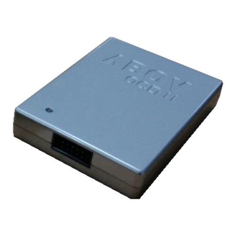
1.4.2 OCD2 emulator and debugger
The OCD2 (On Chip Debug 2) emulator supports ABOV Semiconductor’s 8051 series MCU emulation.
The OCD2 interface uses two-wire interfacing between PC and MCU which is attached to user’s system. The
OCD2 can read or change the value of MCU internal memory and I/O peripherals. And the OCD2 also controls
MCU internal debugging logic, it means OCD2 controls emulation, step run, monitoring, etc.
The OCD2 Debugger program works on Microsoft-Windows NT, 2000, XP, Vista (32bit), 7 operating system.
If you want to see more details, please refer to OCD2 debugger manual. You can download debugger S/W and
manual from our web-site.
Connection:
- DSCL (MC97F2664 P62 port)
- DSDA (MC97F2664 P63 port)
- RTIME (MC97F2664 RUNFLAG port, Option)
NOTE) MC97F2664 Use Only OCD2.
OCD2 connector diagram: Connect OCD2 with user system
Figure 1.1 OCD2 Debugger and Pin Description
2
User VCC
1
3
4
5
6
7
8
10
9
User GND
DSCL
DSDA
RTIME

MC97F2664
14 April 11, 2014 Ver. 1.4
1.4.3 Programmer
Single programmer:
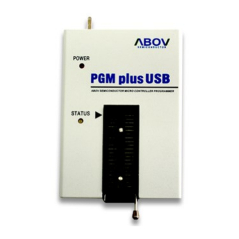
PGMplus USB: It programs MCU device directly.
Figure 1.2 PGMplusUSB (Single Writer)
StandAlone PGMplus: It programs MCU device directly.
Figure 1.3 StandAlone PGMplus (Single Writer)
OCD emulator: It can write code in MCU device too, because OCD debugging supports ISP (In System
Programming).
It does not require additional H/W, except developer’s target system.
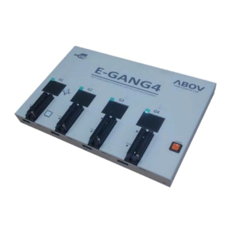
Gang programmer:
It programs 8 MCU devices at once.
So, it is mainly used in mass production line.
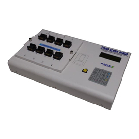
Gang programmer is standalone type, it means it does not require host PC, after a program is
downloaded from host PC to Gang programmer.
Figure 1.4 StandAlone Gang8 (for Mass Production)

MC97F2664
April 11, 2014 Ver. 1.4 15
2. Block Diagram
VDD VSS
M8051 Core
IRAM
(256 Bytes)
8-Bit Timer 0
64K Bytes Flash
T0O/PWM0O/P50
EINT10/P50
EC0/P54
P61/SCK0
P62/RXD0/SCL0/MISO0/DSCL
P63/TXD0/SDA0/MOSI0/DSDA
Watch Timer
MOSI3/P70
MISO3/P71
SCK3/P72
SPI3 SS3/P73
Buzzer BUZO/P33
XRAM
(4k Bytes)
8-Bit Timer 1
T1O/PWM1O/P51
EINT11/P51
EC1/P55
8-Bit Timer 2
T2O/PWM2O/P52
EINT12/P52
EC2/P56
P0 Port
P00/AVREF
P01-P07/AN8-AN14
USI0
UART0
SPI0
I2C0
TXD0/P63
RXD0/P62
MOSI0/P63
MISO0/P62
SCK0/P61
SS0/P60
SDA0/P63
SCL0/P62
TXD1/P40
RXD1/P41
MOSI1/P40
MISO1/P41
SCK1/P42
SS1/P43
SDA1/P40
SCL1/P41
Watchdog Timer
5KHz INT-RC OSC
Basic Interval Timer
Power On Reset
Low Voltage Reset
P6 Port
P60/SS0
Low Voltage
Indicator
USI1
UART1
SPI1
I2C1
On-Chip Debug
DSDA DSCL
INT-RC OSC
16MHz
Voltage
Down
Converter
RESETB
SXOUT
SXIN
XIN
XOUT
CLOCK/SYSTEM
CONTROL
P64/XOUT
P65/XIN
P66/SXIN
AN0-AN7/P10-P17
AN8-AN14/P01-P07 12-Bit A/D Converter
8-Bit Timer 3
T3O/PWM3O/P53
EINT13/P53
EC3/P57
16-Bit Timer 4
T4O/PWM4O/P30
EINT14/P30
EC4/P72
16-Bit Timer 5
T5O/PWM5O/P31
EINT15/P31
EC5/P73
UART2 TXD2/P44
RXD2/P45
P2 Port
P20/EINT17/T7O/PWM7O
P21/EINT18/T8O/PWM8O
P22/EINT19/T9O/PWM9O
P23/TXD4
P3 Port
P30/EINT14/T4O/PWM4O
P31/EINT15/T5O/PWM5O
P32/EINT16/T6O/PWM6O
P33/BUZO/(EC6)
P34/MOSI2
P35/MISO2/EC7
P36/SCK2/EC8
P37/SS2/EC9
16-Bit Timer 6
T6O/PWM6O/P32
EINT16/P32
EC6/P74/(P33)
UART3 TXD3/P46
RXD3/P47
UART4 TXD4/P23
RXD4/P24
MOSI2/P34
MISO2/P35
SCK2/P36
SPI2 SS2/P37
P1 PortP10-P17/AN0-AN7/EINT0-EINT7
P24/RXD4
P25/EINT8
P26/EINT9
P27/EINTA
P71/MISO3
P72/SCK3/EC4
P73/SS3/EC5
P7 Port
P70/MOSI3
P74/EC6
P51/EINT11/T1O/PWM1O
P52/EINT12/T2O/PWM2O
P53/EINT13/T3O/PWM3O
P5 Port
P50/EINT10/T0O/PWM0O
P54/EC0
P55/EC1
P56/EC2
P57/EC3/RESETB
AVREF/P00
16-Bit Timer 7
T7O/PWM7O/P20
EINT17/P20
EC7/P35
16-Bit Timer 8
T8O/PWM8O/P21
EINT18/P21
EC8/P36
16-Bit Timer 9
T9O/PWM9O/P22
EINT19/P22
EC9/P37
P4 Port
P40/TXD1/SDA1/MOSI1
P41/RXD1/SCL1/MISO1
P42/SCK1
P43/SS1
P44/TXD2
P45/RXD2
P46/TXD3
P47/RXD3
P67/SXOUT
RUNFLAG
Figure 2.1 Block Diagram
NOTE) The P03-P07, P23-P27, P52-P56, and P7 are not in the 44-pin package.

MC97F2664
16 April 11, 2014 Ver. 1.4
3. Pin Assignment
MC97F2664L
(64-LQFP-1010)
1
2
17
18
8
9
10
11
3
4
5
6
7
19
20
21
22
23
24
25
26
27
48
47
41
40
39
38
46
45
44
43
42
64
63
62
61
60
59
58
57
56
55
54
12
13
14
15
16
28
29
30
31
32
37
36
35
34
33
53
52
51
50
49
P71/MISO3
P72/SCK3/EC4
P05/AN12
P04/AN11
P56/EC2
P55/EC1
P52/EINT12/T2O/PWM2O
P51/EINT11/T1O/PWM1O
P50/EINT10/T0O/PWM0O
P54/EC0
P53/EINT13/T3O/PWM3O
P45/RXD2
P44/TXD2
P43/SS1
P40/TXD1/SDA1/MOSI1
P70/MOSI3
P42/SCK1
P41/RXD1/SCL1/MISO1
P47/RXD3
P46/TXD3
P32/EINT16/T6O/PWM6O
P33/BUZO/(EC6)
P34/MOSI2
P35/MISO2/EC7
P36/SCK2/EC8
P37/SS2/EC9
P20/EINT17/T7O/PWM7O
P30/EINT14/T4O/PWM4O
P31/EINT15/T5O/PWM5O
P73/SS3/EC5
P74/EC6
P23/TXD4
P21/EINT18/T8O/PWM8O
P22/EINT19/T9O/PWM9O
P13/EINT3/AN3
P14/EINT4/AN4
P01/AN8
P02/AN9
P17/EINT7/AN7
P00/AVREF
P15/EINT5/AN5
P16/EINT6/AN6
P03/AN10
P12/EINT2/AN2
P25/EINT8
P26/EINT9
P11/EINT1/AN1
P27/EINTA
P10/EINT0/AN0
P24/RXD4
P06/AN13
P07/AN14
P60/SS0
P61/SCK0
RUNFLAG
P67/SXOUT
P66/SXIN
P65/XIN
P64/XOUT
P62/RXD0/SCL0/MISO0/DSCL
P63/TXD0/SDA0/MOSI0/DSDA
VDD
VSS
P57/EC3/RESETB
Figure 3.1 MC97F2664L 64LQFP-1010 Pin Assignment
NOTES) 1. On On-Chip Debugging, ISP uses P6[3:2] pin as DSDA, DSCL.
2. The pin in parentheses can be configured by software control.

MC97F2664
April 11, 2014 Ver. 1.4 17
MC97F2664L14
(64-LQFP-1414)
1
2
17
18
8
9
10
11
3
4
5
6
7
19
20
21
22
23
24
25
26
27
48
47
41
40
39
38
46
45
44
43
42
64
63
62
61
60
59
58
57
56
55
54
12
13
14
15
16
28
29
30
31
32
37
36
35
34
33
53
52
51
50
49
P71/MISO3
P72/SCK3/EC4
P05/AN12
P04/AN11
P56/EC2
P55/EC1
P52/EINT12/T2O/PWM2O
P51/EINT11/T1O/PWM1O
P50/EINT10/T0O/PWM0O
P54/EC0
P53/EINT13/T3O/PWM3O
P45/RXD2
P44/TXD2
P43/SS1
P40/TXD1/SDA1/MOSI1
P70/MOSI3
P42/SCK1
P41/RXD1/SCL1/MISO1
P47/RXD3
P46/TXD3
P32/EINT16/T6O/PWM6O
P33/BUZO/(EC6)
P34/MOSI2
P35/MISO2/EC7
P36/SCK2/EC8
P37/SS2/EC9
P20/EINT17/T7O/PWM7O
P30/EINT14/T4O/PWM4O
P31/EINT15/T5O/PWM5O
P73/SS3/EC5
P74/EC6
P23/TXD4
P21/EINT18/T8O/PWM8O
P22/EINT19/T9O/PWM9O
P13/EINT3/AN3
P14/EINT4/AN4
P01/AN8
P02/AN9
P17/EINT7/AN7
P00/AVREF
P15/EINT5/AN5
P16/EINT6/AN6
P03/AN10
P12/EINT2/AN2
P25/EINT8
P26/EINT9
P11/EINT1/AN1
P27/EINTA
P10/EINT0/AN0
P24/RXD4
P06/AN13
P07/AN14
P60/SS0
P61/SCK0
RUNFLAG
P67/SXOUT
P66/SXIN
P65/XIN
P64/XOUT
P62/RXD0/SCL0/MISO0/DSCL
P63/TXD0/SDA0/MOSI0/DSDA
VDD
VSS
P57/EC3/RESETB
Figure 3.2 MC97F2664L14 64LQFP-1414 Pin Assignment
NOTES) 1. On On-Chip Debugging, ISP uses P6[3:2] pin as DSDA, DSCL.
2. The pin in parentheses can be configured by software control.

MC97F2664
18 April 11, 2014 Ver. 1.4
MC97F2664
(64-QFN)
1
2
17
18
8
9
10
11
3
4
5
6
7
19
20
21
22
23
24
25
26
27
48
47
41
40
39
38
46
45
44
43
42
64
63
62
61
60
59
58
57
56
55
54
12
13
14
15
16
28
29
30
31
32
37
36
35
34
33
53
52
51
50
49
P71/MISO3
P72/SCK3/EC4
P05/AN12
P04/AN11
P56/EC2
P55/EC1
P52/EINT12/T2O/PWM2O
P51/EINT11/T1O/PWM1O
P50/EINT10/T0O/PWM0O
P54/EC0
P53/EINT13/T3O/PWM3O
P45/RXD2
P44/TXD2
P43/SS1
P40/TXD1/SDA1/MOSI1
P70/MOSI3
P42/SCK1
P41/RXD1/SCL1/MISO1
P47/RXD3
P46/TXD3
P32/EINT16/T6O/PWM6O
P33/BUZO/(EC6)
P34/MOSI2
P35/MISO2/EC7
P36/SCK2/EC8
P37/SS2/EC9
P20/EINT17/T7O/PWM7O
P30/EINT14/T4O/PWM4O
P31/EINT15/T5O/PWM5O
P73/SS3/EC5
P74/EC6
P23/TXD4
P21/EINT18/T8O/PWM8O
P22/EINT19/T9O/PWM9O
P13/EINT3/AN3
P14/EINT4/AN4
P01/AN8
P02/AN9
P17/EINT7/AN7
P00/AVREF
P15/EINT5/AN5
P16/EINT6/AN6
P03/AN10
P12/EINT2/AN2
P25/EINT8
P26/EINT9
P11/EINT1/AN1
P27/EINTA
P10/EINT0/AN0
P24/RXD4
P06/AN13
P07/AN14
P60/SS0
P61/SCK0
RUNFLAG
P67/SXOUT
P66/SXIN
P65/XIN
P64/XOUT
P62/RXD0/SCL0/MISO0/DSCL
P63/TXD0/SDA0/MOSI0/DSDA
VDD
VSS
P57/EC3/RESETB
Figure 3.3 MC97F2664UB 64QFN Pin Assignment
NOTES) 1. On On-Chip Debugging, ISP uses P6[3:2] pin as DSDA, DSCL.
2. The pin in parentheses can be configured by software control.

MC97F2664
April 11, 2014 Ver. 1.4 19
MC97F2464Q
(44-MQFP-1010)
1
2
12
13
8
9
10
11
3
4
5
6
7
14
15
16
17
18
19
20
21
22
33
32
26
25
24
23
31
30
29
28
27
44
43
42
41
40
39
38
37
36
35
34
P60/SS0
P61/SCK0
RUNFLAG
P67/SXOUT
P66/SXIN
P65/XIN
P64/XOUT
P62/RXD0/SCL0/MISO0/DSCL
P63/TXD0/SDA0/MOSI0/DSDA
VDD
VSS
P57/EC3/RESETB
P51/EINT11/T1O/PWM1O
P50/EINT10/T0O/PWM0O
P45/RXD2
P44/TXD2
P43/SS1
P40/TXD1/SDA1/MOSI1
P42/SCK1
P41/RXD1/SCL1/MISO1
P47/RXD3
P46/TXD3
P32/EINT16/T6O/PWM6O
P33/BUZO/(EC6)
P34/MOSI2
P35/MISO2/EC7
P36/SCK2/EC8
P37/SS2/EC9
P20/EINT17/T7O/PWM7O
P30/EINT14/T4O/PWM4O
P31/EINT15/T5O/PWM5O
P21/EINT18/T8O/PWM8O
P22/EINT19/T9O/PWM9O
P01/AN8
P02/AN9
P00/AVREF
P13/EINT3/AN3
P14/EINT4/AN4
P17/EINT7/AN7
P15/EINT5/AN5
P16/EINT6/AN6
P12/EINT2/AN2
P11/EINT1/AN1
P10/EINT0/AN0
Figure 3.4 MC97F2464 44MQFP-1010 Pin Assignment
NOTES) 1. On On-Chip Debugging, ISP uses P6[3:2] pin as DSDA, DSCL.
2. The P03-P07, P23-P27, P52-P56, and P7 pins should be selected as a push-pull output or
an input with pull-up resistor by software control when the 44-pin package is used.

MC97F2664
20 April 11, 2014 Ver. 1.4
4. Package Diagram
Figure 4.1 64-Pin LQFP-1010 Package
Table of contents
Other Abov Microcontroller manuals

Abov
Abov MC96F8204 Series User manual

Abov
Abov MC96FM204 User manual

Abov
Abov A31G213CL2N User manual

Abov
Abov A96G140 User manual

Abov
Abov MC95FG0128A User manual

Abov
Abov A31T216RLN User manual

Abov
Abov A31G213CLN User manual

Abov
Abov MC97F6108A User manual

Abov
Abov AC33M8128L User manual

Abov
Abov MC80F0304 User manual

Abov
Abov MC97F60128 User manual

Abov
Abov MC96F6432S Series User manual

Abov
Abov 8-bit MCU User manual

Abov
Abov A96G174 User manual

Abov
Abov MC96FR116C Series User manual

Abov
Abov MC96F6432A User manual

Abov
Abov MC96FR364B User manual

Abov
Abov A96G140 User manual

Abov
Abov MC95FG208 Series User manual

Abov
Abov MC96F6432 Series User manual