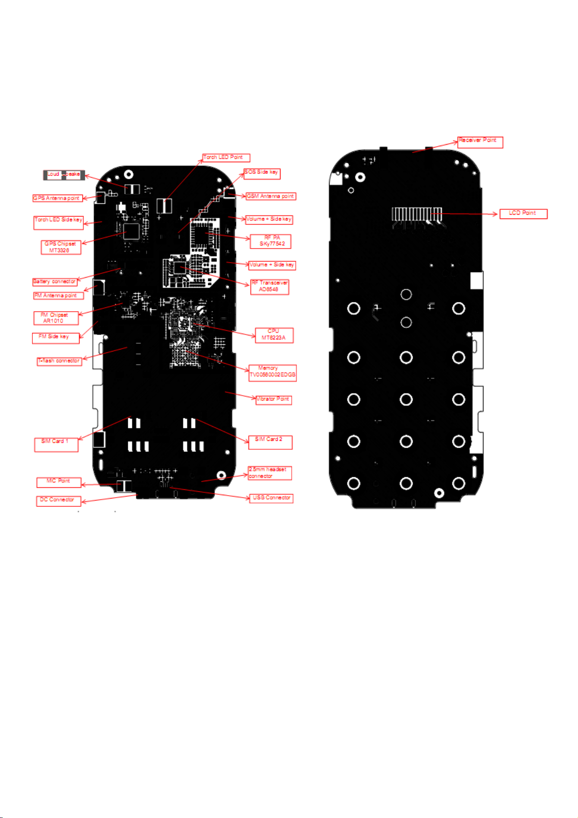
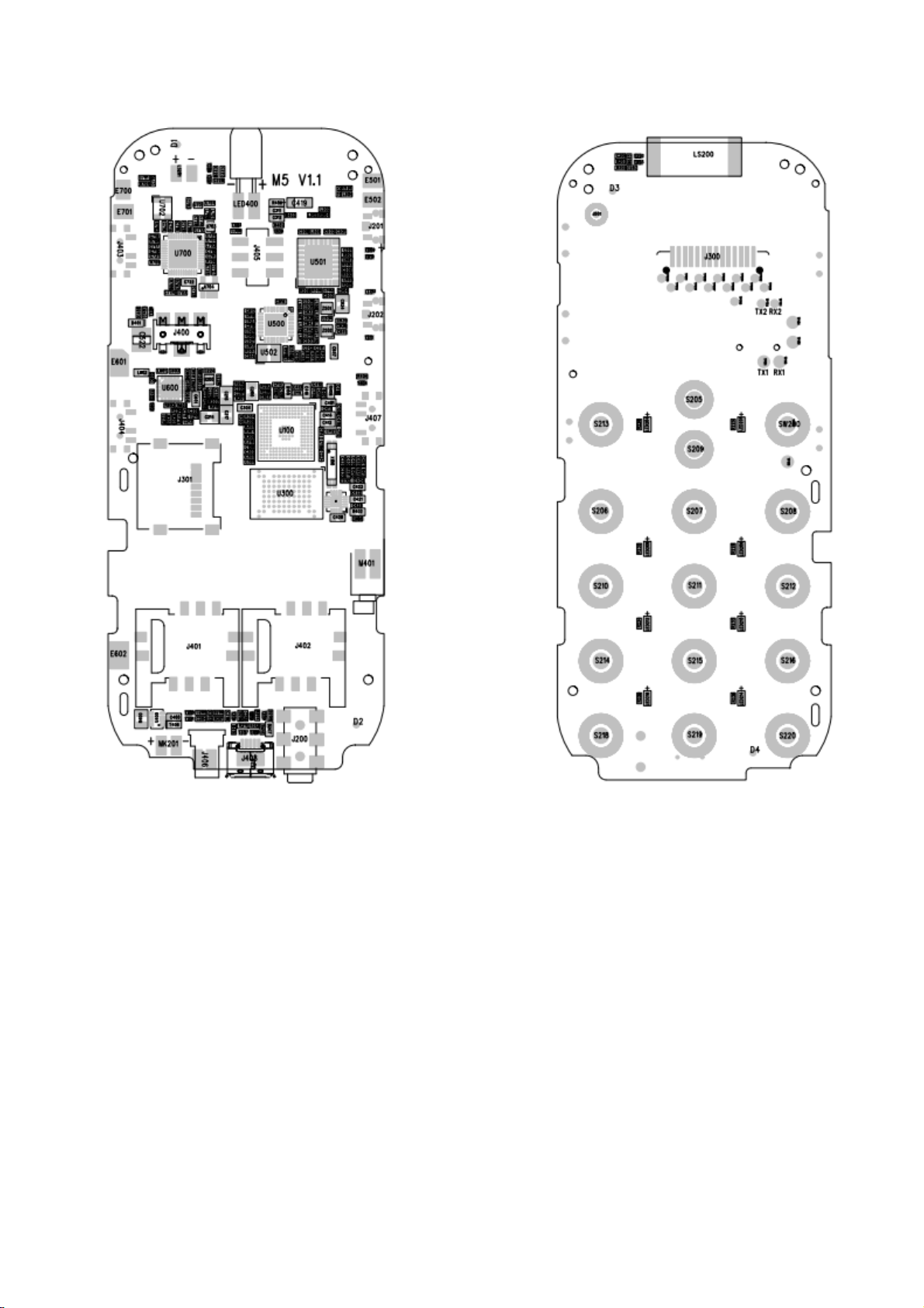
FLY EZZY User manual

.
FLY EZZY
SERVICE MANUAL

CONTEANT LIST
Chapter 1: Summary
Chapter 2: Exploding Diagram
Chapter 3: Explanation of Schematic
Chapter 4: Failure Analysis
Chapter 5: Manual of tool software
Chapter 6: Tools List

ction of practical
ort). It also supports MMS and increment service which facilitate your work and
description of circuit. You can refer to maintaining
Main specification and technique standards of FLY EZZY are as below:
Standbytime:
Styleofnetwork
160-240 hours-
GSM900, DCS180
Chapter 1: Summary
This streamline and comfortable handset is a perfect combination of humanized design and
Excellent craft. Besides the basic call function, FLY EZZY provides you with a colle
Functions including sweet ring tone, cartoon incoming-call animation, File manager
(T-Flash card supp
entertainment.
In order to support technicians to be familiar with FLY EZZY handset, please master the method of servicing.
In addition, we provide corresponding technical data, including CKT base band, RF and software. There are
also many base band and RF test reference points and
examples. Hope it could give you some help.
Talking time: 160-200min

Chapter 2: Exploding Diagram
The main board PCB

The main board placement

Chapter 3: Explanation of Schematic
MTK6223A
AD6548
MTK6223A
Picture 3.1 MT6223A principle picture
3.1 Principle of RF circuit
3.1.1 Principle of receiver circuit
3.1.1.1Rx signal flow chart:
Picture 3.1.1 Receive signal flow frame
3.1.1.2 Main function of RF
RF part generally means the analog RF and IF process system ,including Antenna system、
TX path、RX path、Analog modem and Frequency Synthesizer.

nal
he
Perfo ile phone!
mplifier,
nd the matching components between each other...
ion Receiver
n Baseband Amplifiers
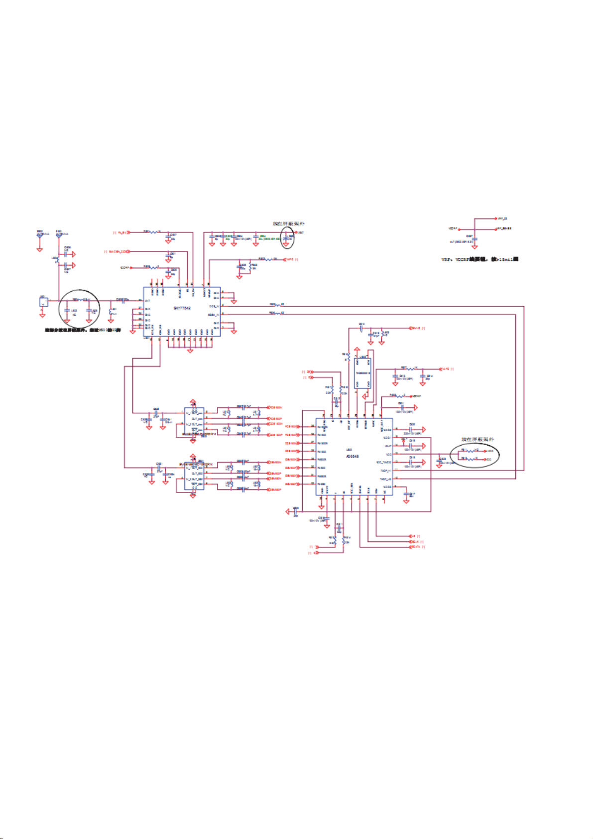
–Th receive path
RF Circuit deals with the RX and TX of wireless signal, with responsibility for the bidirectio
Transmission of speech and data between the MS and BS through the air interface. In detail RX part
Accomplishes the AGC amplifying, mix and demodulation of RF weak signal received from BS, The
Final signal output from RX part is the analog baseband I/Q signal. The final RX I/Q will be sent to
Baseband Circuit for later disposal. On the other hand TX part deals with the signal modulation,
Up-conversion mix and power amplifying of analog I/Q signal received from baseband, generating
Burst which meets the GSM specification. And then the bursts are transmitted to Base station through
The antenna. The signal interface between RF Circuit and Baseband is analog baseband I/Q signal. T
rmance of RF Circuit can directly affects the signal transmission quality of the mob
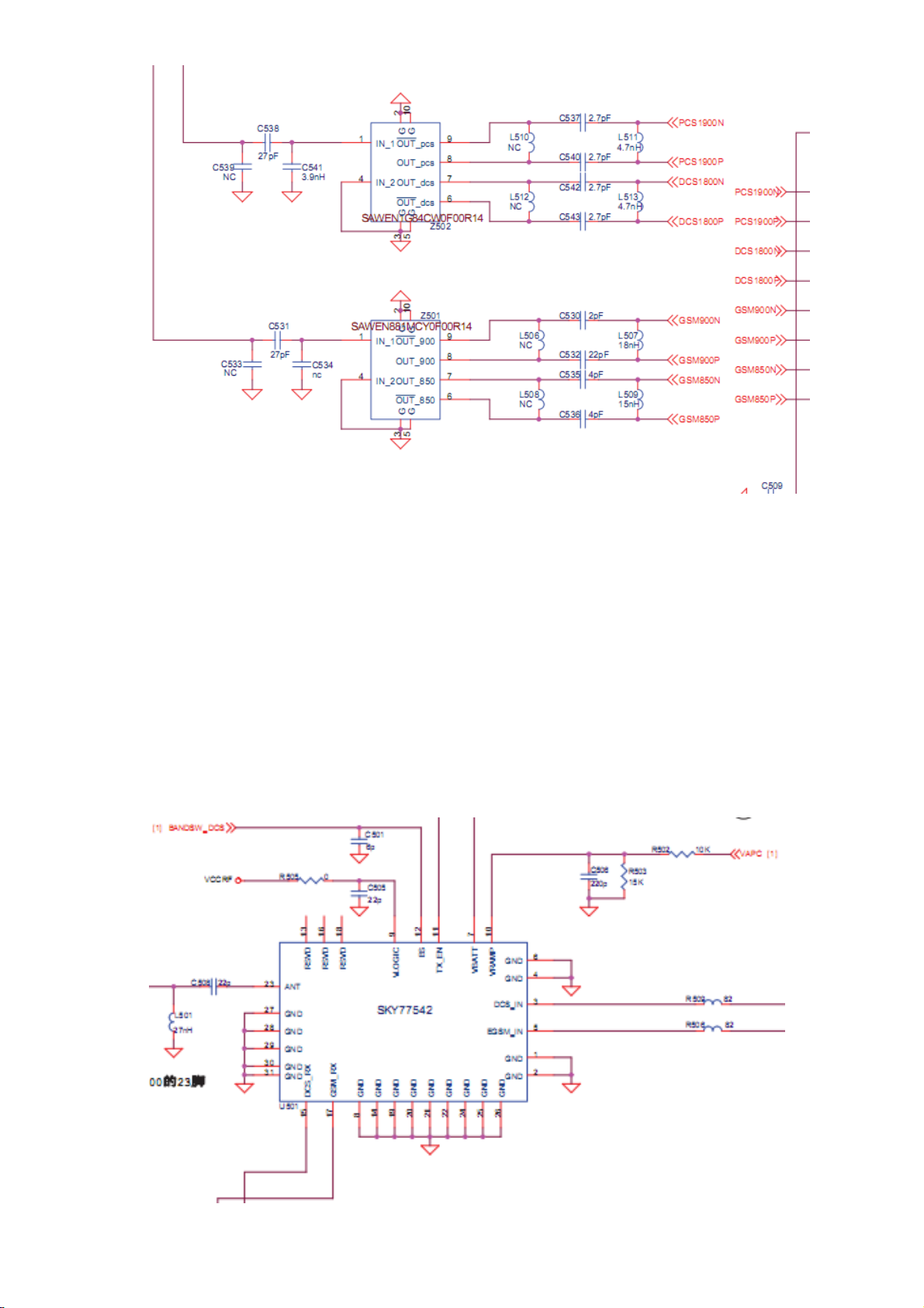
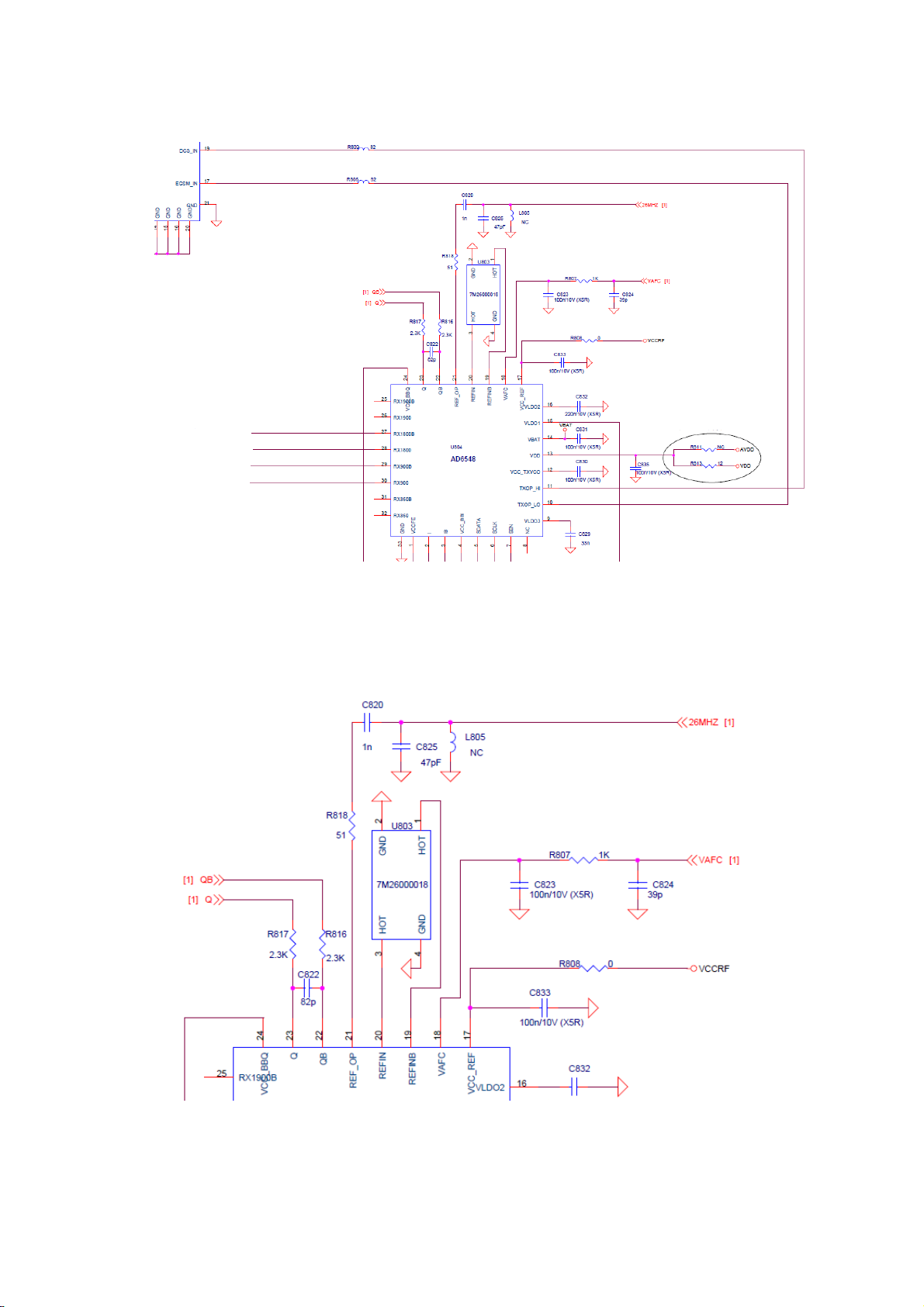
The schematic of RF block for MTK GSM Dual-band RF solution is show below:
From the chart we can see that the RF part is mainly composed of a highly integrated CMOS
Transceiver chip (AD6548), some RX Saw filters, reference crystal oscillator, power a
Antenna switch module, antenna a
3.1.2 Direct Convers
–Differential LNA RX Channel Select Filters–Integrated Active
–Programmable Gai
e

RX Saw filter Circuit
3.1.3 Translation Loop Direct VCO Modulator
–Integrated TX VCO and tank
–External TX filters eliminated
–Integrated Loop filter components
–Transmit Path
AD6548 uses only a single VCO source to derive the local oscillator signal for both the Feedback Down-
Converting Mixer and the Quadraturemodulator
TX PA: SKY77542

CO, tank, fractional N dividers, sigma delta compensation, charge pump and
The only external component is the frequency reference.
26MHz Clock Reference circui
d PLL system
TX PATH:
3.14 26MHz Clock:
–The entire system including V
loop filters are fully integrated.
–
3.1.5 High performance multi ban
–Fast Fractional-N Synthesizer

Integrated Local Oscillator VCO
ters
.1.6 Po
Integrated LDOsallow direct battery supply connection
3.1.7 Frequency ranges
The frequency
TX mode
EGSM900 880.2MHz ~ 914.8MHz
DCS1800 1710.2 MHz ~ 1784.8MHz
–
–Fully Integrated Loop fil
–Crystal Reference Oscillator & Tuning System
3 wer Management
–
The frequency ranges of the synthesizer for RX mode:
RX mode
E-GSM 900 925.2MHz ~ 959.8MHz
DCS 1800 1805.2 MHz ~ 1879.8MHz
ranges of the synthesizer for TX mode

3.1.3 AD6548 Function Block Diagram

3.2Principle of base band circuit
3.2.1 Whole introduction of base band circuit
3.2.2 Explanation of power circuit and in-and-out circuit
Power source is provided by MTK MT6223A and periphery components, main function as below:
A.
B.
C.
2.8V-5.5V Input Range
Charger input up to 8V
Seven LDOs optimized for specific GSM Sub-systems
D.
E. One LDO for RF transceiver
High operation efficiency and Low stand-by current
F. Li-Ion battery charge function
G. SIMCardinterface
H. Two open-drain output switches to control the LED and vibrator
I. ThreeNMOSswitchestocontrolRGBLEDs
J. ThermalOverloadProtection
K. Under Voltage Lock-out Protection
I. OverVoltageProtection
M. Power-onResetandStart-upTimer

1
23A 7 channe supply:
.7 channel power supply
MT62
l power
LDO Power Function
VCORE .5V1.8V/1 Digital core voltage LDO output
VDD 2.8V Digital I/O voltage LDO output
AVDD 2.8V Analog LDO output
VCTXO 2.8V Crystal or VCTCXO LDO output
VMEM tput1.8V/2.8V External memory LDO ou
VSIM .3V1.8V/3 LDO output to SIM card
VRF LDO for RF transceiver
2.8V
2、power on/off circuit

After the handset power off, the pin PWRKEY is pulled high. The pull-up resistance is inside the
chip .When the power key is pressed, the pin PWRKEY is pull low, then the MT6223A turn on all the Power supply
function and the baseband chip enter working status. So the pin BBWAKEUP is pulled high. At that time, the power
key can be released; the CPU-baseband chip can control the MT6223A.
Charge Circuit
MT6223A charge management function:
1、Charger detection
2、Battery voltage measurement
3、Charging current measurement
4、Over voltage Protection
5、Charge mode selection
MT6223A is available to control the pulsed charging current. The pin CHRIN is to detect the
Charger. The pins ISENCE/BATSENES can calculate the battery voltage by detect the voltage of R400, and calculate
the charge current by the voltage of the resistance R400. In different charge mode, Baseband chip sent the
different PWM pulse signal to MT6223A, so the MT6233Acan control the process of charge.
The charge process include three states: pre-charging mode, constant current mode and constant voltage
Mode. If the battery voltage is bellow 3.2V, the handset enter pre-charging mode; If the battery voltage
is over 3.2V, it enter the constant current mode; If the battery voltage is higher than 4.2V, it enter the
constant voltage mode

.
3.2.3 SIM interface
SIM interface circuit
The power management chip supply the interface between the SIM card and baseband chip, the
Key signal is: SIM_CLK (the clock signal), SIM_RST (the reset signal), SIM_I/O (I/O signal),
VSIM (SIM power supply).
3.2.4 Principle of audio frequency circuit
The Audio Frequency (AF) circuit includes three parts: RECEIVER and SPEAKERs, HANDSET
MIC, ERAPHONE and HANDFREE MIC.
There are 4 speakers; each speaker is drove by an AF amplifier. The baseband chip sends the AF
Signal to the AF amplifier though MP3_OUT port. After the AF signal is amplified, it goes to the
Speaker. The RECIEVER is drove by the baseband chip directly. As an electrets tone arm, the MIC
Needs power support when working. The MICBIASP/N port of the baseband chip supports bias
Voltage for Mic. The EARPHONE port of the FLY EZZY is dual-used with the USB port. For more details
Please refer to “communication ports” in later part.

1、Receiver
Figure 3.2.5 Circuit of receiver
2、Louder speaker
Figure 3.2.6 Circuit of louder speaker

3、
igure 3.2.7 Circuit of MIC bias voltage circuit of mobile phone
、Hands-free microphone
Figure 3.2.8 Circuit of Hands-free microphone
Handset microphone Earphone
F
4
3.2.5 LCD circuit

Memo generation base band chip
That made the system structure to separate
The periphery equipm nd all of them use the 52M
System clock simu
LPA0 is select
set signal.
Display data is transferred to video RAM in LCD driver by I/O port in DMA mode. So system
Can response quickly and multimedia runs fluently without mosaic or picture feeling. Three
Common-anode LEDs in charge of background light supplying. Three voltage sensitive resisters are
Needed to protect the LCD from electrostatic harm and extend the life of LCD.
ry and all the periphery equipments used the same bus based on the 1st
very slow. Considering that, MTK have altered the hardware
ents (like LCD and NAND etc.) from memory bus a
ltaneously
Figure 3.2.9 LCD interface circuit
LCD use series type LCD and four control bus (LPCEOB_MAIN_LCM is chip select signal;
bus for register and commend; LWRB is LCD writes strobe; LRDB is LCD read strobe, LRSTB is re
LCD is controlled by baseband IC.

3.2.8 T-Flash circuit
T-Flash card interface: VDD is supplied by MT6233A
3.2.10 FM
U600 is the FM chip to supply the function of FM radio.

3.2.11 key interface
s,
Then Baseband can judge the key’s location, so system implements corresponding function.
When key is pressed down, the matrix KCOLX status is pulled down to low. Interrupt occur
Table of contents
Other FLY Cell Phone manuals