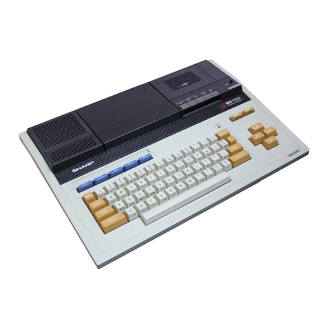
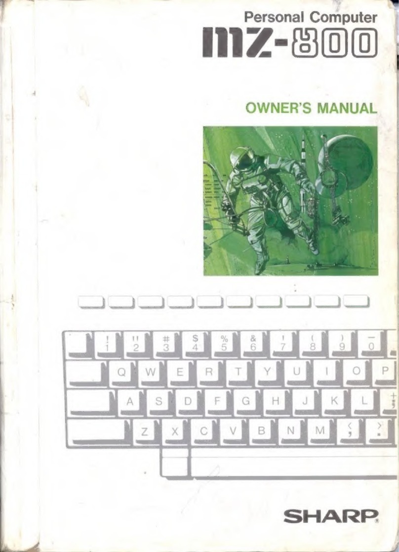
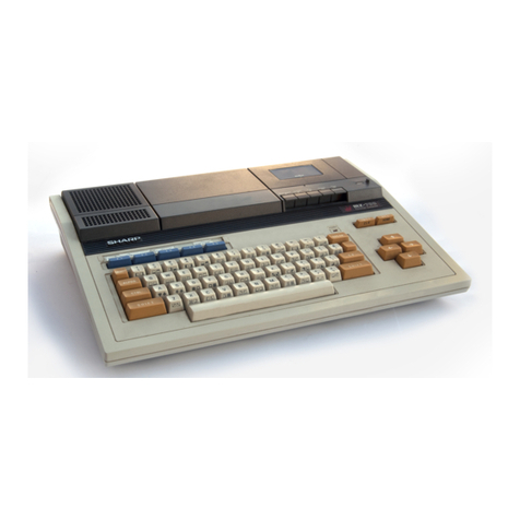
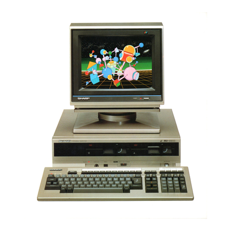
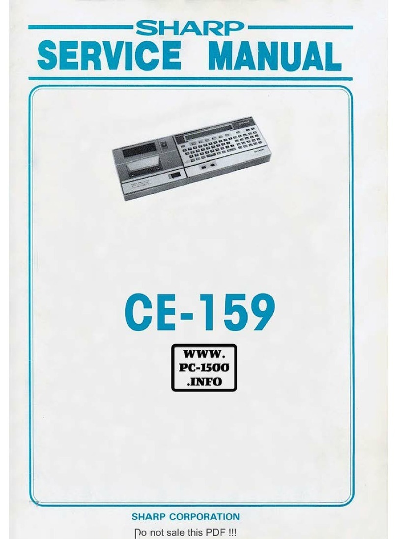
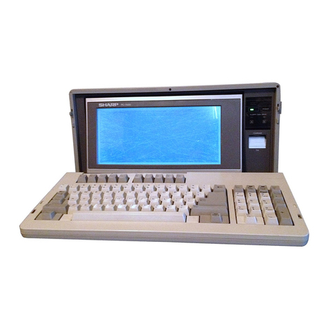
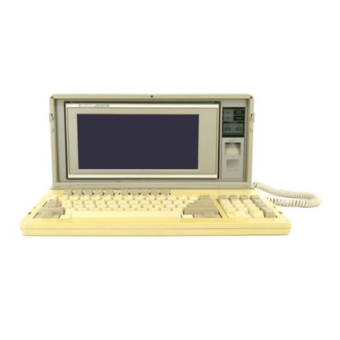
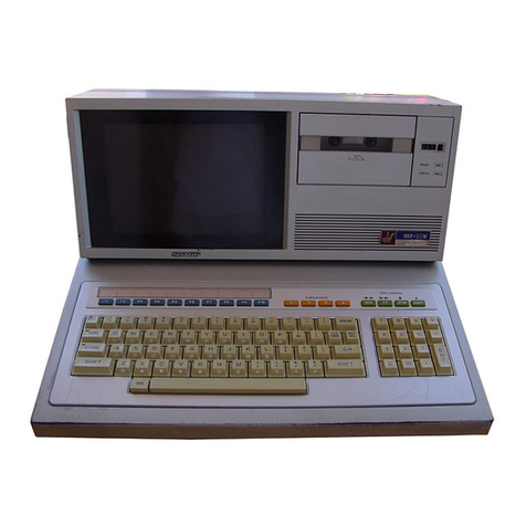
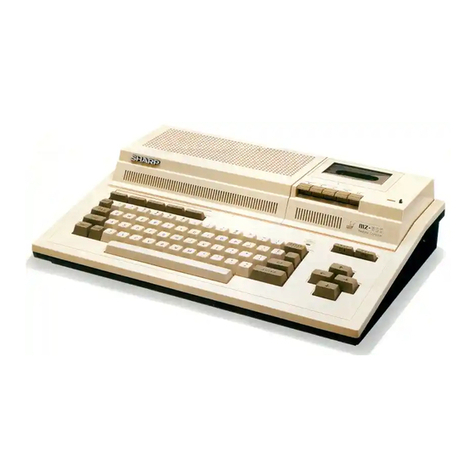
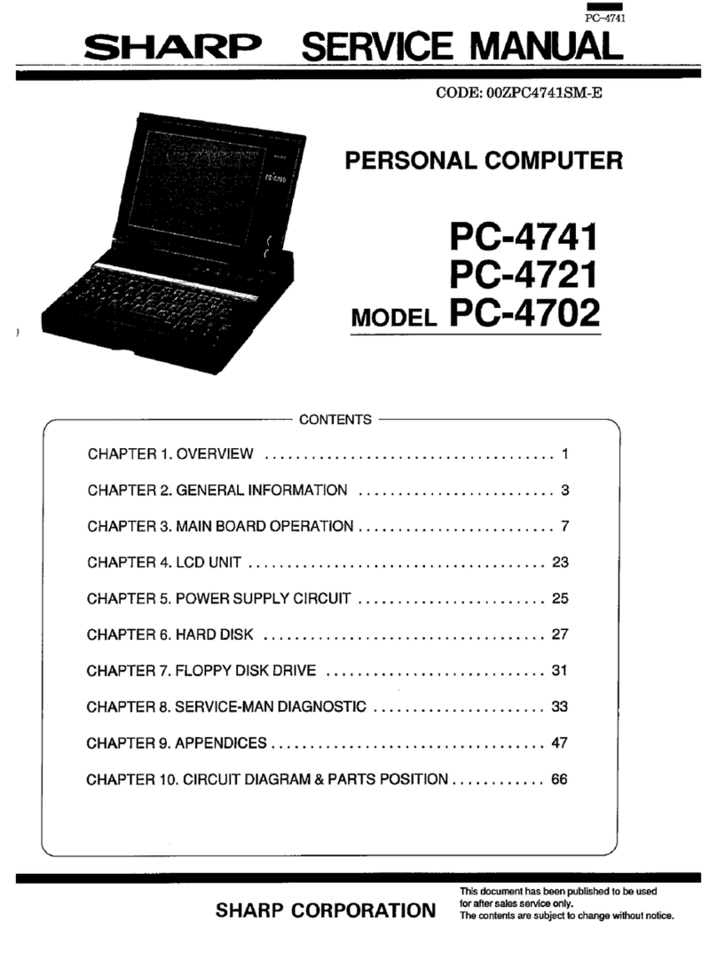
Sharp MZ-800 Use and care manual

Personal Computer
lllZ·OOrnJrnJ
TECHNICAL REFERENCE
MANUAL
SHARR,

Personal Computer
111Z·00(Q)(Q)
TECHNICAL
REFERENCE
MANUAL
©SHARP
CORPORATION

CONTENTS
MZ-800
HARDWARE
1
System
description ······························ ························································· 1
2 Block
diagram
2
3
Memory
map
······
···············
·········
································································
·· 3
4
Custom
LSI
·•
···············································
·······
··········································· 6
4-1
Memory controller ····························································································· 6
4-2 1/0 controller ··································································································· 6
4-3 Clock generator
and
timing generator ···········.......................................···········
··
9
4-4 Display address generator ················································································· 9
4-5 Scroll ············
··
·············
··
··
··
········
··
···
··
············
··
·············
··
·····
··
·····
··
·······
··
······
··
···
10
4-6 VRAM data input/output circuit ·························
··
············································· 12
4-7 Register functions ···········································································-················· 17
4-8 Pallet ····································································································-···-·-· 22
4-9
CRTC
register map ··································-······················································· 23
4-10
ROM
configuration ··························································································
24
5
8255
Programmable
Peripheral Interface
.........................................................
24
6
8253
Programmable
Interval
Timer
·······················
·····
····················
..................
28
7
Printer
interface
··································································
···························
28
8
Programmable
sound generator
·····································································
31
9
Joystick
····
····················
·····
··
······
··
······
·····
····································
······
·········· 32
1
0
Power
supply ····························································································· 33
10-1 Block diagram ································································································ 33
10-2 Operational description ············-·····························-·········································
34
10-3 Maintenance ··································································································· 34
10-4 Problem determination
and
sequence
··································································
34
11
MZ-1P16
···································································································
35
11-1 Installation ······································································································ 35
11-2 Block· diagram ................................................................................................ 36
11-3 At power
on
··································································································· 36
11-4 Colour change operation ···················································································· 36
11-5
Pen
change operation ······················································································· 36
11-6
Pen
exchange method ······················································································· 37
11-7 Stepping motor driving signal ··········································································· 37
11-8 Colour position detector ···················································································· 37
11-9 Character set ···································································································
37
11-10 Colour plotter printer control
LSI
········································································
38
11-11 Interfacing with the MZ-800 ·············································································· 39
11-12 Block diagram ................................................................................................ 39
11-13 Colour plotter printer control
codes
·····································································
40
11-14 Graphic mode commands ·················································································
41
11-15 Specification ··································································································· 42
11-16 Circuit ············································································································ 42
12
CPU P.W.B. Circuit
·······················································································
43
ii

MZ-800
SOFTWARE
1 Character
generator
(C.G.)
··············································································
45
1·1
How
to modify
e.G.
ROM
················································································· 45
1-2
e.G.
Table ··············································'······················································· .46
1·3
e.G.
ROM
dump list ··························································································
48
2 MZ-800
Monitor
subroutines
...........................................................................
52
3 Assemble
list
....
~
...........................................................................................
67
3-1
Monitor<
1Z-0138>
....................................................................................... 67
3-2
MZ
Disk control < 9Z-504M-Vl.Oe> ..................................................................100
3-3 Mini-floppy disk control ...................................................:................................111
3-4
ROM
Monitor ............................................................................................,........117
4 Z-80
Programming
reference
...........................................................................
138
4·1
Z-80
Status indicators (Flags) ............................................,..............................138
4-2 Notation .........................................................................
~
.....····························140
4-3
Z-80
Instruction
set
.............................;............................................................141
INDEX
···············································································································173

1 System description
~-ceu
I I
Z~A
I
IL..-
____
.....J
Basic
RAM,
64KB
PPI
8255
0 =
3.547
MHz
_j~
~~--------~~~-C-M_T_V_F--~1~_.------4-~
I
L:
CTC
8253
MONITOR
CGROM
L.-------.....J
16
KB
r---,
I I MZ-1P16
OP
I r
-.L-
-
--,
1
l_~
Plot printer 1 J
l_
/
--J
~-
PlO
Z-80
PlO
L__j
I ·
MZ80P5K
printer
~
Printer interface
Jl)-'-
.,...,...-
-----
1
-,_
,-----t---lL:Jo:y~st:ic=k~in~t:erf:a:c:Je~~
PSG
SN76489
.~
L..-.-------1
r_{_""l l
Expansion slot-1
~
(ATARI
compatible
.l
RGBI
CRTC
'(
VRAM
16
KB
(Semi-custom)
r
..,
I VRAM I
r--
.&...
RF
Color 1 I
encoder I
.--0
~
Video
HZ-1R25
16
colors
CRT
)
MZ-1019
l
0
0 0
TV
I I
MZ-1R18
slot I
\I,,,
..
..,,
I
L--
_._.J
__
I
16
KB
(OP)
I
___
L
______
....J
___
__j
MFD
MZ-1F02
1
RS·232C
MZ-88103

!17.73
MHz
0 = 3.547
MHz
CPU
~
"
,_
E
_l
~
Option 16
KB
RESET
GDG
VRAM ADR. BUS VRAM
16
KB
VRAM DATA BUS
~
~
I
~,,.
••
IC
:;'
VRA5
WE
CAS
ADDRESS BUS
J DATA BUS
ICJ
~11
CONTROL BUS
L_
r-
.._
Peripheral
VO
bus
r===Jn
I 1
•,1
C~~T
Ogj
L...-.r
8253 h
n
.,
"'
.0
J J
..i.l~
c:
.~
.,
c:
.,
c.
X
w
v
~
Z-80A
L--------:---11-><
OSCI Cursor
556
KEY
DATA
PA
8255 I PlO
OUT2~------;PA5
.!1
.,
>-
0
PBI
PRINTER
DATA
BLJS~
\0
CTRL
BUS
~
-,
~/"""'
PC21
I I I
t---
I~
~
~"
~
~·
KEY
STROBE
r
:BOAR~
J w
AMP
DATA
RECORDER
PA'
~f)II.__L___.____:.
l~~
~~
System switch
.)J (MZ -Centronics)
VBLN--fPA4
SP
External
printer
bus
I\)
D:l
0
0
';11:"
c.
~·
CO
...
I))
3

3 Memory map
The MZ-800 has a different
memory
map depending on
Q MZ-800
memory
map
EOOO
0000
MAIN
D-RAM
8000
-----
-64-K&-- -
4000
2000
1000
oooo.
MZ-700mode
D
bd
.---,
~
~
ROM
VRAM
MZ-800
mode
MAIN
D-RAM
the mode. To have compatibility
with
the MZ-700, it has
two
modes
of
the MZ-700 mode and MZ-800 mode.
~
t:J
-
[]
\J
D
DV-RA~--,
I I I I
I I I 1
I I l D I
!m}
I
I : : :
------
-L
••
.J
._
__
J
r---,
I I
I I
:
IIVI
I
' I
o I
L--..1
~
640 x 200
mode
~
VRAM
320 x 200
mode
NOTE:
r---.
I I
:m:
I I
...
__
.J
Item
within
darted line
represent!l an
option
unit
MZ-1R2S
Memory
map
changes after initial program loading
$0000
$1000
$2000
@ Power
on
(reset)
MZ-800
mode
MON. ROM
CG.
ROM
DRAM
@At
start
of
monitor
MZ-700
mode
$0000
...--------.
MON.
ROM
$1000
~------1
LD
A,
OSH
©Write
to
PCG
from
CG
MZ-700
mode
$0000
$1000
$2000
MON.
ROM
CG.
ROM
@ System operation
MZ-700 & 800
modes
$0000
OUT
(CE), A IN
(EOH),
A
$8000
=>
DRAM
V-RAM
(320x200
mode)
DRAM
$0000
V-RAM
$EOOO $EOOO
$E010
MON.
ROM
MON.
ROM
$FFFF
$FFFF
• Memory map at
power
on
is
in
the MZ-800 mode
as
in
@,
but
it changes
to
the MZ-700 mode by the
monitor
ROM
when the
monitor
program starts. After
transferring the
CG
data
to
the VRAM
PCG
area
from
the
CG
ROM
at @, the
memory
map then returns
to
@.
• When the system program is completed
to
load, the
memory
map goes into the MZ-700 mode
if
the
system switch (SW1) is set
to
ON
side. If set
to
OFF
side, it changes
to
the MZ-800 mode, then the
memory
map
as
in
@.
During those changes, all
memory
spaces are composed
of
RAM and isolated
from
ROM
and VRAM.
3
D-RAM
D-RAM
==>
IN (E1H), A
<=
$COOO
V-RAM (CG)
$0000
V-RAM
$EOOO
$E010
MON.
ROM
$FFFF
SFFFF
'---------'
• Depression
of
the manual reset switch
~ssumes
memory
map transition in order
of
@
---+
@
---+
@
---+
@, similar
as
in the case
of
power
on.
• ·However, depression
of
the reset switch in conjunc-
tion
with
the I
CTRL
Ikey assumes the
memory
map
of
@after
being changed once
to
the MZ-700
or
MZ-800
mode depending on the state
of
the system switch. In
the case
of
the MZ-800 mode,
it
is set
to
the plane I,
II
(4-color mode)
of
the 320 x 200 mode.

~t
rt
$EO
MODE -
Function o $0000 -
$7FFF
to
DRAM.
0000 T
1000
2000
3000
4000
DRAM
5000
6000
7000
8000
9000
AOOO
8000
cooo
DODO
I
EOOO
I
E070
I
FOOO
I
I
FFFF
L
__
_j
Memory Bank Control
$E1
$E2 $E3
$E4
MZ-700
mode
MZ-800
mode
-MZ-700
mode
MZ-800
mode
MZ-700
mode
MZ-800 mode
o $0000 -
$FFFF
o
$EOOO
-
$FFFF
o $0000 -
$0FFF
o $0000 -
$FFFF
o
$EOOO
-
$FFFF
o
$0000-
$0FFF
o $0000 -
$0FFF
to
DRAM.
to
DRAM.
to
monitor
to
VRAM, key
to
monitor
to
monitor
to
monitor
ROM. timer, and ROM. ROM. ROM.
monitor
ROM. o
$1000-
$CFFF
o
$1000-
$1FFF
to
DRAM
to
CG
ROM.
o $0000 -
$FFFF
o $2000 -
$7FFF
to
VRAM, key and
timer, and
$COOO
-
$DFFF
monitor
ROM.
to
DRAM.
o $8000 -
$BFFF
to
VRAM
(NOTE).
o
$EOOO
-
$FFFF
to
monitor
ROM.
~--l
,---,
,--,
~--,
I MONITOR
I I I ROM I I I I
I
I I I I I I I
I
I I I I I I
I I I I I
I I
I I I I
I I I I I
I
I I
I I I I
I I I I I I
I I I
I I
I I I I I
I I I I
I I I
I I
MONITOR
ROM
DRAM
MONITOR
ROM
CG
ROM
DRAM
I I
I I
I
I
VRAM
I I I
----
I I I
I I
I
I I I
I
I I
I r I
I I
VRAM
I
VRAM
(NOTE)
DRAM
B
KEY,
TIMER
DRAM
I
I I MONITOR MONITOR
I ROM ROM
I
L
__
j
KEY,
TIMER
MONITOR
ROM
MONITOR
ROM
Area
within
dotted line does
not
involve
change.
____1
(NOTE): In the case
of
320 x 200 mode, contents
of
$8000-
$9FFF
are transferred, instead,
and those after
$AOOO
are transferred
to
DRAM. Power on
or
RESET
input
4

~
OUT ($E5) OUT ($E6) IN
($EO)
IN ($E1)
MODE MZ-700
mode
MZ-800
mode
MZ-700
mode
MZ-800
mode
MZ-700
mode
MZ-800
mode
MZ-700
mode
MZ-800
mode
Function o
$0000
-$7FFF o
$EOOO
-
$FFFF
o $0000 -
$FFFF
o
$EOOO
-
$FFFF
o
$1000-
$1FFF o
$1000-
$1
FFF
o
$1000-
$1FFF o
$1000-
$1FFF
prohibited. prohibited.
returned
to
retur'led
to to
CG
ROM.
to
CG
ROM. returned
to
returned
to
the
state be-
the
state be- o
$COOO
-
$CFFF
o $8000 -$BFFF
the
state
be-
the
state be-
fore
prohi-
fore
prohi-
toVRAM
(PCG
to
VRAM
fore
CG
was
fore
CG
was
bited. bited. RAM). (NOTE). set. set.
o
$COOO
-
$CFFF
o $8000 -
$BFFF
to
DRAM.
to
DRAM.
0000
,--l
~--l
,--,
,--,
~--l
,--, ,--,
r--~
I I I I I I I I I I I
1000 I I R
~
B B
I
2000 I I MM
I I I I I I I I
I I I I I I I I
3000 I
I I I I I I I I
4000 I I I I I I I I
I I I I I I I I
5000 I I I I
I I I
I I I I I
8000 I
I I I I I I
7000
I·
I I I I I
I
I I I I
8000 I
I I
9000
VRAM
I I
I
AOOO
r----
I I
DRAM
I
BOOO
(NOTE)
~
cooo
VRAM
I
(CGRAM) I I
0000 I I I
EOOO
I I I I
Prohibited State before I I I I
prohibited
I I
FOOO
Prohibited
State before I I I I
prohibited
I I I
I I I I L
__
j
FFFF
L
__
_j
L
__
_j
L
__
_j
5

HARDWARE

4 Custom
LSI
The custom
LSI
is a 100-pin single chip
LSI
on which the
MZ-800
memory
controller
(110
controller) and
CRT
controller, etc. are contained.
4-1
Memory controller
Used
for
the control
of
the
memory
bank. Addressing
of
DRAM, ROM, and VRAM is conducted by selection
110
address,
$EO
-
$E6,
using OUT
or
IN
command.
1/0
Signal Device
(1/0)
address name ,
4-2 1/0 controller
In
this
1/0
controller is created the select signal
for
assignment
of
MZ-800 internal device.
See
Table-2
for
relation
of
internal device vs
110
address.
Function
FF
Port
B,
printer data output
FE
CPR
Z80A Port A, printer control and timer interrupt
FD
PlO
(110)
Port B control (Mode
0)
FC
Port A control (Mode
3)
F2
PSG
PSG
(0)
PSG
output
port
F1
JOY JOYSTICK
(I)
Joystick-2
input
port
FO
Joystick-1
input
port
FO
--
(0) Pallet
write
E6
l
--
--
(110)
Memory
bank control
EO
07
Control
port
output
06
C53
8253
(110)
Counter-2 (NOTE): Mapped
to
E007
-
E004
in the
os
Counter-1 MZ-700 mode.
04
Counter-0
DJ Control
02
KEY
8255
(110)
Port
C,
cassette, etc. (NOTE): Mapped
to
E003 -
EOOO
in the
01 Port 8, key
input
MZ-700 mode.
DO
Port A, key strobe output
CF
0
CE
110
CRTC
register
CD
--
--
0
cc 0
$E008
--
--
110
TEMP, HBLK input; and 8253
GO
ON/OFF
output
for
the MZ-700 mode only.
.,
When above 1/0 address is accessed,
it
makes IOWR active
for
OUT
or
lORD
for
IN
command.
6

Pin Signal
name
1/0
Functional
description
Note
No.
1
CPU
0
CPU
clock (3.547 MHz)
2
5V
-
Power
supply
3 GND -,Ground
4
ADO
I I I
CPU
address bus
19 ADF
20
DTO
I I
1/0
CPU
data bus
27
on
28 GND -
Ground
29
vcc
-
Power
supply
'
30
MREO
I
CPU
MREO
signal Negative logic
31
RD
I
CPU
RD
signal Negative logic
32
WR
I
CPU
WR
signal Negative logic
33
RFSH
I
CPU
RFSH
signal Negative logic
34
IORO
I
CPU
lOAQsignal
Negative
logic
35
M1
I CPU
M1
signal Negative logic
36
SEL1
0 System RAM address
multiplexer
select signal
37
CASB 0 System RAM
column
address
strobe
signal
38 INH5 0
Inhibit
bank (OUT $E5) select signal
("H"
-Inhibit).
OPEN
39
VBLN
0 Vertical blanking signal Negative logic
40 GND -
41
VRAS
0 VRAM RAS
control
signal Negative logic
42
VCAS
0 VRAM CAS
control
signal Negative logic
43 VADO
I I 0 VRAM address signal
(multiplexer
output)
50 VAD7
51
WE
0 VRAM
output
enable Negative logic
52
vcc
-
Power
supply
53 GND -
Ground
54
VRWR
0 VRAM
write
signal Negative logic
55
VAO
I I
1/0
VRAM data bus (standard RAM)
62
VA7
63
vco
I I
1/0
VRAM data bus
(option
RAM)
70
VC7
71
SBCR 0 Calor sub-carrier
wave
72
RED
0 Video signal, red
73 BLUE 0 Video signal, blue
74 GREN 0 Video signal, green
75 V
ITN 0 Brightness
control
signal
76
VSYN
0 Vertical sync signal Negative logic
77
HSYN
0 Horizontal sync signal Negative logic
78 GND -
79
vcc
-
80
CLKO
I Clock
input
(17.7344 MHz)
81
CROM
0 ROM
chip
enable Negative logic
82
KEY
0 8255
chip
enable Negative logic
83 NTPL I NTSC/PAL selection (PAL -
"L")
GND
84
TEST I Test
pin
("H"
-test
mode)
GND
85 MOD7 I MZ-700/800
mode
selection
("L"
= MZ-700
model
86
IOWA
0
Sum
of
CS
and WR
of
1/0
controlled
by
the
custom
IC
Negative logic
87
lORD
0
Sum
of
CS
and
RD
of
1/0
controlled
by
the
custom
IC
Negative
logic
88
CRS
0
1/0
$BO
-$B3
chip
enable OPEN
89 SIO 0
1/0
$F4-
$F7
chip
enable OPEN
90 RSro 0 Reset
output
Negative logic
91
MNRT
I Manual reset
input
Negative
logic
92
PORT
I Power
on
reset
input
Negative
logic
93 WTGD 0
Wait
signal
to
CPU
Open drain
94
""JOY
0
Joystick
chip
enable Negative
logic
95
CPR
0 PlO
chip
select Negative logic
96
PSG
0 76489 chip select Negative
logic
97 CKMS 0 8253 musical interval clock
98 53G 0 8253 musical interval ON/OFF gate signal
99 C53 0 8253 chip enable Negative logic
100 TEMP I MZ-700
mode,
$E800
tempo
input
*Term
"OPEN"
represents
the
signal
not
used
on
the
board.
7

Pin configuration
CPU
AOO
•o•
AOJ
AO<
A01
A08
AOO
AOS
AOO
AOE
AOF
on
OT2
OT<
OTS
OTO
OT7
GNO
TEMP
!'.JG
PSG JOY PORT RSTO CPS
IOWR
TEST KE'f
C53
CKMS
CPR
WTGD MNRT
SIO
lORD MOD7
NTPL
CROM
1m
"'R'FSil
Rf
'(7;H
WIJi
Vlti:S"
VAOO
VAD2 VAD4 VA06
WJf
~
SELt !NHS GND
vt:A3"
VA01
VA03
VAD5 VA07
CLKO
v.
GREN
BLUE
REO
SBCR
VC7
vco
VCJ
VCO
VAl
VAA
VAO
GNO
Custom
LSI
block diagram
VSYN
SBCR
HSYN
VBLN CKMS
CPU
CLKO
NTPL
ADO-
F
DTO
-7
RD
WR
MREQ
M1
IORQ
RFSH
CROM
SEL1
CASB
I
NHS
CPR
KEY
C53
53G
JOY
PSG
CRS
SIO
lORD
IOWR
WTGD
16
8
I
Clock generator &
timing generator
CPU
address
CPU
CPU
VF
CONTROL
f..--
Memory
I--
controller
----
1/0
controller
WAIT
controller
+
r-l
Display address
generator
,.------
!
DATA I
'I~
f---------1
MPX I
Hisplaycontrol
.--
register t
I--
~Scroll
register~
r----
Scroll circuit
! t
MPX I
VRAM address
controller
!
I MPX
JVRAM I
-~
Timing control 1
1 8
VRAS
VCAS
VRWR
VAD0-7
VROE
8
I
V
cc
2,
29,
52,
79,
pin
GND 3, 28, 40, 53, 78 pin
PORT
MNRT
RESET
,...-----
Input
BUFF
'-----
Pallet
circuit
Shift
register
+
VRAM data
VO
circuit
ts
8
VA0-7
VC0-7
RSTO
MOD7
TEMP
RED
GREN
BLUE
YITN

4-3 Clock generator and timing generator
Oscillation
from
the crystal oscillator is divided
to
create
the
CPU
clock, horizontal sync, vertical sync, and dis-
play address control signals.
Since the
low
state
of
signal is used
for
NTPL (NTSC/
PAL selection)
with
the MZ-800, the
CPU
clock
of
3.547 MHz is derived
from
the crystal frequency
of
17.734 MHz
by
dividing
it
1/5.
Clock generator and
timing
generator circuits
Display address generator block diagram
9
4-4
Display address generator
1)
Display address generation
• Display address increments
from
left
to
right
as
beginning
from
the home position at the upper left
corner
of
the
CAT
screen (address $000). The first
display line dominates address $000 through $027.
Because a screen frame consists
of
200
rasters, the
address at the right side
of
the
bottom
corner is
as
follows:
(200
X 40) - 1 = 7999 =
$1
F3F
• The address counter stops counting
for
a horizontal
flyback line and stored in the address latch circuit.
When the horizontal flyback line terminates, the
address latch
output
is preset in the address counter
(display address generator).
• Address is generated even
while
the vertical flyback
line is active and
it
makes the counter reset before
termination
of
the vertical flyback line.
2)
Display address generation in the MZ-700 mode
• Because characters are displayed under the
PCG
method in the MZ-700 mode, address is generated
for
each character and the same address is used
for
displaying
of
one character. The 3-bit horizontal line
counter is provided
to
count horizontal lines
to
generate the address
(LCO
-
LC2)
for
selection
of
the
character front.
Display address increments
from
left
to
i-ight having
the uppermost left corner
of
the screen
for
the
home
position.
Since
25
lines are used
to
develop displaying
of
characters composed
of
8 x 8 dots, the address at
the right
of
the bottom lines becomes
$3EF.
3)
Display address multiplexed
with
CPU
address
• Address used
to
write data
to
the VRAM is latched in
order
to
avoid
CPU
wait. Display modes
of
640 dots
and 320 dots are assigned by the mode switch
(DMD2).
• Display address is multiplexed
with
the VRAM write
address in the
timing
of
DISP
which has the timing
that the display address and
CPU
address may
become a pseudo cycle steal.

4-5 Scroll
1)
Scrolling is possible
for
both horizontal and vertical
directions by means
of
software offset.
The
following
four
registers are used for scroll
control.
a.
Scroll start address register: SSA (7-bit)
b.
Scroll end address register:
SEA
(7-bit)
c.
Scroll
width
register: SW = SEA-SSA (7-bit)
d. Scroll offset register:
SOF
(10-bit)
I
SSA~
; :
-~--;.'-
-3
--
------
--
s~l__.
~!
_____________
_
2)
Control
of
scroll starts by the initialization
of
the
scroll control register.
SSA = $0
SEA=
$7D
SW = $7D
SOF
= $0
3)
Way
of
smooth scrolling
SOF
= $0-.... $5
Programming "SOF = $5" makes the display screen
shifted one line up.
The highest line (address:
$0
-$27) is then assigned
to
the lowest line
($1
F18
....:
$1
F3F).
As normal scroll involves updating
of
the data
for
the
lowest line, the data
of
address
$1
F18
-
$1
F3F
are
updated.
SOF
= $5-.... $0
By reducing the value
of
SOF
by
"5",
it
makes the
screen shifted one line down.
SSAr---------------------------~
SEAL---------------------------~
4)
line
scroll
SOF
= $0-.... $28
Programming "SOF = $28" makes the display screen
shifted eight lines up. Data on the highest line
therefore shifted
to
the bottom line.
Programming "$28
-....
$0" makes the display screen
shifted eight lines down, and the line on the bottom
moves to the highest line.
5)
Screen split
10
Appropriate deviation
of
SSA, SEA, and SW permits
to divide the screen into three sections
of
@,
@ and
©-
Though the section @ is permitted
to
scroll, sections
@ and © are
not
permitted
to
scroll.
See the figure
to
explain with.
SSA--.
@
SEA---
----
©
Assume
now
that the
top
of
the section @ is on the
5th line
(40
raster) and the
top
of
the section © is on
the 18th line (144 raster). Attention must
be
paid
to
the fact that values SSA .and SEA are used
for
assigning lines. Scroll registers are set
with
the
following values.
SSA = $19
SEA=
$5A
SW =
$41
SOF
=
$0
•
In this occasion,
it
needs
to
initialize the screen that
has been displayed. "SOF = $5" must be program·
med
to
scroll @ one line. Then, only the section @
is
shifted up, and the highest line
of
@ moves
to
the
bottom
line
of@.
Programming "SOF =
$A"
makes
i1
scrolled one
more
line.
SOF
~SW
Scroll offset (SOF) should necessarily .be
within
c
range
of
the scroll
width.
Display is
not
assured
wit~
SOF
set greater than SW.

Scroll and control
circuit
hardware
• Block diagram
DA(MA)
7
Relation
of
display address, SEA, SSA, vs
SOF
Display
address
m I k j
SSA SSA
SSA SSA
SSA
6 5 4 3
SEA SEA
SEA
SEA SEA
6 5 4 3
SOF SOF
SOF
SOF
SOF
9 8 7 6
Screen
left
end
address
0
Line
0 0 0 0
1
Line
0 0 0 0
2
Line
0 0 0 0
3
Line
0 0 0 0
8
Line
0 0 0 0
16
Line
0 0 0
24line
0 0 0
192
Line
199
Line
Relation
of
SW vs SOF
SW>
SOF
i h
SSA SSA
2 1
SEA
SEA
2 1
SOF SOF
5 4
0 0
0 0
0 0
0 0
1 0
0 1
1 1
0 0
0
11
Scroll control register
SSA: Scroll start address
Increment
of
SSA:
$5
Minimum
value
of
SSA:
$0
Maximum
value
of
SSA:' $78
MSB
LSB
N 6 5 4 3 2
SEA: Scroll end address
Increment
of
SEA: $5
Minimum
value
of
SEA:
$5
Maximum
value
of
SEA: $70
MSB
LSB
N 6 5 4 3 2
SW: Scroll
width
Increment
of
SW: $5
Minimum
value
of
SW: $5
Maximum
value
of
SW:
$70
Relation
of
SW, SEA, vs SSA
SW=
SEA-
SSA
SW>
SSA
MSB
LSB
N 6 5 4 3 2
s~
I
SOF:
Scroll offset
Increment
of
SOF:
$5
Minimum
value
of
SOF:
$0
(without
offset)
Maximum
value
of
SOF:
$3E8
MSB
LSB
SOF
1 I 7 6 5 4 3 2
S~F
I
MSB LSB
SOF
2~------------~
9
S~F
I
g I f e d I c b a
SSA
_ -
0
SEA
I
S~F
fs~F
S~F
~-
SOF
3 2
I I
I
0 0 0 0 0 0 0
0 1 0 1 0 Q 0
First
line
1 0 0 0 0 0
1 0 0 0
1 0 0 0 0 0 0
Second
line
0 0 0 0 0 0 0
Second
line
1 0 0 0 0 0 0
0 0 0 0 0 0 0 Twenty fifth line
0 0 0 0 0

Concept of
the
.scroll
control
C!ircuit
Scroll
method
• Scrolling
by
means
of
VRAM address conversion.
Range of scroll
• y-axis programmable.
BASIC
console command compatible
• x-axis fixed
Scroll
sequence
• The scroll start address is termed
"SSA"
and end
address "SEA".
• Execution
of
scroll,
with
offset given
from
the
CPU.
• One line (line
S)
starting
from
SSA disappears from
the display·screen.
• A new line (line S') is added
to
SEA. Line S' is the
same refresh
memory
as
the line
S.
The contents
of
the
memory
was erased (nullified by the
CPU)
before
the execution.
SSP
SEA
---
SSA
~
SEA
X
Rg-a Scroll area
------•
(6401320}
A
BC
DE ABC
1
23456
1234
1----
XYZ
Line s
OPQRSTU
9876543
Fig-b Screen before scroll
ABCDE
ABC
XYZ
OPQRSTU
r--
9876543
Line
s·
Fig-c Line after scroll
Execution of scrolling by
address
conversion
• Scroll offset
(SOF)
is the count
of
lines which the
CPU
gives to the
CRTC.
For instance, the following must
be
observed to perform scrolling.
3-line scroll:
SOF
3 =
OF
x 3
5-line scroll:
SOF
5
=OF
x 5
And, to scroll one more line after 5-line scroll;
5-line scroll:
SOF
5' =
SOF5
+OF=
OF
x 6
Display screen
000
SOF
SSA
t----'-----------1
A Scroll screen
0
SEA~---1
t:::=::l
DA
OB
IF400
(FAOO}
• Display address DA
is
the signal created in the
CRTC
display address generation circuit and arranged in
their order from the upper left corner
of
the screen.
The
bottom
right address is 1
F400
in the 640 x
200
mode.
• Display
memory
address DMA represents the VRAM
address corresponding
to
DA.
Since scroll is executed by means
of
address conver-
sion, the order
of
DMA may not
be
the same
as
DA,
necessarily.
•
CPU
address
MA
is the VRAM address that obtained
from
the
CPU
through the
CRTC.
To lighten burden
on the
CPU,
a circuit is added to make order
of
DA
identical to order
of
MA
arrangement.
VRAM
Fig-d Address conversion
4-6
VRAM
data input/output circuit
1.
Nothing intervenes
for
input
and
output
of
data in the
case
of
the MZ-700 mode.
2.
MZ-800
mode
• Write
12
Read data
(RD)
from
the VRAM and write data
(WO)
from
the
CPU
are subjected
to
logical operation
according
to
the direction
from
the write format
register
(WF)
and its result is written.

•
Read
For plane read data
from
the VRAM, data
to
be
read
by the
CPU
are arranged in accordance
with
the
direction
of
the read
format
register
(RF).
VAO
-7
!Planes. I.
Ill
vco,.. 7
!P1ane1,lll.l\")
RFregis\er
WFrSfjiSIBf
* Logic circuit
Read
data
from
the VRAM and
write
data
from
the
CPU
are subjected
to
logical operation
(OR,
XOR,
RESET,
etc.) and its result is used
for
the
write
data.
VRAM access
timing
1)
MZ-700 mode
See
separate page
for
display
timing
chart.
The VRAM is configured in the
following
manner in
this instance.
VA
VC
(option)
$0000
Not used
$2000
Not
used
CG
area
$3000 TEXT area
ATB area
$3FFF
13
As the
PCG
method is adopted
for
the MZ-700 mode,
the text and ATB areas are actually mapped
to
$0000
-
$DFFF.
So, the VRAM address has the following
relation
with
the display character position.
2
DOOO
0001
2 0028
2)
MZ-800 mode
3
0002
40
~====~
-----~
I
I
I I
------~~~
As the bit map method is used
for
the MZ-800 mode,
it
is possible
to
four
screens
of
320 x
200
dots and
two
screens (maximum)
of
640
·x
200
dots.
The cycle steal method is used
for
this mode.
i) 320 x
200
dots
See
separate page
for
the
timing
chart dL.ring
display and
CPU
read timing.
What
is pseudo cycle steal
With the MZ-800, the pseudo cycle steal method is
adopted
for
VRAM accessing.
LOAD~
u
x~~~s
==:::x
DISP.
address X
CPU
address X
DISP.
address
~
I
·I
DISP.
cicle
CPU
cicle
DISP.
cicle
As shown in the figure, a next display data fetch and
CPU
accessing are multiplexed during a display period.
Because accessing
of
the VRAM while characters are on
display causes the screen
to
blink
with
the MZ-700
mode,
it
awaits
for
blinking
to
complete before acces-
sing
of
the VRAM. But,
with
the cycle steal method it
enhances faster screen processing
as
it
enables to
access the VRAM during a display period. Because
it
is
not a complete cycle steal
with
the MZ-800 but
timing
is
taken using a
wait
in order
to
synchronize
with
the
CPU
cycle
for
accessing
from
the
CPU,
it
is therefore called
"pseudo cycle steal".

CLK
VRAS
VCAS
VOE
VAD
0-7
VAO
-7
LOAD
~
ROW
X·
COL.
~
text
adr.
-------
----<
MZ-700 MODE DISPLAY TIMING
x'-_--'A...;;T~B'-'.
a_;_d_r.
_--Jx
~
X..__D_U_M_M_Y_a_d_r._*_~X'-_-~x'---
CG.
adr.
text
DATA
ATB.DATA
CG.DATA
invalid DATA
(shift register)
MZ-800 MODE (320 x 200 dot)
CLK
DISP. cycle
CPU
cycle DISP. cycle
VRAS
VCAS
VOE
VADO-
7
~
ROW
x'-
__
c_;_O_;.L.
_
_,X\..
__
..::C.::.O::.L
__
.Jx
ROW X COL.
X._
_
____,X,__
__
_
I
(ill)
plane adr.
II
(IV)
plane adr.
CPU
adr. latch DATA
VC0-7
-----------<
I plane DATA
II
plane DATA
CPU
read DATA
VAO
-7
------
----<
ill
plane DATA
IV
plane
DATA
CPU
read DATA
LOAD
14

1)
320 x
200
dots
See
the figure below
for
VRAM configuration and
CRT
character display position.
VA
VC
(option)
$0000 0 0
1 1
2 2
I
I I
40
I
I
I
I Plane I I
I I
I
I
I I
I
I
($1F3F
) 7999
Not
used
$2000 0 0
1 1
I..,
_2_
2
I I
I
I
I
I
I
I
I
I
I
Plane
11
I I
I I
I
7999
Not
used
$3FFF
2)
640 x
200
dots
Because
it
operates in the cycle steal mode,
two
bytes
of
display data are fetched during one byte
display cycle.
(See
the chart in separate page.)
See
the· figure below
for
VRAM configuration and
CRT
character display position.
$0000
($1F3F)
$2000
($3F3F)
$3FFF
0
2
4
I
I
I
80
I
I
I
I
I
15988
Not
used
r---1----
3
5
I
79
I
I
I
I
I
I
15999
Not
used
VA
(Plane
I)
0
2
4
I
I
I
I
I
1---,---
3
5
I
I
I
I
I
I
I
VC
(option)
(Plane
III)
15
>Plane
Ill
>
Plane
IV
;I:I
I I
: I
I I
I I I
2~0
179~
I
(Raster)
2 3
2
40
---TIJ
w
I
I
I
I
----~
7999
----
CRT
display position
1 2 3 4
80
:I
:I,I
~-l~_r=q
I
I
I
I
I
200
115920
CRT
display position
Other manuals for MZ-800
2
Table of contents
Other Sharp Desktop manuals

Sharp
Sharp ZQ-3000 User manual

Sharp
Sharp Mobilon HC-4000 User manual

Sharp
Sharp PN-L602B User manual

Sharp
Sharp MZ-700 Series Installation guide

Sharp
Sharp PN-TPC1W User manual

Sharp
Sharp MZ-80B User manual

Sharp
Sharp YO-250M User manual

Sharp
Sharp MZ-80A User manual

Sharp
Sharp MZ-3500 User manual

Sharp
Sharp MZ-80B Installation guide

Sharp
Sharp MZ-80A User manual

Sharp
Sharp Shuttle PN-SPCi5W7 User manual

Sharp
Sharp MZ-800 User manual

Sharp
Sharp MZ-3500 User manual

Sharp
Sharp MZ-80B User manual

Sharp
Sharp PC-6220 User manual

Sharp
Sharp MZ-5500 User manual

Sharp
Sharp MZ-700 Series User manual

Sharp
Sharp PN-L602B Instruction Manual

Sharp
Sharp MZ-700 Series User manual