manuals.online logo
Brands
  1. Home
  2. •
  3. Brands
  4. •
  5. Sharp
  6. •
  7. Printer Accessories
  8. •
  9. Sharp 00ZFO3MKCUSME User manual

Sharp 00ZFO3MKCUSME User manual

1 - 1
FO-3MK
No. 00ZFO3MKCUSME
CONTENTS
MODEL FO-3MK
Parts marked with " " is important for maintaining the safety of the set. Be sure to replace these parts with specified ones for
maintaining the safety and performance of the set.
This document has been published to be used
for after sales service only.
The contents are subject to change without notice.
SHARP CORPORATION
SERVICE MANUAL
FACSIMILE
OPTION MEMORY
UPGRADE PWB
[1] General description . . . . . . . . . . . . . . . . . . . . . . . . . . . . . . . . . . . . . . . . . . . . . . . . 1
[2] Installation procedure . . . . . . . . . . . . . . . . . . . . . . . . . . . . . . . . . . . . . . . . . . . . . . . 1
[3] Diagnostic mode . . . . . . . . . . . . . . . . . . . . . . . . . . . . . . . . . . . . . . . . . . . . . . . . . . 1
[4] Circuit schematics and parts layout . . . . . . . . . . . . . . . . . . . . . . . . . . . . . . . . . . . . 3
[5] Parts guide
This machine is an option memory unit applica-
ble to the machines FO-5700 (100V series).
FO-3MK
– 1 –
[1] General description
This machine is an option memory unit applicable to the machines
FO-5700 (100V series). It enhances the memory-aided functions such
assequentialsimultaneoussendingandthrough-memorysub-stitutere-
ception of facsimile.
[2] Installation procedure
(pay attention to static electricity)
To install the option memory unit, check the following in advance.
1) Make sure that the remaining memory capacity is 0%.
If the remaining memory capacity is not 0%, this implies that any data
remains in the image memory on the control PWB.
2) Check that a sufficient quantity of paper exists. If there is no paper or
paper is lacking, replenish the machine with paper, and print the data
received and stored in the memory.
3) Then, check whether there is any confidentially received information,
seeing the confidential reception data list ("FUNK" + "2" + "1" + "0"). If
any confidentially received information is found, input the ID No. of
specific reception box, and print the confidentially received informa-
tion.
4) After that, check whether there is timer sending information, seeing
the timer sending information list ("FUNK" + "2" + "0" + "2"). It is re-
quired to teach users that any timer sending information, if exists, is
cleared after the option memory unit is installed and, accordingly,
users have to set again the timer sending and do the timer sending.
Install the option memory unit in the following procedure.
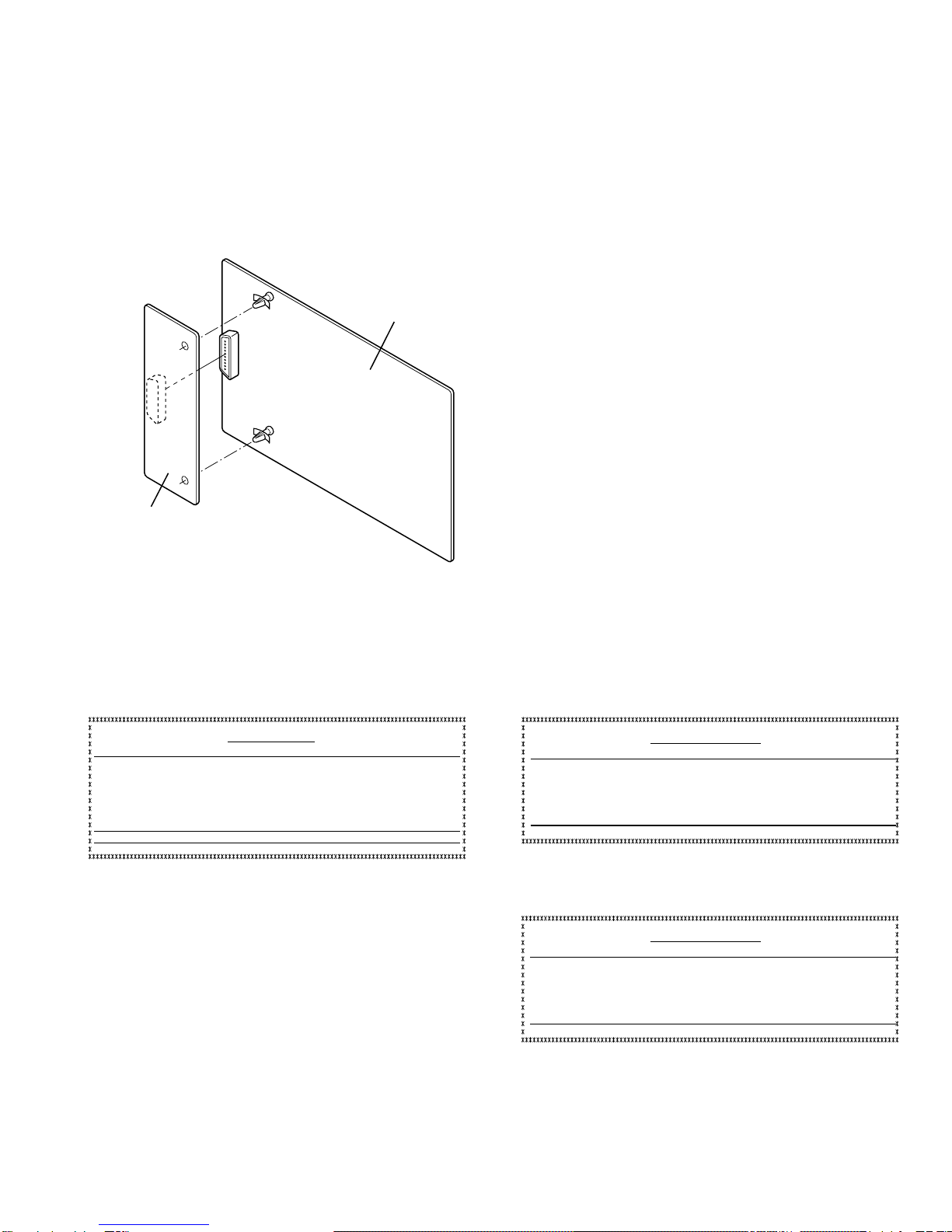
1) Remove the ROM cover of facsimile.
2) Insert two spacers to control PWB, and then connect it to the connec-
tor CNOP of control PWB.
(Fig. 1)
3) Mount the control PWB to which the option memory has been con-
nected in the machine.
(Tighten the screws, and connect the connector without fail.)
4) Mount the ROM cover.
5) After installation turn on the power switch.
appears.
Then, after several seconds,
appears.
PLEASE WAIT A MOMENT
JUN
M:00% STAND BY AUTO
10 MON AM10:00
[3] Diagnostic mode
Successively input "FUNK" + "9" + " " + "8" + "#" + "7". Then,
appears.
After that, press the "START" key.
Then,
appears.
Select MEMORY CLEAR, using the one-touch key "11".
After completion of MEMORY CLEAR,
the following indication appears.
Select ROM/RAM test, using the one-touch key "03".
(This model is provided not only with flash memory for image but also
SRAM to enhance the function to store the number of transmissions
and receptions.)
When the "START" key is pressed again, the memory of machine
(control PWB) and memory of memory unit (excepting the flash mem-
ory) are checked.
An example of indication
After that, the indication shown below appears, and the result table
(Fig. 2) is printed.
After completion of ROM/RAM test the following indication appears.
Then, select the flash memory test, using the one-touch key "12".
In the diagnostic mode perform the image memory (standard, option)
write/read test, as well as complete erase test.
When the "START" key is pressed,
appears, and the indication changes from "–" to "■" whenever data is
written in the flash memory.
After completion of writing of data in all flash memories, the following
indication appears.
After that the long-tone buzzer (normal end) sounds, and at the same
time the following indication appears.
ROM:FAB0
( is ROM
version.)
01:
PRESS START KEY
SOFT SWITCH MODE
03:
PRESS START KEY
ROM RAM CHECK&
ROM CPU SRAM DRM
P P PP
(Upon occurrence of
error "E" appears.)
04:
PRESS START KEY
AUTO FEEDER MODE
12:
PRESS START KEY
FLASH MEMORY
S––E
TEST EXECUTING
SE
TEST EXECUTING
11:
PRESS START KEY
MEMORY CLEAR
12:
PRESS START KEY
FLASH MEMORY
13:
PRESS START KEY
ALL ENTRYFAX/TEL
FO-3MK
– 2 –
Then, the result table (Fig. 3) is printed.
In case of mismatch, the buzzer emits 9 short tones .
After that, the result table (Fig. 4) is output.
1) If any error occurred, check connection of connector CNOP (check
for bending and breakage of pin of connector), check that the option
memory unit has been mounted as specified, and then turn on again
the power supply, and check.
2) If the same error occurs persistently after the measures stated in item
1 above were taken, replace the option memory unit, and check.
3) If the same error occurs again after the measures stated in item 2)
were taken, check the control PWB.
Fig. 1
Fig. 2 Fig. 3
ROM/RAM CHECK LIST
MAIN: ROM =OK
= OK
= OK
= OK
VER.=FAB0X SUM =DE0E
SUM =1C86
VER.=FAB0A
PCU:
SRAM
DRAM
M/C=00
F/W=412250G001J0
CPU
OCT–19–1999 TUE 10:43 AM
FLASH MEMORY = OK (15S, 24S, 27S)
BANKCHANGEOVER = OK
BANK =OK
FLASH MEMORY CHECK REPORT
SIZE=5MB(With Option Flash memory)
OCT–19–1999 TUE 10:45 AM
CNOP
CONTROL PWB
OPTION MEMORY
PWB UNIT
FO-3MK
Fig. 4
FLASH MEMORY = NG (15S, 24S, 27S)
BANKCHANGEOVER = NG
BANK =NG
FLASH MEMORY CHECK REPORT
SIZE=5MB(With Option Flash memory)
OCT–19–1999 TUE 10:45 AM
FO-3MK
1
2
6
4
3
5
BDEFG
I
HCA
BDEFG
I
HCA
1
2
6
4
3
5
4
5
6
7
8
10
11
12
13
17
18
19
20
22
23
24
26
27
28
52
50
47
45
41
39
36
34
51
49
46
44
40
38
35
33
14
2
55
A19
A18
A17
A16
A15
A14
A13
A12
A11
A10
D15
D14
D13
D12
D11
D10
D8
D7
D6
D5
D4
D3
D2
D1
D0
D9
IC4
LH28F800SUT
8Mbit FLASH MEMORY
A20 DQ15
DQ14
DQ13
DQ12
DQ11
DQ10
DQ9
DQ8
DQ7
DQ6
DQ5
DQ4
DQ3
DQ2
DQ1
DQ0
CE0
CE1
/WE
DG
18
16
14
12
9
7
5
3
20
10
/OPMWE
/OPMRD
DG
18
16
14
12
9
7
5
3
20
10
DG
18
16
14
12
9
7
5
3
20
10
DG
25
DGDG
32
53
31
1
16
3
29
30
NC
NC
NC
BYTE
3/5
RP
RY/BY
54
56
15
9
37
43
21
42
48
DG
DGDG
DG
15
14
13
12
11
10
9
7
16
8
DG
FLBK1 1
2
3
6
4
5
A
B
G1
G2A
G2B
C
Y0
Y1
Y3
Y4
Y5
Y6
Y7
Y2
VCC
GND
+5V
/MWRH
/MRD
MA19
MA18
MA17
MA16
MA15
2
4
6
8
11
13
15
17
1
19
1A1
1A2
1A4
2A1
2A2
2A3
2A4
1A3
1G
2G
1Y1
1Y2
1Y4
2Y1
2Y2
2Y3
2Y4
1Y3
VCC
GND
+5V
C113
0.1
D2
HRW0502A
D1
HRW0502A
MA11
MA10
MA9
MA8
MA7
2
4
6
8
11
13
15
17
1
19
1A1
1A2
1A4
2A1
2A2
2A3
2A4
1A3
1G
2G
1Y1
1Y2
1Y4
2Y1
2Y2
2Y3
2Y4
1Y3
VCC
GND
+5V
C110
0.1
MA12
MA13
MA14
CNOP-2
2
4
6
8
11
13
15
17
1
19
1A1
1A2
1A4
2A1
2A2
2A3
2A4
1A3
1G
2G
1Y1
1Y2
1Y4
2Y1
2Y2
2Y3
2Y4
1Y3
VCC
GND C100
0.1
TCS2 R101
4.7K
TCS2
DG
CNOP-7 Vcc 0
CNOP-1
CNOP-9
CNOP-3
CNOP-5
CNOP-50
+5V
+5V +5V +5V +5V
+5V
+5V
+5V
C107
0.1
CNOP-26
CNOP-27
CNOP-28
CNOP-29
CNOP-30
IC1
74HC244
OCTAL BUFFERS
R129 91
R128 91
R127 91
R126 91
R125 91
A19
A18
A17
A16
A15 DG DG
DG
CNOP-32
CNOP-31
CNOP-33
CNOP-34
CNOP-35
CNOP-36
CNOP-37
CNOP-38
R124 91
R123 91
R122 91
R121 91
R120 91
A14
A13
A12
A11
A10
R119 91
R118 91
R117 91
A9
A8
A7
IC2
74HC244 OCTAL BUFFERS
IC3
74HC244 OCTUL BUFFERS
R115 91
R114 91 A5
A4
R113 91
R112 91
R111 91
A3
A2
A1
R116 91 A6
DG
MA5
MA4
MA3
MA2
MA1
MA6
CNOP-39
CNOP-40
CNOP-41
CNOP-42
CNOP-43
CNOP-44
GND 0
C10
22/16 C106
0.1
C9
22/16
C105
0.1
+5V
A[19:0]
CNOP-45
FLBK4
R100
A9
A8
A7
A6
A5
A4
A3
A2
A1
A19
A18
A17
A16
A15
A14
A13
A12
A11
A10
A9
A8
A7
A6
A5
A4
A3
A2
A1
A0
/OE
/FLS0
/OPMWE
/OPMRD
/FLBSY
TCS2
WP
VPP
VCC
VCC
VCC
GND
GND
GND
GND 0
Vcc 0
R102
0
C116
0.1
C118
0.1
C101
0.1 C102
0.1 C4
22/16
FLBK2
FLBK3
CNOP-47
CNOP-46
CNOP-49
CNOP-48 /FLOPT
/FLS0
/FLS1
/FLS2
/FLS3
/FLS4
/FLS5
/FLS6
/FLS7
IC6
74HC138
3-TO-8 LINE DECORDERS
4
5
6
7
8
10
11
12
13
17
18
19
20
22
23
24
26
27
28
52
50
47
45
41
39
36
34
51
49
46
44
40
38
35
33
14
2
55
A19
A18
A17
A16
A15
A14
A13
A12
A11
A10
D15
D14
D13
D12
D11
D10
D8
D7
D6
D5
D4
D3
D2
D1
D0
D9
IC5
LH28F016SUT
16Mbit FLASH MEMORY
A20 DQ15
DQ14
DQ13
DQ12
DQ11
DQ10
DQ9
DQ8
DQ7
DQ6
DQ5
DQ4
DQ3
DQ2
DQ1
DQ0
CE0
CE1
/WE
25
32
53
31
1
16
3
29
30
NC
NC
NC
BYTE
3/5
RP
RY/BY
54
56
15
9
37
43
21
42
48
FLBK4
A9
A8
A7
A6
A5
A4
A3
A2
A1
A19
A18
A17
A16
A15
A14
A13
A12
A11
A10
A9
A8
A7
A6
A5
A4
A3
A2
A1
A0
/OE
WP
VPP
VCC
VCC
VCC
GND
GND
GND
CNOP-45
TCS2
/FLBSY
CNOP-8
(*2) /FLBSY
+5V
R103
4.7K
DG
/FLS1
/OPMWE
/OPMRD
GND 0
Vcc 0
R104
0
C120
0.1
C122
0.1 C103
0.1 C104
0.1 C6
22/16
CNOP-15
CNOP-16
CNOP-17
CNOP-18
CNOP-19
CNOP-10
CNOP-11
CNOP-12
CNOP-13
CNOP-14
CNOP-20
CNOP-21
CNOP-22
CNOP-23
CNOP-24
CNOP-25
D15
D14
D13
D12
D11
D10
D8
D7
D6
D5
D4
D3
D2
D1
D0
D9
D[15:0]
DG
+5V
DG
(2-6A)
(3-5E)
(3-5E)
(3-5E)
(*1)
(*1)
(1-3F)
(1-2B)
(1-3C)(1-3F)(2-1A)
(2-1C)(2-1E)(2-4A)
(2-4D)(2-4F)
(1-2E)
(1-5C)
(1-5C)
(*2) : (1-3C)(1-3F)
(2-1A)(2-1C)
(2-1E)(2-4A)
(2-4D)(2-4F)
(*2)
(1-2B)
(3-5B)(3-5F)
(1-2E)
(1-5C)
(1-5C)
(1-4E)
(1-4H)
(2-4C)
(2-4E)
(2-4G)
(2-2C)
(2-2E)
(2-2G)
(*1) : (1-3E)(1-3H)(2-2C)(2-2E)
(2-2G)(2-4C)(2-4E)(2-4G)
N.M.
– 3 –
[4] Circuit schematics and parts layout
Option memory PWB circuit 1/3
FO-3MK
– 4 –
1
2
6
4
3
5
BDEFG
I
HCA
BDEFG
I
HCA
1
2
6
4
3
5
4
5
6
7
8
10
11
12
13
17
18
19
20
22
23
25
26
27
52
50
47
45
41
39
36
34
51
49
46
44
40
38
35
33
14
2
A19
A18
A17
A16
A15
A14
A13
A12
A11
D14
D13
D12
D10
D9
D8
D7
D6
D5
D4
D3
D2
A10
A9
A8
A7
A6
D11
IC7
LH28F016SUT
16Mbit FLASH MEMORY
A20
A19
A18
A17
A16
A15
A14
A13
A12
A11
A10
A9
A8
A7
A6
A4
A3
A2
DQ15
DQ14
DQ13
DQ12
DQ11
DQ10
DQ9
DQ8
DQ7
DQ6
DQ5
DQ4
DQ3
DQ2
DQ1
DQ0
CE0
CE1
A5
A4
A3
A2
A1
24
28
A5
A1
A0
D15
D1
D0
RY/BY
BYTE
3/5
RP
NC
NC
NC
/OE
/WE
WP
VCC
VPP
VCC
VCC
GND
GND
GND
55
54
56
15
9
37
43
21
42
48
32
53
31
1
16
3
29
30 DG
R105
0
C124
0.1
C126
0.1 C108
0.1 C109
0.1
GND 0
Vcc 0
4
5
6
7
8
10
11
12
13
17
18
19
20
22
23
25
26
27
52
50
47
45
41
39
36
34
51
49
46
44
40
38
35
33
14
2
A19
A18
A17
A16
A15
A14
A13
A12
A11
D14
D13
D12
D10
D9
D8
D7
D6
D5
D4
D3
D2
A10
A9
A8
A7
A6
D11
A20
A19
A18
A17
A16
A15
A14
A13
A12
A11
A10
A9
A8
A7
A6
A4
A3
A2
DQ15
DQ14
DQ13
DQ12
DQ11
DQ10
DQ9
DQ8
DQ7
DQ6
DQ5
DQ4
DQ3
DQ2
DQ1
DQ0
CE0
CE1
A5
A4
A3
A2
A1
24
28
A5
A1
A0
D15
D1
D0
RY/BY
BYTE
3/5
RP
NC
NC
NC
/OE
/WE
WP
VCC
VPP
VCC
VCC
GND
GND
GND
55
54
56
15
9
37
43
21
42
48
32
53
31
1
16
3
29
30 DG
R108
C132 C133 C117 C119
GND 0
Vcc 0
DG
DG
4
5
6
7
8
10
11
12
13
17
18
19
20
22
23
25
26
27
52
50
47
45
41
39
36
34
51
49
46
44
40
38
35
33
14
2
A19
A18
A17
A16
A15
A14
A13
A12
A11
D14
D13
D12
D10
D9
D8
D7
D6
D5
D4
D3
D2
A10
A9
A8
A7
A6
D11
IC8
A20
A19
A18
A17
A16
A15
A14
A13
A12
A11
A10
A9
A8
A7
A6
A4
A3
A2
DQ15
DQ14
DQ13
DQ12
DQ11
DQ10
DQ9
DQ8
DQ7
DQ6
DQ5
DQ4
DQ3
DQ2
DQ1
DQ0
CE0
CE1
A5
A4
A3
A2
A1
24
28
A5
A1
A0
D15
D1
D0
RY/BY
BYTE
3/5
RP
NC
NC
NC
/OE
/WE
WP
VCC
VPP
VCC
VCC
GND
GND
GND
55
54
56
15
9
37
43
21
42
48
32
53
31
1
16
3
29
30 DG
R106
C128
C129 C111 C112
GND 0
Vcc 0
4
5
6
7
8
10
11
12
13
17
18
19
20
22
23
25
26
27
52
50
47
45
41
39
36
34
51
49
46
44
40
38
35
33
14
2
A19
A18
A17
A16
A15
A14
A13
A12
A11
D14
D13
D12
D10
D9
D8
D7
D6
D5
D4
D3
D2
A10
A9
A8
A7
A6
D11
A20
A19
A18
A17
A16
A15
A14
A13
A12
A11
A10
A9
A8
A7
A6
A4
A3
A2
DQ15
DQ14
DQ13
DQ12
DQ11
DQ10
DQ9
DQ8
DQ7
DQ6
DQ5
DQ4
DQ3
DQ2
DQ1
DQ0
CE0
CE1
A5
A4
A3
A2
A1
24
28
A5
A1
A0
D15
D1
D0
RY/BY
BYTE
3/5
RP
NC
NC
NC
/OE
/WE
WP
VCC
VPP
VCC
VCC
GND
GND
GND
55
54
56
15
9
37
43
21
42
48
32
53
31
1
16
3
29
30
DG
R109
C134
C135
C121
C123
GND 0
Vcc 0
4
5
6
7
8
10
11
12
13
17
18
19
20
22
23
25
26
27
52
50
47
45
41
39
36
34
51
49
46
44
40
38
35
33
14
2
A19
A18
A17
A16
A15
A14
A13
A12
A11
D14
D13
D12
D10
D9
D8
D7
D6
D5
D4
D3
D2
A10
A9
A8
A7
A6
D11
IC9
A20
A19
A18
A17
A16
A15
A14
A13
A12
A11
A10
A9
A8
A7
A6
A4
A3
A2
DQ15
DQ14
DQ13
DQ12
DQ11
DQ10
DQ9
DQ8
DQ7
DQ6
DQ5
DQ4
DQ3
DQ2
DQ1
DQ0
CE0
CE1
A5
A4
A3
A2
A1
24
28
A5
A1
A0
D15
D1
D0
RY/BY
BYTE
3/5
RP
NC
NC
NC
/OE
/WE
WP
VCC
VPP
VCC
VCC
GND
GND
GND
55
54
56
15
9
37
43
21
42
48
32
53
31
1
16
3
29
30 DG
R107
C130 C131 C114 C115
GND 0
Vcc 0
4
5
6
7
8
10
11
12
13
17
18
19
20
22
23
25
26
27
52
50
47
45
41
39
36
34
51
49
46
44
40
38
35
33
14
2
A19
A18
A17
A16
A15
A14
A13
A12
A11
D14
D13
D12
D10
D9
D8
D7
D6
D5
D4
D3
D2
A10
A9
A8
A7
A6
D11
A20
A19
A18
A17
A16
A15
A14
A13
A12
A11
A10
A9
A8
A7
A6
A4
A3
A2
DQ15
DQ14
DQ13
DQ12
DQ11
DQ10
DQ9
DQ8
DQ7
DQ6
DQ5
DQ4
DQ3
DQ2
DQ1
DQ0
CE0
CE1
A5
A4
A3
A2
A1
24
28
A5
A1
A0
D15
D1
D0
RY/BY
BYTE
3/5
RP
NC
NC
NC
/OE
/WE
WP
VCC
VPP
VCC
VCC
GND
GND
GND
55
54
56
15
9
37
43
21
42
48
32
53
31
1
16
3
29
30
DG
R110
C136 C137 C125 C127
GND 0
Vcc 0
/FLS6
/OPMWE
/OPMRD
C5 C7
C3
N.M.
/FLS5
/OPMWE
/OPMRD
/FLS7
/OPMWE
/OPMRD
/FLS2
/OPMWE
/OPMRD
/FLS3
/OPMRD
/OPMWE
/FLS4
/OPMWE
/OPMRD
C1 C2
IC10 IC11
/FLBSY
TCS2 DG
DG
DG
DG
/FLBSY
TCS2
/FLBSY
TCS2
CNOP-45
CNOP-45
CNOP-45
/FLBSY
TCS2
DG
DG
DG
DG
DG
DG
+5V +5V
/FLBSY
TCS2
+5V
/FLBSY
TCS2
+5V
+5V
+5V
+5V
+5V
+5V
+5V
+5V +5V
+5V +5V
+5V
+5V +5V
+5V
D[15:0]
A[19:0]
FLBK4
C8
22/16
FLBK4
FLBK4
FLBK4
FLBK4
FLBK4
CNOP45
IC12
(1-3F)
(1-2B)
(1-2E)
(1-5C)
(1-5C)
(1-3F)
(1-2B)
(1-2E)
(1-5C)
(1-5C)
(1-3F)
(1-2B)
(1-2E)
(1-5C)
(1-5C)
(1-3F)
(1-2B)
(1-2E)
(1-5C)
(1-5C)
(1-2E)
(1-5C)
(1-5C)
(3-5B)
(3-5F)
(1-3F)
(1-2B)
(1-2E)
(1-5C)
(1-5C)
(1-3F)
(1-2B)
(1-5B)
N.M.
CNOP45 CNOP45
Option memory PWB circuit
2/3
FO-3MK
– 5 –
1
2
6
4
3
5
BDEFG
I
HCA
BDEFG
I
HCA
1
2
6
4
3
5
DG
DG
+5V
+5V
D14
D12
D10
D8
D6
D4
D2
D0
MA18
MA16
MA14
MA12
MA10
MA8
MA6
MA4
MA2
FLBK4
FLBK1
FLBK3
DG
TCS2
/MWRH
/MRD
/FLBSY
D15
D13
D11
D9
D7
D5
D3
D1
MA19
MA17
MA15
MA13
MA11
MA9
MA7
MA5
MA3
MA1
FLBK2
/FLOPT
DG
1
3
7
9
11
13
15
17
19
21
23
25
27
5
29
31
35
37
39
41
43
45
47
49
33
2
4
8
10
12
14
16
18
20
22
24
26
28
6
30
32
36
38
40
42
44
46
48
50
34
DG
+5V
DG
FLBK4
FLBK1
FLBK3
TCS2
CNOP
/MWRH
/MRD
/FLBSY
FLBK2
/FLOPT
(1-6H)(2-6H)
(1-3~5A)
(1-5D)(1-5F)(2-3A)(2-3C)(2-3F)
(2-5A)(2-5D)(2-5F) (1-2D)
(1-2D)
(1-2D)
(1-1D)
(1-3~5A)
(1-6H)(2-6H)
(1-2A)
(1-5A)
(1-5A)
(1-3F)
Option memory PWB circuit 3/3
FO-3MK
Option memory PWB parts layout (Top side)
Option memory PWB parts layout (Bottom side)
– 6 –
FO-3MK
[1] Packing parts
1 SPAKA110BXHZZ AB D Vinyl bag
2 SSAKA0006UCZZ AA D Vinyl bag
3 LSTY-0057AFZZ AC C Spacer
4 SPAKC285BXHZZ AD N D Packing case
5 PSHEM3490XHZZ AC D Aluminum foil
[2] Option memory PWB unit
1 VCEAPS226AF1C AC C Capacitor(16WV 22µF) [C4]
2 VCEAPS226AF1C AC C Capacitor(16WV 22µF) [C6]
3 VCEAPS226AF1C AC C Capacitor(16WV 22µF) [C8]
4 VCEAPS226AF1C AC C Capacitor(16WV 22µF) [C9]
5 VCEAPS226AF1C AC C Capacitor(16WV 22µF) [C10]
6 VCKYTV1EF104Z AA C Capacitor(25WV 0.1µF) [C100]
7 VCKYTV1EF104Z AA C Capacitor(25WV 0.1µF) [C101]
8 VCKYTV1EF104Z AA C Capacitor(25WV 0.1µF) [C102]
9 VCKYTV1EF104Z AA C Capacitor(25WV 0.1µF) [C103]
10 VCKYTV1EF104Z AA C Capacitor(25WV 0.1µF) [C104]
11 VCKYTV1EF104Z AA C Capacitor(25WV 0.1µF) [C105]
12 VCKYTV1EF104Z AA C Capacitor(25WV 0.1µF) [C106]
13 VCKYTV1EF104Z AA C Capacitor(25WV 0.1µF) [C107]
14 VCKYTV1EF104Z AA C Capacitor(25WV 0.1µF) [C108]
15 VCKYTV1EF104Z AA C Capacitor(25WV 0.1µF) [C109]
16 VCKYTV1EF104Z AA C Capacitor(25WV 0.1µF) [C110]
17 VCKYTV1EF104Z AA C Capacitor(25WV 0.1µF) [C113]
18 VCKYTV1EF104Z AA C Capacitor(25WV 0.1µF) [C116]
19 VCKYTV1EF104Z AA C Capacitor(25WV 0.1µF) [C118]
20 VCKYTV1EF104Z AA C Capacitor(25WV 0.1µF) [C120]
21 VCKYTV1EF104Z AA C Capacitor(25WV 0.1µF) [C122]
22 VCKYTV1EF104Z AA C Capacitor(25WV 0.1µF) [C124]
23 VCKYTV1EF104Z AA C Capacitor(25WV 0.1µF) [C126]
24 QCNCW2590SC5J AM C Connector(50pin) [CNOP]
25 VHDHRW0502A-1 AD B Diode(HRW0502A) [D1]
26 VHDHRW0502A-1 AD B Diode(HRW0502A) [D2]
27 VHIHD74HC244F AE B IC(HD74HC244), OCTAL BUFFERS [IC1]
28 VHIHD74HC244F AE B IC(HD74HC244), OCTAL BUFFERS [IC2]
29 VHIHD74HC244F AE B IC(HD74HC244), OCTAL BUFFERS [IC3]
30 VHILH28F80S10 BH B IC(LH28F800SUT), 8Mbit FLASH MEMORY [IC4]
31 VHILH28F016SU BR B IC(LH28F016SUT), 16Mbit FLASH MEMORY [IC5]
32 VHIHD74HC138F AE B IC(HD74HC138), 3–TO–8 LINE DECORDERS [IC6]
33 VHILH28F016SU BR B IC(LH28F016SUT), 16Mbit FLASH MEMORY [IC7]
34 VRS-TS2AD472J AA C Resistor(1/10W 4.7KΩ±5%) [R101]
35 VRS-TS2AD000J AA C Resistor(1/10W 0Ω±5%) [R102]
36 VRS-TS2AD472J AA C Resistor(1/10W 4.7KΩ±5%) [R103]
37 VRS-TS2AD000J AA C Resistor(1/10W 0Ω±5%) [R104]
38 VRS-TS2AD000J AA C Resistor(1/10W 0Ω±5%) [R105]
39 VRS-TS2AD910J AA C Resistor(1/10W 91Ω±5%) [R111]~[R129]
(Unit)
901 DCEKM473BXH03 BR N E Option memory PWB unit
[5] Parts guide
NO. PARTS CODE PRICE
RANK NEW
MARK PART
RANK DESCRIPTION
SHARP CORPORATION
Communication Systems Group
Quality & Reliability Control Center
Higashihiroshima, Hiroshima 739-0192, Japan
Printed in Japan
9911-1834SS•IS•T
No part of this publication may be reproduced,
stored in a retrieval system, or transmitted in
any form or by any means, electronic, mechanical,
photocopying, recording, or otherwise, without
prior written permission of the publisher.
COPYRIGHT © 1999 BY SHARP CORPORATION
ALL RIGHTS RESERVED.

This manual suits for next models

1

Other Sharp Printer Accessories manuals

Sharp AR-NS1 User manual

Sharp

Sharp AR-NS1 User manual

Sharp AR-FR11 User manual

Sharp

Sharp AR-FR11 User manual

Sharp AR-PB2A User manual

Sharp

Sharp AR-PB2A User manual

Sharp AR-FX12 User manual

Sharp

Sharp AR-FX12 User manual

Sharp FO-59A4 Instruction Manual

Sharp

Sharp FO-59A4 Instruction Manual

Sharp AM-300 User manual

Sharp

Sharp AM-300 User manual

Sharp MX-CFX1 User manual

Sharp

Sharp MX-CFX1 User manual

Sharp MX-FR46U User manual

Sharp

Sharp MX-FR46U User manual

Sharp MX-FX12 Guide

Sharp

Sharp MX-FX12 Guide

Sharp AR-NB2 User manual

Sharp

Sharp AR-NB2 User manual

Sharp AR-RB1 User manual

Sharp

Sharp AR-RB1 User manual

Sharp AR-PB2A User manual

Sharp

Sharp AR-PB2A User manual

Sharp SF-461 User manual

Sharp

Sharp SF-461 User manual

Sharp AR-FR11U User manual

Sharp

Sharp AR-FR11U User manual

Sharp AR-S11 User manual

Sharp

Sharp AR-S11 User manual

Sharp AR-F14 User manual

Sharp

Sharp AR-F14 User manual

Sharp AR-P15 User manual

Sharp

Sharp AR-P15 User manual

Sharp FO-1MK User manual

Sharp

Sharp FO-1MK User manual

Sharp AR-FN7 User manual

Sharp

Sharp AR-FN7 User manual

Sharp ARNC5J User manual

Sharp

Sharp ARNC5J User manual

Sharp AR-NB3 User manual

Sharp

Sharp AR-NB3 User manual

Sharp AR-DU3 User manual

Sharp

Sharp AR-DU3 User manual

Sharp AR-D28 User manual

Sharp

Sharp AR-D28 User manual

Sharp AR-NB2 User manual

Sharp

Sharp AR-NB2 User manual

Popular Printer Accessories manuals by other brands

Intermec PB2 Series supplementary guide

Intermec

Intermec PB2 Series supplementary guide

Xerox 3R11500 Specifications

Xerox

Xerox 3R11500 Specifications

Roland ZEC-U5032 reference guide

Roland

Roland ZEC-U5032 reference guide

Intermec 3600 instruction sheet

Intermec

Intermec 3600 instruction sheet

Star Micronics TCP300 Series install guide

Star Micronics

Star Micronics TCP300 Series install guide

HP Smart Tank Wireless 450 Series manual

HP

HP Smart Tank Wireless 450 Series manual

Epson T069420 Product information sheet

Epson

Epson T069420 Product information sheet

GE Interlogix Calibur CBR-PB3-WD installation guide

GE Interlogix

GE Interlogix Calibur CBR-PB3-WD installation guide

Fujitsu PA03753-0002 Consumable replacement and cleaning instructions

Fujitsu

Fujitsu PA03753-0002 Consumable replacement and cleaning instructions

HP DesignJet 5000 cp Specifications

HP

HP DesignJet 5000 cp Specifications

Xerox Versant 4100 Press manual

Xerox

Xerox Versant 4100 Press manual

Xerox Phaser 6300/DN Accessories guide

Xerox

Xerox Phaser 6300/DN Accessories guide

Canon Two-Knife Booklet Trimmer-A1 Service manual

Canon

Canon Two-Knife Booklet Trimmer-A1 Service manual

Kyocera ECOSYS FS-1350DN user guide

Kyocera

Kyocera ECOSYS FS-1350DN user guide

Triumph Adler Utax PF 770 Service manual

Triumph Adler

Triumph Adler Utax PF 770 Service manual

Epson T602600 Material safety data sheet

Epson

Epson T602600 Material safety data sheet

Xerox Phaser 6180MFP instruction sheet

Xerox

Xerox Phaser 6180MFP instruction sheet

Konica Minolta bizhub C220 Series user guide

Konica Minolta

Konica Minolta bizhub C220 Series user guide

manuals.online logo
manuals.online logoBrands
  • About & Mission
  • Contact us
  • Privacy Policy
  • Terms and Conditions

Copyright 2025 Manuals.Online. All Rights Reserved.