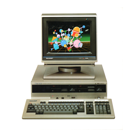
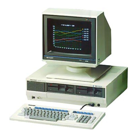
Sharp MZ-700 Series User manual

MZ-700
SERVICE MANUAL
-r'
.............................................................
..
SHARP
INDEX
CODE: OOZMZ700SM
I/
E
PERSONAL COMPUTER
MODEL
MZ-700
MZ-1TOl
MZ-1POl
(FOR THE MZ-lPOI MECHANICAL SECTION
REFER
TO
THE DPG2306 SERVICE MANUAL)
1.
SPECIFICATIONS.
. . . . . . . . . . . . . . . .
..
. . . . .
..
. . . . .
..
. .
..
. .
..
1
2.
NAMES OF
FUNCTIONAL
COMPONENTS. . . . . . . . . . . . . . . . . . .
..
2
3.
SYSTEM BLOCK
DIAGRAM
..............................
_
..
3
4. SYSTEM
DESCRIPTION.
. . . . . . . . . . . . •. . . . . . . . . . . . .
•.
. . . . .
..
4
5.
DATA
RECORDER
....................................
....
15
6.
COLOUR ENCODER
.......
.
........
. .
..
......
.
............
19
7.
MICRO COLOUR GRAPHIC PRINTER
.........................
20
8.
POWER
SUPPLy
...................
.
.............
•
........
24
9.
IC
SIGNAL
POSITION
.......................•...........
. . 27
10.
CIRCUIT
DIAGRAM
& PARTS
LAyOUT
...•.
..
...
..
....
..
....
29
11.
PARTS GUIDE & LIST
SHARP
CORPORATION

~\~Z~
700
1.
SPECIFICATION
1-1.
MZ-700
CPU
Oock(ct»
Memory
Video
output
Screen structure
Color designation
Music function
Timepiece
function
Keyboard
Editing functions
Power
requirements
Temperature
Humidity
Weight
Physical
dimensions
Sharp LH0080A (Z-80A)
3.5MHz
4KB ROM (monitor)
4KB ROM (character generator)
64KB RAM (program area)
4KB RAM (VIDEO)
System: PAL
Type: RGB composite video (con-
vertible
to
B/W)
RCB + Syncronization
(non
composite)
RF
(UHF
36
± 3ch, conver-
tible
to
B/W)
40
character x 25 lines
(1000
chara-
cters)
8 x 8
dot
matrix
(per
character)
Character: 8 colours
(per
character)
Background: 8 colours (per character)
Internally provided (audio
output,
55OmVmax.)
Internally provided
(24
hours clock,
without data retention)
ASCII compatible
69
keys
Defmable keys,cursorcontrolkeys, etc.
Screen editor (cursor control, home,
clear, insert, delete)
220/240V ± 10V, SO/60Hz
Operating temperature: 0
to
35°C
Storage temperature:
-20
to
70°C
Operating humidity: 85%RH or
below
3.6Kg
(body
only)
440
(W) x 305 (D) x
86
(H)
1-2. CPU board specification
CPU
LH0080A (Z80A) . . . . . . . .
..
I
PlO 8255
..................
I
CTC 8253
...................
I
Memory controller M60719
................
I
(CRTC)
ROM
RAM
I/O bus
4KB
monitor
ROM . . . . . . . . .
..
I
4KB character generator
ROM
...
I
64K bits DRAM . . . . . . . . . . .
..
8
2KB SRAM
................
2
Expansion I/O bus
...........
I
Printer I/O bus . . . . . . . . . . . .
..
2
(Only one can be used, selectable
by
switching)
External cassette read/write terminals
1-3. Micro-colour graphics printer specification (option)
Printing method Ball point pen recording, four colours
rotary selection type.
Kind
of
colours I =black, 2 =blue, 3 =green, 4= red
Printingspeed
10
characters/sec, average (Printing the
smallest characters.)
Printing capacity
80
digits,
40
digits, 26 digits, soft-
ware designated
Character set 115 characters (ASCII characters and
others)
Resolution 0.2mm
1-4. Cassette recorder specification (option)
Type IEC compatible cassette mechanism
Record/playback
method
Dual tracks, single channel, monopho-
nic
Rated speed 4.8cm/±3.5%
Operation control
method Piano key
method
Control
buttons
PLAY,
FF,
REW, STOP/EJECT, REC,
COUNTER RESET
Data transfer .
system
Baud rate
Tape
used
Sharp,
PWM
method
1200bps(nominal)
Philips standard tape,
(not
C120)
1-5.
Powersupply specification
(Including colour graphics printer and cassette tape
power source)
Input:
220/24OV ± 10V, 60/50Hz, 20W
Output:
5V

2.
NAME
OF
FUNCTIONAL
COMPONENT
MZ-700 Front view
Main
kev
board
-----'
MZ-700
Aeer
view
Channel switch
RF
terminal
BrN-Colour
switch
Composi!
terminal
Dat8 recorder
!c3S$IIttll)
AGe
terminal
CantUI!
re<:order
jKk
EKt.
output
terminal
Joy
nick
ulfminal
1
plOHtr
printer
Ext.
printer
terminal
MZ-700
plolter
prioter
recorder (cassette)
INS.
DEL
key
":::d'---,----CUrSOI
control
keV$
.
socket
Reset switch
Volume
Adiust
F,.me
ground
termmal

~"q-700
3. SYSTEM BLOCK DIAGRAM
( CRT
F.G
A.C.
sw
100V
I~
-""
t t
~PO~UP'
!II
0-
5V
MEMORY CONTRa.
Fi
p w R.G.B. I I
PLY CIRCUIT
llER
(CRTC)
VIDEO
RAM
a::
Cl
-..,
I I
,.--
:Ja::
00
RF I I
~
~~
...JU
oz
-uw
_J
I
eJ
Reset
RESET 1
~
~
I
CHAR
a::
VIDEO
CIRCUITJ I GEN
....
...J
sw
c(
MAIN
~
MEMORY
64KB
DRAM
MONITOR
ROM
Z80A
i-
III
IT
CPU
A
,......
\ ADDRESS
BUS
\
I
n I
n=
-y
en
:J
A "
III
~dJA
\
Q.
I -
"
ft
H
rn.
t\.0
-t "
a:
..
X
(ONTROl
BUS
I--
. w
...-
>
I--
...
~I
?8m
ER!-
f--
I--
I--
'--
r
f--
~
t
!.
8253 (CTC)
r-
8255 (PlO)
EMPO
CO
C1
C2
CONTROLLER
t,;J~
">
0(
CASSET·
Audio TEMPO. +
f..--
KEY I
TECONT·
11
JOY STICK1
amp. CURSOR
OSC.
BOARD ROLLER CIRCUIT
I
~
I--
t
PRINTER
CONTROL
LER
~
r "\
PRINTER BUS J
CASSETTE JOY STICK
TERMINAL
TERMINAL
~
U U I
CASSETTE
3

4.
SYSTEM
DESCRIPTION
4-1.
Memory map
a) At power
on
$0000
$1000
$1200
$0000
$0800
$EOoo
$FOoo
MONITOR
(ROM)
MONITOR WORK
SYSTEM
and
TEXT
AREA
(DRAM)
V·RAM<CHARACTER>
(SRAMI
V·RAM<COLORDATA>
(SRAMI
KEY
and
TIMER
PORT
FLOPPY CONTROLLER
Enable
$0000
$1000
$0000
SYSTEM
(DRAM)
and
TEXT
AREA
SYSTEM
and
TEXT
AREA
(DRAM)
Disable
• Shown above
is
the memory map at the time
of
power
on.
VRAM
contents from$DOOO to $DFFF differ from
the MZ·80K.
• The monitor (ROM) has the same entry point
as
that
of
the MZ·80K.
b) Bootstrap (loading
of
system program)
$0000 $0000
MONITOR
Ir--
(ROfv\)
1'-
SYSTEM
$1000 LOAD
SYSTEM
$7EOD
Boot PROGRAM
~
'11
$0000
$0000
V·RAM
V·RAM
$EOoo
KEY and
TIMER
PORT
SYSTEM
Eneble Disable
• With the input
of
the LOAD command
of
the monitor,
the
BASIC
loading program
is
transferred
to
the system
area composed
of
the
RAM
and starts
to
bootstrap.
(Only the cassette tape
is
subject
to
bootstrapping in
this case).
4
• Boot command: L
• With the entry
of
the boot command
L,
only the tape
loading program
is
transferred
to
the system area and the
system program
is
loaded
to
the system area designated
in the DRAM.
NOTE: The boot program shown in the figure
is
the
program loaded from the tape and
is
not the
program from the monitor (ROM).
c) System initiation
$0000
$1000
MONITOR
(ROM)
.$0000
,-------,
V·RAM
V·RAM
$Eooo I--KE-Y-ond-TI-M-ER-P-OR-T-l
:$Fooo
1--------1
Disable
$0000
,-----,
SYSTEM
$1000 ----------------------
$0000
---------------------------
Enable
• The above memory map is valid upon completion
of
system program loading.
• The system program
is
programmed
to
switch the
memory depending upon what
is
accessed,
VRAM,
keyboard, or timer.
d) At
the
time
of
manual reset
$0000
$1000
MONITOR
(ROM) $0000 I SYSTEM
$1000
~-----~
SYSTEM
$0000
$0000
,-------,
V·RAM
V-RAM
$EOoo
KEY
and
TIMER
PORT
SYSTEM
$FOoo
Enable Disable

~1Z
-7CO
At the time
of
manual reset (with I
CTRL
I in depression)
$0000
$0000
SYSTEM
~
MONITOR
-
(ROM)
$1000
$1000
SYSTEM
$0000
$0000
V-RAM
V-RAM
$EOoo
KEY
and
TIMER
PORT
SYSTEM
$FOOO
~
MEMORYCHANGE
'--
Disable Enable
•
When
the IC T R L Ikey
is
in depression, address $0000
through $OFFF and
$DOOO
through $FFFF become
the
RAM
area.
• With input
of
the command ":If' when the monitor
(ROM)
is
active, it
is
switched
to
the
RAM.
e) Floppy bootstrap
$0000
....--------,
MONITOR
(ROM)
$1000
f----------I
SYSTEM
iI-
Iv
$DOOO~----~
V-RAM
V-RAM
$EOoo
i-
K
-E-y -an-dT-IM-E-R-PO-R-l
-I
$FOoo
f----------I
FLOPPYCONTRO~L-
Enable
$0000 I SYSTEM
$1000
~----~
LOAD
$0000
,------,
SYSTEM
Disable
• Because the floppy control area
is
mapped to
$FOOO
for
compatibility with the MZ-80K series, boot begins
from the adress
$FOOO.
•
Map
configuration after boot will
be
considered sepa-
rately.
4-2. Memory controller (CRT
C)
Both the momory controller and the CRT controller
are
contained in a
single
chip custom
LSI
(M60719), it
has the following functions:
5
a.
8 x 8 dot characters are displayed on the CRT screen
of
40
characters (horizontal) x 25 lines (vertical). Displayed
character font
is
dependent on the
4KB
character
generator (ROM).
b.
Manages
the monitor
ROM,
DRAM, video
RAM,
and
peripherals (keyboard, timer, ETC.) mapped to the
memory.
c.
Generates clock to the Z-80A microprocessor.
d.
Selects the printer I/O port.
1) CRT controller
There are major variations
of
colour television systems
as
described below.
1.
NTSC
system (Japan, U.S.A., etc.)
2. PAL system (U.K., Germany, etc.)
3.
SECAM
system (French, etc.)
Because
of
the different specification requirements above,
the
MZ-
700 may not be suitable for overseas operation.
PALsignal specification
Signal name Signal frequency
NTPL
"L"
LPHI 17.734475
MHz
CLKN 8.8672375
MHz
COLR 4.43361875
MHz
WAD
1.108404688
MHz
PHIO 3.546875
MHz
HBLN
15.6113 kHz
VBLN 50.0363
Hz
CRT
controller
system
block
diagram
H
NTPL
CPU
WA
CPU
Blanking period
COLR
HSY
SYN
VBLK
HBLK
CLK
LOAD
TV
Oata written in
the
VAAM
from
the
CPU
is
input
to
01-08
via
the
bidirectional
buffer
5245.
To display characters on the CRT screen, the
CPU
writes
the character data (display code) to the
2KB
VRAM-l
along with the control signal
WR
and the color data
of
that character
to
the
2KB
VRAM-
2.
In other words,
as
the address
($DOOO
,..,
$D7FF)
is
output. The character
data
is
supplied to the VRAM-l input (01-08)
via
the bidirectional buffer LS245, and the data will then
be written when
WE
is
low. The color data
is
also sent to
01-08
of
the
VRAM-2
to be written when
WE
is
low.
To read the contents
of
a
VRAM
character, the
CPU
sends
out
the relevant address. When
RD
is forced low, the
data
is
then read
via
the bidirectional buffer LS245.
However, the address range
$0000
through $DFFF must
be addressed in order to access
all
the
VRAM.
This address
change
is
carried
out
inside the custom
LSI
with the OUT
command described later.
Accessing
of
the
VRAM
is carried
out
within the blinking
period (BLNK = "H").
If
BLNK =
"L",
then
WAIT
is
applied to the
CPU
(WA
= "L").
The blanking period discussed here
is
the period that
BLNK
is
in high level.
High
period
of
the BLNK signal
is
so
designed that it
is
shorter than the low period
of
HBLK (horizontal blanking
period).
HBLK
versus
BLNK
HBLK~
,
BLNK--,L.
____________
~--~I
!
~
I:
L"I----
, 1
I'
-:
l--
2.165081-1S
Display period
The data written in the
VRAM
is
sent
to
the
CG
ROM,
character
by
character based on the display address counter
located inside the custom LSI, to become the
CG
address
data (VRAM-l data). Also, the data
of
VRAM-2
is
sent
to the LS174, at this point. The
CG
receives the VRAM-l
data and low order address bits (Q-Q3).
It
is
then sent to
the shift register LS165 after being converted into the
8-bit parallel character row data. The shift register converts
this signal into serial data and it
is
added to the color
matrix circuit along with the data from the LS174 to
become the R.G.B. CVIDEO signal.
Po
-PlO: These are
VRAM
addresses
that
represent the
character position
on
the CRT screen.
Ql -Q3: These represent the rows
of
the 8 x 8 dot
character. Row number
is
increased with
HBLK,
and it repeats 0 through 7
as
shown
below. These signals are also generated inside
the custom
LS!.
as
a2 a1
1st row 0 0 0
2nd
row 0 0 1
3rd row 0 0
4th
row 0 1 1
5th
row 1 0 0
6th
row 1 0 1
7th
row
1 1 0
8th
row 1 1 1
6
LOAD:
CLK:
The signal that determines the function (shift
out
or data set)
of
the shift register LS165.
High state
of
this
signal
acts
as
shift and low
state
of
this signal acts
as
data set.
Shift register clock. Data shifts at the rising
edge
of
CLK
when the
LOAD
signal
is
high.
•
HBLK
versus
HSY
!------Jr---
I 1
36.0881-1S
1 1 '
1-1
-----:...----;I-!'j
9.02201-1S
I I '
1
64.05603/015
1
I·
I
I
1J
W.
-l
:--
4.567375j.1S
• VBLK versus
SYN
VBLK
____
~
~
__
~r---
: 12.8112ms
:;
I
r-I--------·~I
r--2;8825mms
1
~_~1~9=.98==5m~s~
__
~_~.:.
u
, 1
1 1
--,
r--
0.19216ms
Custom
LSI
internal CRT controUer block diagram and
description
• Ql -
Q3
are created by dividing
HBLK
by half.
• Internal signal
CSDD
is
used to make the choice
of
VRAM
addressing, which
is
carried out by address
muitiplexing through the internal display address, or
comes direct from the
CPU.
A through K are the display
addresses.
• The
LPHI
signal (l7.7MHz)
is
divided and ANDed to
derive the horizontal synchronization signal
(NTSC
or PAL)
to
make the choise
of
either
NTSC
or PAL
horizontal synchronization signal, output by means
ofNTPL.

\
,'1Z
-700
2) Memory controller
In the
MZ·
700, it needs
to
segregate the memory in order
to acheive the above mentioned memory mapping. The
memory controller
is
therefore used
to
perform address
management
of
peripherals assigned
to
the memory such
as
DRAM, monitor
ROM,
video
RAM,
and keyboard. The
bank select method
is
used to switch memory. Memory
selection
is
acheived using the OUT command.
I/O
$0000
$DOOOO
~
l INHl INH2 INH3
port $OFFF
$FFFF
$EO
D·RAM -L --
$El -
D-RAM
-L -
$E2 MONITOR H
ROM
---
$E3
-V·RAM,8255 -H -
8253
$E4 MONITOR V·RAM,8255 H H H
ROM
8253
$E5
-Prohibited - - L
Returns
to
the
$E6 -state before --H
prohibitied.
INHl -
INH3
are custom
LSI
internal signals which cause
the memory map to change.
INH1
INH2
INH3
INH1
INH2
INH3
H L H H
H H L H
H H H L
I--D-_R:_:_M---I
1--:-.:-:-:---1
I---D-_:_OA_MM----j
I
:::
I
V·RAM V·RAM
D-RAM
L
L
H
D·RAM
D-RAM
D·RAM
H
L
L
ROM
D-RAM
L
H
L
D-RAM
D-RAM
L
L
L
D-RAM
D·RAM
NOTE: The command with which the memory selection
is
to
be
done should not
be
written in the memory
block to be selected.
7
• Custom LSI internal memory controller block diagram
and description
When the above mentioned OUT command
is
executed,
address
Ao
,..,
A2
is stored in
"FF"
to
create INHl
,..,
INH3,
then
ROM,
VRAM, and
DRAM
may be accessed
against CPU addressing
on
the basis
of
those INH signals.
•
RA~
becomes active when the DRAM
is
accessed.
•
CSO
becomes active when the monitor
ROM
is accessed.
•
CSE
becomes active when the memory mapped I/O
(8255,8253)
is accessed.
• CSDN (internal signal) becomes active when the VRAM
is
accessed.
If
in the blnk period, CSDD becomes active.
So
that, the address from the CPU
is
sent
of
Po
,..,
PlO.
•
If
the display period is
on
when accessing the
ROM
or
VRAM, WATN becomes active.
•
line
address and row address switching signal (LS157
input) when accessing the
RAM
is derived from PHI,
WRN,
MRQN, and RDN.
As
WR
rises before the falling
edge
of
CAS
during the write cycle,
it
becomes an early
cycle.

IV?
7ce
4-4. Memory controller (CRTC) circuit description
The memory controller and
the
CRTC are contained in
the
single chip custom LSI (M60719).
Memory controller signal description
&
Pin No. Signal name IN/OUT
Function
Circuit diagram
signal name
1
AO
CPU address Bus AO
l l IN l
16 A15 A15
17 LPH1 IN Clock (17.7MHz)
<I>
18
PHI
IN CPU clock (3.55MHz)
cp
19 CSEN OUT 8255, 8253, joystick enable
CSE
10 CL IN GND CL
21
GATE IN GND GATE
22
CSON OUT Monitor ROM enable
CSO
23
VCC
-Power supply 5V
24
RASN OUT D-RAM row address select RAS
25 RFSN IN CPU refresh RFSH
26 PHIO OUT CPU clock create signal (3.55MHz)
cpo
27 MRQN IN CPU memory request MREQ
28 10RN IN CPU I/O request IORQ
29
RDN IN CPU read RD
20
WRN IN CPU write
WR
31 RSTN IN Reset RESET
32
SEL IN DRAM row/column address switching signal SEL
33 VBLN OUT Vertical blanking signal (CRT) VBLK
34
HBLN OUT Horizontal blanking signal (CRT) HBLK
35 WATN OUT CPU wait
WA
36
COLR OUT Colour sub-carrier wave (4,4361875MHz: PAL) COLR
37
PRCN OUT Printer I/O address select PRC
38
Q1
Display: Address data
output
(Line
Count
Signals)
Ql
l l OUT (Display address
is
indicated
to
the
CG ROM together l
40
Q3 with
PO
-PlO).
Q3
41
NTPL IN NTSC/PAL system switching (PAL=L) N/P
42
BLNK OUT Timer clock BLNK
43 HSYN OUT Horizontal synchronizing signal HSY
44
ABC
OUT
ABC
45 LOAD OUT Character, display start signal LOAD
46
PO
Display address signal
PO
l
~
OUT l
52 P6 P6
53 GND -GND
54 P7 Display address signal P7
l l OUT l
57
PlO
PlO
58 S157 OUT V-RAM display/CPU address switching signal S157
59 SYNN OUT Vertical synchronizing signal SYN
60
CLKN OUT Character display shift register clock CLK
8

CUSTOM
LSI
<YTl >
1.
BLOCK
DIAGRAM
CRT
Control
LPHI 0 J
I
l-{
NTPL
AO
A1
A2
A3
A4
A5
A6
A7
A8
A9
A10
0
0
('
-
9
0
0
0
0
0
0
0
Eh
H
COLR
1/2
1/2
1/4
"
/
/
/
/
/
/
/
I
J
I--
IMT
I
I.....-
AND
LOO
SCREEN
POSITION (1)
ABC
r-- SCREEN
POSITION (2)
"
I'
5
~
V.
BLNK
CIRCUIT
~
•
L---
\
11
,
0123
-
~
r--
H. SYNC. (NTSC)
r--
H. SYNC. (PAL)
f----
-
...,
A-C
3
\.
,
8
D-K
\ ,
~
V. SYNC.
CIRCUIT
I
1
1/2
AND
It
I 1/2
-
Y
1/2
9
NTSC
PAL
SELECT
BLNK0
~
a:
w
X
w
..J
0..
i=
..J
::>
::i:
Cl)
Cl)
w
a:
0
0
et
f
I -
f
I -
I
1
r
~
-
~
~
"V
~
~
~
"U
~
~
~
~
Y
V
~
"!
"0
CLKN
COLR
HSY
BLNK
HBLN
LOAD
PO
P1
P2
P3
P4
P5
P6
P7
P8
pg
P10
S157
3
CS
DD
SYNN
-0
VBLN
"0
01
02
Q
03

Memory
Management
(1)
IORN
A1
A2
A3
A4
A5
AS
A7
AO
WRN
A15
A14
A13
A12
MRQN
RFSN
RDN
PHI
A11
A10
A9
AB
,...
"
0
~
0
0
0
."
0 "
0
-"
.....
" "
0
0
'"
0
0 "
"
0
'\
-
0
0
0
0
-
:::.
~
~
'-
0
AND
3
\.
,
r--
4
4
\,
4
\.
•
-0 PRCN
BLNK
2
Z
'----
0
~
LACH
<C
(f.I
~
Z
w
a..
~
0
U
INH1 • CSDD
INH2
INH3
I-
:;
u RASN
!!:
U
(/)
<C
a:
INH1
')
'"
CSON
AND
INH2
-
WAIT
-0
INH3
CYCLE
WATN
AND
CIRCUIT
CSDN
1
INH2
INH3
AND
CSEN
10

Memory Management
(2)
PH111
WRN
MRQN
RDN
LPH1
NTPL
CL
GATE
VCC
GND
0
0
0
0
Colour VRAM (VRAM-2)
CAS
circuit
1/4
•
MZ-
700 colour infonnation
is
managed character by
character. One byte
of
colour infonnation table is assign-
ed
to
each characters displayed on the
TV
screen.
D7
D6
D5
D4
D3
D2
D1
DO
ATB
FRONT G
FRONT R
FRONT B
Not used
BACK G
BACK R
BACK B
ATB: CGROM
address switch-
ingbit
....
+-_FRONT
BACK
Character iqfonnation
is
stored in address
$DOOQ.
$D7FF and colour infonnation in $D80Q.$DFFF
of
the
VRAM.
11
~------------------------------<1SEL
COLR
NTSC
PAL
select
~-------------In
PH
10
4-3. Memory
mapped
I/O
($EOOO
-
$EOO8)
CPU
memory Controller Function
address
$EOOO
PA
: Output
$EOOl Pe : Input
$E002 8255
Pc
: Input/output mode controller
by bit cell
$E003 Mode controller
$E004
Co
: Mode 3
(square wave rate ge»erator)
$E005 C, : Mode 2
8253
(rate generator)
$E006 C2 : Mode 0
(terminal counter)
$E007 Mode controller
$E008 LS367 and Tempo,joystick, HBLNK input
others

a) Signals around
the
8255
The 8255 Programmable Peripehral I/O Controller assumes
the control
of
the cassette recorder, CRT screen cursor
Port
PA
($EOOO)
PB
($EOOl)
PC·
($EOO2)
Cassette
control
Key data
input
terminal
(8P)
RDATA
MOTOR
M·ON
WDATA
Key data
strobe terminal
(lOP)
Port terminal
PAo
PAl
PA2
PA3
PA7
PB
o
PB
I
PB
2
PB
3
PB
4
PB
s
PB
6
PB
7
PC
I
PC
2
PC
3
PC
4
PC
s
PC
6
PC
7
r---
'-
VBLNK
5560UT
INTMSK
556RST
0
LS
0
\145
-C
B
9 A
I/O Active state
H
OUT H
L
L
IN
L
OUT -
OUT L
OUT 51..
IN H
IN -
IN
-
IN -
blinking timing, keyboard scan strobe output, and key
return data.
8255
PBO
\
0,
PB7 \
Do
PC7
PC6
AI
PC2
PC5
Ao
PC4
PC3
RD
PCl WR
CS
PA7
RESET
PA,
PA.
PAl
PAo
Control function
}
Keyboud
scan stwhe slgnal output
Cursor blinking timer reset
Keyboard scan data input
Cassette data write •
Timer interrupt disable
Motor rotate control
Motor rotation check
Cassette data read
Cursor blinking timer input
Vertical blanking
0,
AI
8255
RESET
Signal name
556RST
WDATA
INTMSK
M-ON
MOTOR
RDATA
5560UT
VBLNK
•
Output
data handled in the
bit
cell mode. (Port C in control mode)
b)
Cassette controller
Data transfer with the cassette recorder is carried
out
on
PCI, PC4, and
PC5
of
the 8255. Shown next
is
the data
format (Sharp
PWM
method)
of
the cassette tape.
12

1-o1
..
_--464~-
__
...
II.oo
...
_-49
.•
4j.1S----I
..
-+oI
.....
240~-'-
264~'"
, I
"I
I I I ,
;.'
______
_
I
CASE1 LONG
-----
....
--
SHORT
U
368j.1S 368j.1S
--J
'
READ
READ READ
READ
POINT
EDGE
POINT
EDGE t
(Rising
edge
SHORT
starts sampling
(HIGH)
240lls
counter) (LOW) 264lls
LONG
(HIGH)
464lls
(LOW)
494j.1S
READ
POINT
368lls
"LONG"
is
the data written for the bit value
of"
1" and
"SHORT" for the bit value
of
"0".
Data is read
368~
after the rising edge
of
the data. The data is recorded
as
a repetition
of
LONG and SHORT, with the same data
block written twice.
I
SHORT
10
sec
22000
TAPE 1
MARK
LONG40
SHORT40
LONG
TAPE
MARK
LONG
20
SHORT
20
INFORMATION
BLOCK
128
bytes.
1
DATA
BLOCK
Check !SHORT
INFORMA·
E
..
TION
:;,a>
SHORT
sum,
~56
.....
BLOCK
~>
1
2 bytes
~ytes
u.rJ
5
sec
128
bytes
1!N
u
LONG
11000
E
Xl
isHORT
E"
..
as:
DATA
:;,a>
.....
~.rJ
1 256
BLOCK
~>
1
Ibytes
u.rJ
1!N 1!N
U U
LONG LONG
The
information block consists
of
the following:
Name
Byte numbers End address Function Note
ATRB
1 $lOF1 Attribute
NAME
17 $1102 File name (up to 16 characters) CR (OD) at the end
SIZE 2 $1104 File byte size
In
order or low and high order bytes
DTADR 2 $1106 Loading address
EXADR 2 $1108 Executing address
COMNT
124 $1170 Comment Not used
13
I

c) Keyboard controDer
The 8255 writes strobe (key scan signals) on
PA
and
reads key data from
PB.
The table shown below
is
the
key map.
d) Signals around the 8253
The 8253 Programmable Timer generates the buzzer tone
through the counter #(J and keeps the internal timer
function
via
the counters
#1
and #2.
The counter #(J
is
used
as
a square waveform generator
(Mode 3). The counter #1
is
used
as
a rate generator
(Mode
2)
and #2
as
an
interrupt upon terminal count
(Mode 0).
The counter #(J counts the input pulse
of
895KHz which
is
divided by a predetermined factor (musical note), and
is
then supplied to the amplifier to generate sound. The
counter
#1
receives
an input pulse
of
15.6KHz and creates
a
pulse
on OUTl every second. The counter #2 counts
those pulses
and
OUT2 turns to a high
level
12
hours
after.
As
OUT2
is
connected to the
CPU
interrupt pin,
it then goes into an interrupt processing routine.
8253
D7
Do
14
OUT2+----TO
CPU
INT
OUT1
ClK1
BlNK
05.6KHz)
OUTO
sp,
ClKO
895KHz

5.
DATA
RECORDER
5-1.
Data recorder (MZ-lT01)
Data transfer with the recorder is carried out
via
the 8255.
The
read data
is
sent out through
the
port
Cl
and the
write data
is
received through the port
C5.
The motor
on/off control
is
carried out
via
the port
C3
and that
activation
of
the motor
is
confmned through the port
C4.
The
signal
SENSE
goes
low when FF,
REW,
or PLAY
pushbutton
is
pushed on the
MZ-}
TO
I.
Block
diagram
+5V
Control
circuit
• Cassette specification
Method
PWM
recording
method
Rated power
5V
± O.25V
Wait: 2mA
Rated
current Record:
210mA
(TEAC TEST TAPE)
Playback:
150mA
(TEAC TEST TAPE)
Transistor x 5
Semiconductors used IC x 2
Diode
x4
Tape used C30 -C90
Rated
tape
speed 4.75cm/sec
Tracks 2 tracks, monoral
Motor
5V
electronic governor
motor
Bias DC
Erasure
DC
Standard playback
point
lmsec
-
500
sec
Nominal
input
L: O.4V, max.
level and H: 2.0V, min.
input
impedance
R~cording
terminallOkn
min.
Nominal
input
level L: O.4V, max.
H: 2.0V, min.
Erase
head
------
Record/playback head TAPE
Differentiation
circuit
o-
__
~
______________
~
__
~
____________
~
____
~03003
R3003
R3004
Amplifier
03003
SW3002
Mechanically
interlinked
switch
WRITE
READ
15
Amplifier
Amplifier/
circuit
+5V
Limiter
03001
-~---!
circuit(1/2),
03002
IC3001
Waveform
shaping
circuit
(2/2),
IC3001
Amplifier
circuit,
03004

I
iv1Z
700
Troubleshooting procedure
Phenomennon
CD:
Motor
and
tape
do
not rotate,
when
the
PLAY
button
is
pushed.
Check
if
M+
and
M·5V
are
in
supply.
NO
Motor
failure
Check
if
the SW302
interlinked
with
the
P
LAY
push
button
is
active.
Phenomenon
@:
Program
can
not
be
saved
Check
if
the
SW3OO1
interlinked
with
the REC push
button
is
properly
operating when the
REC
pushbutton
is pushed.
Check
if
+5V
on
Cl)
.
NO
itch
failure
heck
if
signa
is
on
from
the
OK
terminal
!J).
OV: when
SW
is
on
+5V:
when
SW
is
off
NO
Check
+5V
on
REMOTE
terminal
@.
Check
the
+5V
input
voltage. Check
R3009.
OK
Check the
motor
lead
wire
(REM)
and
the
motor
transistor (2S0468)
Check
if
voltage is
on
to
the
base
of
the
remote
control
transistor
of
the CPU board.
Check
the
CPU
board.
Check
if
the signal
is
on
to
the
base
OK
of
03002.
Failure
of
SW3OO1.
Check R30OS.
signal
is
on
to
the recor
OK
ding
head.
OK
NO
Failure
of
the recordl
playback head.
Contact failure
in
SW3OO1.
Check
03001
and
03002.
Check
if
voltage
is
on
to
the
erasure head.
Phenomenon
®:
Program
can
not
be
loaded
or
resulted
in
error
Check
if
a
waveform
is
on
the terminal
®.
OK
Check
the
1...----1+5V
NO
supply.
No
waveform
with
too
much
noise.
NO
16
Check
if
the erasu
re
head
should have been inactive
due
to
failure
of
SW3001 .
Check peripheral
components
around
03003
and
for
azimuth
maladjustment
of
the recordI
playback
head.

Mechanical adjustments
RECORD/FAST FORWARDjREWIND torque measure-
ments
1.
Set the torque measuring instrument on the cassette
tape recorder.
2.
Torque
value
under each mode must be
as
follows:
Position Torque measuring Value
cassette
PLAYBACK
TW-2111
30
'"
70gram·cm
FAST
TW-2231
60
'"
160gram·cm
FORWARD
REWIND
TW-2231
60
'"
160gram·cm
Record/playback head azimuth adjustment
1.
Set the instrument
as
shown in Fig. 4-2.
2.
Playback the test tape (Teac's
MTTlll,
recorded with
3KHz signals).
3.
Adjust the head azimuth adjusting screw
so
that the
reading on the digital voltmeter
is
at its maximum
value.
Cleaning
of
head
The
head
is
critical for a proper performance
of
the tape
recorder. Dust on the head, capstan, pinch roller, etc.
impedes proper recording and playback. Open the cassette
holder, take out the tape, push down the
PLAYBACK
pushbutton, then clean those components.
If
you can
see
any oxide deposit, clean them using a cotton bud
damped with alcohol.
RECORD
pushbutton can not bepushed in
The
RECORD pushbutton can not be pushed in,
if
the
erasure protect tab
of
the cassette tape
is
broken. Forcible
depression
of
the button may result in machine failure.
17
Tape speed adjustment
1.
Connect the wow-flutter measuring instrument to
:f#!,
pin
of
the
CNW3001
connector.
2. Playback the test tape (UKOG-0119CSZZ, MTT-1l3
recorded with 8KHz signals).
Use
the middle part
of
the
tape for the test.
3. Adjust the
semi-fix~
resistor located on the Motor
Board
so
that the playback frequency should become
8000 ± 250Hz.
Test tape,
MTT-113
Pinch roller
Collector
of
transistor
03003
Digital
voltmeter
Figure 4-2.
Head

MZ~700
Cassette
recorder
waveforms
Primary stage amplifier
output
wavefonn Operational amplifier
input
wavefonn Operational amplifier
input
wavefonn
CD
® ®
/1
AWl
IJ
1.
~
6mv~
1.8V
r
vpp
pp
T ov
Operational amplifier
input
wavefonn Operational amplifier
output
wavefonn
Output
wavefonn
@ ® ®
Tt
f1
" " T T
1.SVpp 4Vpp
sVpp
1
\lV""~'"
1 1
Recording
input
wavefonn Recording signal amplified wavefonn Recording signal amplified wavefonn
(J)
® ®
T~
---
T-
r
~
T
~ ~
1.SV O.9V 1.8Vcc
pp pp 1
~
....
....
1
'-
'--
'- '-
....
Head
input
wavefonn
@
I\
~~
\
1\
V/ V oFigure in a ciele represents the waveform test point on the circuit diagram.
18

~\;1Z
700
5-2.
External recorder playback circuit
When
the external recorder
is
used, connection
is
made
with the 8255
by
shorting P-12. In this condition, the
write data (8255
PC
output)
is
differentiated and sent
to the recorder.
In
the case
of
read, the signal peak
is
chopped by
DI
and D2 (about
O.6V),
amplified in the
1.2V limiter (about 1.2V), then amplified
to
5V in the
next stage amplifier. The phase
of
the read signal may
be
inverted with the tape switch after this
is
to compensate
for phase difference owing to the head
of
the recorder.
When
proper operation
is
not attained with an external
recorder, adjust the volume control and the tone control
knobs to optimum positions. Those which incorporate
treble and base for tone control should preferably be set to
a flat condition, and those with only a tone control knob,
should be set to a high condition.
6.
COLOUR ENCODER
6-1. Colour encoder
• The encoder unit should
be
replaced
as
a unit part.
• Input signals
• COLOR
•
CSYNC
•
HSYNC
•
VSYNC
• R
• G
• B
Colour sub-carrier
wave
frequency
Composite synchronizing signal
Horizontal synchronizing signal
Vertical synchronizing signal
• CVIDEO
'X.
Rear
view
,~
B/W-Colour
sw
I ++
6+
?I
RF
CH1-
VIDEO
8pin
OUT
CH2
OUT
Din
SW
19
• 8-Pin DIN connector
I VIDEO
2 GND
'5'
VSYNC
4
HSYNC
'3'
CSYNC
6 R
7 G
8 B
7~~
3 •
S'
8 4
2
• Whenever there
is
any problem with the display check
if
all
signals are supplied to the colour encoder. Check
the waveform
of
VIDEO OUT.
* Problems may arise
if
the colour TV
is
improperly
adjusted.
Signal waveform
of
VIDEO OUT (figures in the drawing
represents nominal values)
0-
--
64
Other manuals for MZ-700 Series
3
This manual suits for next models
4
Table of contents
Other Sharp Desktop manuals

Sharp
Sharp MZ-5600 User manual

Sharp
Sharp ZQ-4450M User manual

Sharp
Sharp MZ-80B User manual

Sharp
Sharp MZ-80B User manual

Sharp
Sharp PC-4741 User manual

Sharp
Sharp Mobilon HC-4000 User manual

Sharp
Sharp YO-250M User manual

Sharp
Sharp MZ-700 Series User manual

Sharp
Sharp Shuttle PN-SPCi5W7 User manual

Sharp
Sharp YO-270 User manual

Sharp
Sharp MZ-5500 User manual

Sharp
Sharp MZ-80B User manual

Sharp
Sharp PN-TPCi7W7 User manual

Sharp
Sharp CE-159 User manual

Sharp
Sharp MZ-808 User manual

Sharp
Sharp MZ-350C User manual

Sharp
Sharp MZ-700 Series User manual

Sharp
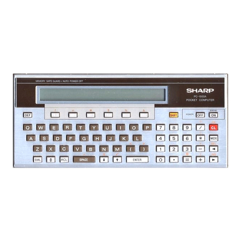
Sharp PC-1500A User manual

Sharp
Sharp MZ-800 User manual

Sharp
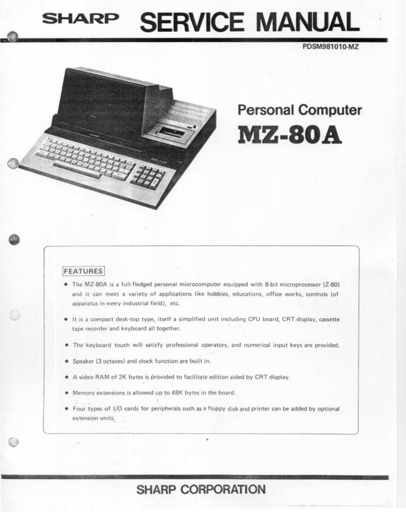
Sharp MZ-80A User manual