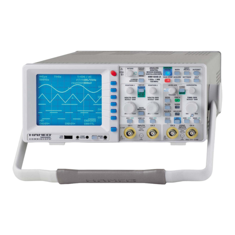
Hameg CombiScope HM1508-2 User manual

Release: April, 2008
150 MHz
Mixed Signal CombiScope®
HM1508-2
Servicemanual
English

2Subject to change without notice
General information regarding the CE marking
HAMEG instruments fulfill the regulations of the EMC directive. The
conformity test made by HAMEG is based on the actual generic- and
product standards. In cases where different limit values are applicable,
HAMEG applies the severer standard. For emission the limits for
residential, commercial and light industry are applied. Regarding the
immunity (susceptibility) the limits for industrial environment have
been used.
The measuring- and data lines of the instrument have much influence
on emission and immunity and therefore on meeting the acceptance
limits. For different applications the lines and/or cables used may
be different. For measurement operation the following hints and
conditions regarding emission and immunity should be observed:
1. Data cables
For the connection between instrument interfaces and external devices,
(computer, printer etc.) sufficiently screened cables must be used.
Without a special instruction in the manual for a reduced cable length,
the maximum cable length of a dataline must be less than 3 meters and
not be used outside buildings. If an interface has several connectors
only one connector must have a connection to a cable.
Basically interconnections must have a double screening. For IEEE-bus
purposes the double screened cables HZ73 and HZ72L from HAMEG
are suitable.
2. Signal cables
Basically test leads for signal interconnection between test point and
instrument should be as short as possible. Without instruction in the
manual for a shorter length, signal lines must be less than 3 meters
and not be used outside buildings.
Signal lines must screened (coaxial cable - RG58/U). A proper ground
connection is required. In combination with signal generators double
screened cables (RG223/U, RG214/U) must be used.
3. Influence on measuring instruments
Under the presence of strong high frequency electric or magnetic
fields, even with careful setup of the measuring equipment, influence
of such signals is unavoidable.
Die HAMEG Instruments GmbH bescheinigt die Konformität für das Produkt
The HAMEG Instruments GmbH herewith declares conformity of the product
HAMEG Instruments GmbH déclare la conformite du produit
Bezeichnung / Product name / Designation:
Oszilloskop
Oscilloscope
Oscilloscope
Typ / Type / Type: HM1508-2
mit / with / avec: HO720
Optionen / Options / Options: HO730, HO740
mit den folgenden Bestimmungen / with applicable regulations / avec les
directives suivantes
EMV Richtlinie 89/336/EWG ergänzt durch 91/263/EWG, 92/31/EWG
EMC Directive 89/336/EEC amended by 91/263/EWG, 92/31/EEC
Directive EMC 89/336/CEE amendée par 91/263/EWG, 92/31/CEE
Niederspannungsrichtlinie 73/23/EWG ergänzt durch 93/68/EWG
Low-Voltage Equipment Directive 73/23/EEC amended by 93/68/EEC
Directive des equipements basse tension 73/23/CEE amendée par 93/68/CEE
Angewendete harmonisierte Normen / Harmonized standards applied / Normes
harmonisées utilisées:
Sicherheit / Safety / Sécurité: EN 61010-1:2001 (IEC 61010-1:2001)
Überspannungskategorie / Overvoltage category / Catégorie de surtension: II
Verschmutzungsgrad / Degree of pollution / Degré de pollution: 2
Elektromagnetische Verträglichkeit / Electromagnetic compatibility /
Compatibilité électromagnétique
EN 61326-1/A1 Störaussendung / Radiation / Emission:
Tabelle / table / tableau 4; Klasse / Class / Classe B.
Störfestigkeit / Immunity / Imunitée:Tabelle / table / tableau A1.
EN 61000-3-2/A14 Oberschwingungsströme / Harmonic current emissions /
Émissions de courant harmonique:
Klasse / Class / Classe D.
EN 61000-3-3 Spannungsschwankungen u. Flicker / Voltage fluctuations and flicker /
Fluctuations de tension et du flicker.
Datum /Date /Date
01. 12. 2006
Unterschrift / Signature / Signatur
Manuel Roth
Manager
This will not cause damage or put the instrument out of operation. Small
deviations of the measuring value (reading) exceeding the instruments
specifications may result from such conditions in individual cases.
4. RF immunity of oscilloscopes.
4.1 Electromagnetic RF field
The influence of electric and magnetic RF fields may become visible
(e.g. RF superimposed), if the field intensity is high. In most cases
the coupling into the oscilloscope takes place via the device under
test, mains/line supply, test leads, control cables and/or radiation.
The device under test as well as the oscilloscope may be effected by
such fields.
Although the interior of the oscilloscope is screened by the cabinet,
direct radiation can occur via the CRT gap. As the bandwidth of
each amplifier stage is higher than the total –3dB bandwidth of the
oscilloscope, the influence of RF fields of even higher frequencies
may be noticeable.
4.2 Electrical fast transients / electrostatic discharge
Electrical fast transient signals (burst) may be coupled into the
oscilloscope directly via the mains/line supply, or indirectly via test
leads and/or control cables. Due to the high trigger and input sensitivity
of the oscilloscopes, such normally high signals may effect the trigger
unit and/or may become visible on the CRT, which is unavoidable.
These effects can also be caused by direct or indirect electrostatic
discharge.
HAMEG Instruments GmbH
Hersteller HAMEG Instruments GmbH KONFORMITÄTSERKLÄRUNG
Manufacturer Industriestraße 6 DECLARATION OF CONFORMITY
Fabricant D-63533 Mainhausen DECLARATION DE CONFORMITE

3
Subject to change without notice
Contents
CombiScope HM1508-2 4
Specifications 5
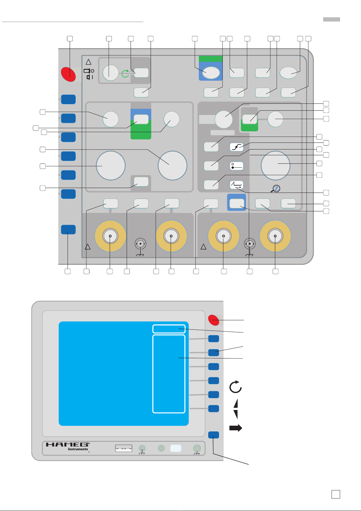
Front Panel Elements – Brief Description 7
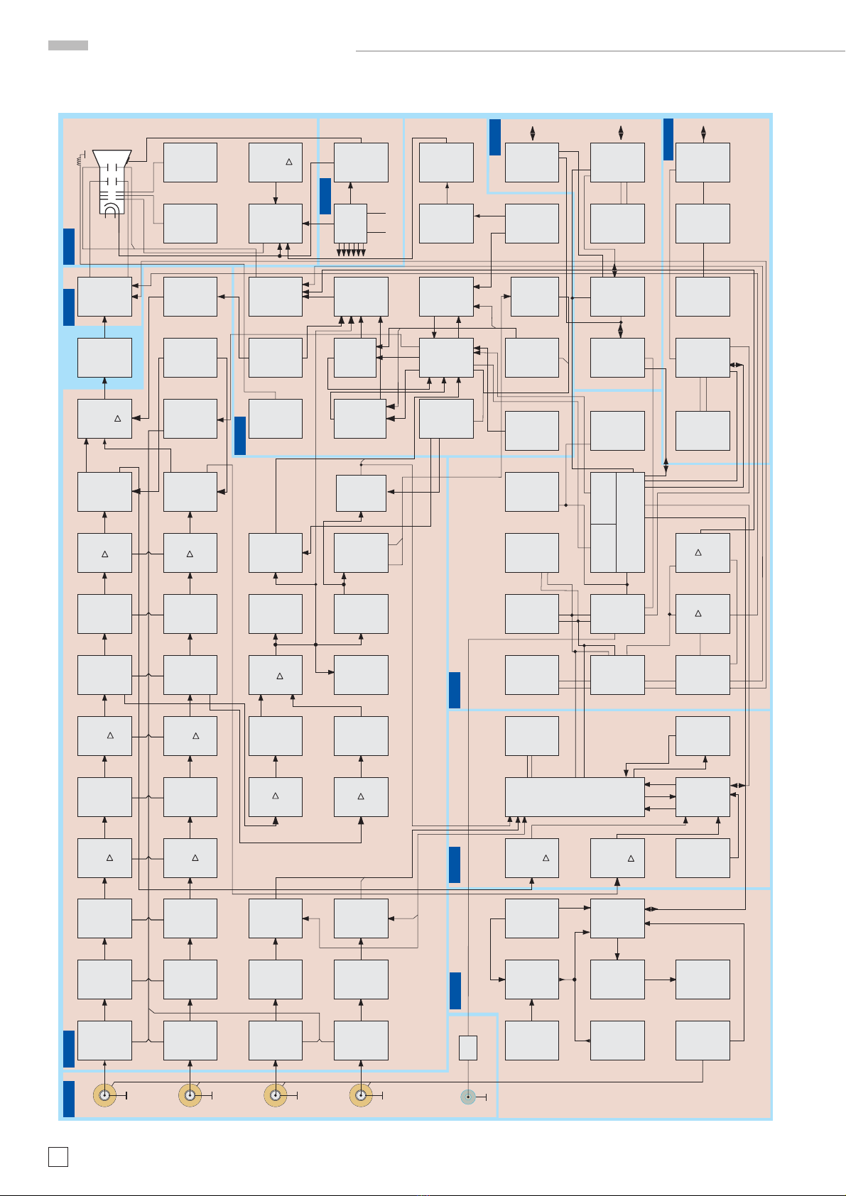
Blockdiagram 10
Short Description of HM1508-2 Boards 11
1. TE Board 11
2. YP Board 11
3. Delay Line 11
4. YF Board 12
5. MB Board 12
6. FC Board 12
7. AB Board 12
8. MC Board 12
9. IF Board 12
10.PS Board 12
11. CR Board 12
12. USB Host 12
PCB Interconnections 13
HM1508-2 Troubleshooting 16
A: Opening the Oscilloscope 16
B: Preliminary Test 17
C: Error Diagnostics 20
Performance Check HM1508-2 28
A Test Instruments required 28
B Performance Check 28
C Software Adjustment Menu 28
D Checks 29
Spare-Part List HM1508-2 36
HZ620 System description 37
Signals of HZ620 37
Selecting Signals and Sub Function 37
Calibration of the Square-wave amplitude 38
Calibrating the DC-voltage from –2V to +3V 38
Commands of the serial RS-232 interface 38
Commands for signal selection 38
Frequency selection 39
Amplitude selection 39
HM1X0X Oscilloscopes Test and Adjustment 40
1. Preliminary remark 40
2. Preparation for COM Port operation 40
3. Preparation for USB operation 40
4. PSH Adjustment Software installation 43
5. PSH operation 43
Adjustment Procedure 50

4Subject to change without notice
HM1508-2
1 GSa/s Real Time Sampling, 10 GSa/s Random Sampling
1 MPts Memory per Channel, Memory oom up to 50,000:1
FFT for spectral analysis
4 Channels (2 analog, 2 logic inputs)
Deflection coefficients: 1 mV/cm – 20 V/cm,
Time Base: 50 s/cm – 5 ns/cm
8-Bit Low Noise Flash A/D Converters
Acquisition modes: Single, Refresh, Average, Envelope,
Roll, Peak-Detect
Front USB-Stick Connector for Screenshots
USB/RS-232 Interface
optional: IEEE-488, Ethernet/USB Interface
Signal display: Yt, XY and FFT;
Interpolation: Sinx/x, Pulse, Dot Join (linear)
Analog mode: see HM1500-2
DSO mode: Signal portion
expanded with zoom (color
burst in one line of a
composite video signal)
Frequency Analysis
with FFT
DSO mode:
4-channel display of 2
analog and 2 logic signals
150 MHz Mixed Signal CombiScope®
with FFT HM1508-2

5
Subject to change without notice
150 MHz Mixed Signal CombiScope®HM1508-2
Valid at 23 °C after a 30 minute warm-up period
Vertical Deflection
Channels:
Analog: 2
Digital: 2 + 2 Logic Channels
Operating Modes:
Analog: CH 1 or CH 2 separate, DUAL (CH 1 and
CH 2 alternate or chopped), Addition
Digital: Analog Signal Channels CH 1 or CH 2
separate, DUAL (CH 1 and CH 2), Addition
Logic Signal Channels: CH 3 and CH 4
X in XY-Mode: CH 1
Invert: CH 1, CH 2
Bandwidth (-3 dB): 2 x 0 – 150MHz
Rise time: ‹ 2.3 ns
Overshoot: max. 1 %
Bandwith limiting (selectable):about 20 MHz (5 mV/cm - 20 V/cm)
Deflection Coefficients(CH 1,2):14 calibrated steps
1mV – 2 mV/cm (10MHz) ± 5 % (0 – 10 MHz (-3 dB))
5 mV – 20 V/cm ± 3 % (1-2-5 sequence)
variable (uncalibrated): › 2.5 :1 to › 50 V/cm
Inputs CH 1, 2:
Input Impedance: 1 MΩ II 15 pF
Coupling: DC, AC, GND (ground)
Max. Input Voltage: 400 V (DC + peak AC)
Y Delay Line (analog): 70 ns
Measuring Circuits: Measuring Category I
Digital mode only:
Logic Channels: CH 3, CH 4
Select. switching thresholds: TTL, CMOS, ECL
User definable thresholds: 3
within the range: -2 V to +3 V
Analog mode only:
Auxiliary input: CH 4: 100 V (DC + peak AC)
Function (selectable): Extern Trigger, Z (unblank)
Coupling: AC, DC
Max. input voltage: 100 V (DC + peak AC)
Triggering
Analog and Digital Mode
Automatic (Peak to Peak):
Min. signal height: 5mm
Frequency range: 10 Hz - 250 MHz
Level control range: from Peak- to Peak+
Normal (without peak):
Min. signal height: 5mm
Frequency range: 0 - 250 MHz
Level control range: –10 cm to +10 cm
Operating modes: Slope/Video/Logic
Slope: positive, negative, both
Sources: CH 1, CH 2, alt. CH 1/2 (≥8 mm, analog
mode only), Line, Ext.
Coupling: AC: 10 Hz-250 MHz
DC: 0-250 MHz
HF: 30 kHz–250 MHz
LF: 0-5kHz
Noise Rej. switchable
Video: pos./neg. Sync. Impulse
Standards: 525 Line/60 Hz Systems
625 Line/50 Hz Systems
Field: even/odd/both
Line: all/line number selectable
Source: CH 1, CH 2, Ext.
Indicator for trigger action: LED
External Trigger via: CH 4 (0.3 Vpp, 150 MHz)
Coupling: AC, DC
Max. input voltage: 100 V (DC +peak AC)
Digital mode:
Logic: AND/OR, TRUE/FALSE
Source: CH1 or 2, CH3 and CH4
State: X, H, L
Pre/Post Trigger: -100 % to +400% related to complete memory
Analog mode
2nd Trigger
Min. signal height: 5mm
Frequency range: 0 - 250 MHz
Coupling: DC
Level control range: –10 cm to +10 cm
Horizontal Deflection
Analog mode
Operating modes: A, ALT (alternating A/B), B
Time base A: 0.5 s/cm - 50 ns/cm (1-2-5 sequence)
Time base B: 20 ms/cm – 50 ns/cm (1-2-5 sequence)
Accuracy A and B: ±3%
X Magnification x10: to 5 ns/cm
Accuracy: ±5%
Variable time base A/B: cont. 1:2.5
Hold Off time: var. 1:10 LED-Indication
Bandwidth X-Amplifier: 0 - 3 MHz (-3 dB)
X Y phase shift ‹ 3°: ‹ 220 kHz
Digital mode
Time base range (1-2-5 sequence)
Refresh Mode: 20 ms/cm - 5 ns/cm
with Peak Detect: 20ms/cm – 2ms/cm (min. Pulse Width 10 ns)
Roll Mode: 50 s/cm – 50 ms/cm
Accuracy time base
Time base: 50 ppm
Display: ±1%
MEMORY ZOOM: max. 50,000:1
Bandwidth X-Amplifier: 0 - 150 MHz (-3 dB)
XY phase shift ‹ 3°: ‹ 100 MHz
Digital Storage
Sampling rate (real time): Analog channels: 2 x 500 MSa/s, 1 GSa/s
interleaved; Logic Channels: 2 x 500 MSa/s
Acquisition (random sampling): 10GSa/s
Bandwidth: 2 x 0 - 150 MHz (random)
Memory: 1 M-Samples per channel
Operating modes: Refresh, Average, Envelope/
Roll: Free Run/Triggered, Peak-Detect
Resolution (vertical): 8 Bit (25 Pts/cm)
Resolution (horizontal):
Yt: 11 Bit (200 Pts/cm)
XY: 8 Bit (25 Pts /cm)
Interpolation: Sinx/x, Dot Join (linear), Pulse
Delay: 1 Million x 1/Sampling Rate to
4 Million x 1/Sampling Rate
Display refresh rate: max.170/s at 1 MPts
Display: Dots (acquired points only), Vectors (partly
interpolated), optimal (complete memory
weighting and vectors)
Reference Memories: 9 with 2 kPts each (for recorded signals)
Display: 2 signals of 9 (free selectable)
FFT Mode
Display X: Frequency Range
Disaplay Y: True rms value of spectrum
Scaling: Linear or logarithmic
Level display: dBV, V
Window: Square, Hanning, Hamming, Blackmann
Control: Center frequency, Span
Marker: Frequency, Amplitude
Zoom (frequency axis): x10
Operation/Measuring/Interfaces
Operation: Menu (multilingual), Autoset,
help functions (multilingual)
Save/Recall (instrument parameter settings): 9
Signal display: max. 4 signals or 4 traces
analog: CH 1, 2 (Time Base A) in combination with
CH 1, 2 (Time Base B)
digital: CH 1, 2 and CH 3, 4 or ZOOM or Reference
or Mathematics
USB Memory-Stick:
Save/Recall external:
Instrument settings and Signals: CH 1, 2 and CH 3, 4 or ZOOM or
Reference or Mathematics
HM1508-2 Specifications

6Subject to change without notice
Screen-shot: as Bitmap
Signal display data (2k per channel): Binary (SCPI-Data), Text (ASCII-
Format), CSV (Spread Sheet)
Frequency counter:
6 digit resolution: › 1 MHz – 250 MHz
5 digit resolution: 0.5 Hz – 1 MHz
Accuracy: 50 ppm
Auto Measurements:
Analog mode: Frequency, Period, Vdc, Vpp, Vp+, Vp-
also in digital mode: Vrms, Vavg
Cursor Measurements:
Analog mode: Δt, 1/Δt (f), tr, ΔV, V to GND, ratio X, ratio Y
plus in digital mode: Vpp, Vp+, Vp-, Vavg, Vrms, pulse count
Resolution Readout/Cursor: 1000 x 2000 Pts, Signals: 250 x 2000
Interfaces (plug-in): USB/RS-232 (HO720)
Optional: IEEE-488, Ethernet/USB
Mathematic functions
Number of Formula Sets: 5 with 5 formulas each
Sources: CH 1, CH 2, Math 1-Math 5
Targets: 5 math. memories, Math 1-5
Functions: ADD, SUB, 1/X, ABS, MUL, DIV, SQ, POS, NEG,
INV
Display: max. 2 math. memories (Math 1-5)
Display
CRT: D14-375GH
Display area (with graticule): 8 cm x 10 cm
Acceleration voltage: approx. 14 kV
General Information
Component tester
Test voltage: approx. 7 Vrms (open circuit), approx. 50Hz
Test current: max. 7 mArms (short circuit)
Reference Potential : Ground (safety earth)
Probe ADJ Output: 1 kHz/1 MHz square wave signal 0.2 Vpp (tr ‹ 4 ns)
Trace rotation: electronic
Line voltage: 105 – 253 V, 50/60 Hz ±10%, CAT II
Power consumption: 47 Watt at 230V, 50 Hz
Protective system: Safety class I (EN61010-1)
Weight: 5.6 kg
Cabinet (W x H x D): 285 x 125 x 380 mm
Ambient temperature: 0° C ...+40° C
Accessories supplied: Line cord, Operating manual, 4 Probes 10:1 with
attenuation ID (HZ200), Windows Software for control and data transfer
Optional accessories:
HO730 Dual-Interface Ethernet/USB,
HO740 Interface IEEE-488 (GPIB),
HZ70 Opto-Interface (with optical fiber cable)
HM1508-2E/260107/ce · Subject to alterations · © HAMEG Instruments GmbH · ® Registered Trademark · DQS-certified in accordance with DIN EN ISO 9001:2000, Reg.-No.: DE-071040 QM
HAMEG Instruments GmbH · Industriestr. 6 · D-63533 Mainhausen · Tel +49 (0) 6182 800 0 · Fax +49 (0) 6182 800 100 · www.hameg.com · info@hameg.com
A Rohde & Schwarz Company
www.hameg.com
Specifications

7
Subject to change without notice
1
POWER (pushbutton switch) – Turns scope on and off.
2
INTENS (knob)
Intensity for trace- and readout brightness, focus and trace
rotation control.
3
FOCUS, TRACE, MENU (pushbutton switch)
Calls the Intensity Knob menu to be displayed and enables
the change of different settings by aid of the INTENS knob.
See item 2.
4
CURSOR MEASURE (pushbutton switch)
Calls the ”Cursor” menu and offers measurement selection
and activation.
5
ANALOG/DIGITAL (pushbutton switch)
Switches between analog (green) and digital mode (blue).
6
STOP / RUN (pushbutton switch)
RUN: Signal data acquisition enabled.
STOP: Signal data acquisition is stopped
STOP (flashing): Signal data acquisition is in progress and
will be stopped after being completed.
7
MATH (pushbutton switch)
Calls mathematical function menu if digital mode is pre-
sent.
8
ACQUIRE (pushbutton switch)
Calls the signal capture and display mode menu in digital
mode.
9
SAVE/RECALL (pushbutton switch)
Offers access to the reference signal (digital mode only)
and the instrument settings memory.
10
SETTINGS (pushbutton switch)
Opens menu for language and miscellaneous function; in
digital mode also signal display mode.
11
AUTOSET (pushbutton switch)
Enables appropriate, signal related, automatic instrument
settings.
12
HELP (pushbutton switch)
Switches help texts regarding controls and menus on/off.
13
POSITION 1 (knob)
Controls position of actual present functions: Signal (current,
reference or mathematics), Cursor and ZOOM (digital).
14
POSITION 2 (knob)
Controls position of actual present functions: Signal
(current, reference or mathematics) Cursor and ZOOM
(digital).
Front Panel Elements – Brief Description
HM 1508-2 - DKL - 12/10/06 gw
HM
1508
-
2
-
TXT
gr
ü
n -
06/11/06
gw
VAR VAR VAR x10
HM 1508-2 -TXT blau - 06/11/06 gw
FFT-
Marker
POSITION 1 POSITION 2 HORIZONTAL
CH 3 CH 4
MATH
SAVE/
RECALL AUTOSET
ACQUIRE SETTINGS HELP
CH 1/2
VOLTS / DIV
SCALE
·
VAR
VOLTS / DIV
SCALE
·
VAR
TIME / DIV
SCALE
·
VAR
20V 1 mV 20V 1 mV
X-POS
INPUTS
1MΩII15pF
max
400 Vp
X-INP
LOGIC
INPUTS
1MΩII15pF
max
100 Vp
INTENS
!
TRIGGER
LEVEL A/B
HM1508-2
ANALOG
DIGITAL
MIXED SIGNAL
OSCILLOSCOPE
1 GSa ·1 MB
150 MHz
50s 5ns
CURSOR
DIGITAL
ANALOG
DELAY
CH 3/4
MA/REF
ZOOM
FOCUS
TRACE
MENU
CAT I
!
CAT I
!
MODE
FILTER
SOURCE
TRIG’d
NORM
HOLD OFF
VERT/XY
CH 3/4
CURSOR
MEASURE
FFT
RUN / STOP
CH 1 CH 2
TRIG. EXT. / Z-INP.
CH 1 CH 2 HOR MAG
AUTO
MEASURE
POWER
POWER
MENU
MENU
OFF
OFF
20
1 2 3 45 6 7 8 9 10 11 12
16
19
36
26
39
29
38
35
3431 32 33
18
15
27
23
25
21
28
24
22
30
17
14
13
37
44
Front Panel Elements – Brief Description

8Subject to change without notice
Front Panel Elements – Brief Description
15
CH1/2-CURSOR-CH3/4-MA/REF-ZOOM (pushbutton)
Calls the menu and indicates the current function of POSI-
TION 1 and 2 controls.
16
VOLTS/DIV-SCALE-VAR (knob)
Channel 1 Y deflection coefficient, Y variabel and Y scaling
setting.
17
VOLTS/DIV-SCALE-VAR (knob)
Channel 2 Y deflection coefficient, Y variabel and Y scaling
setting.
18
AUTO MEASURE (pushbutton)
Calls menus and submenus for automatic measurement.
19
LEVEL A/B - FFT-Marker (knob)
Trigger level control for A- and B Time Base. Marker position
shift in FFT mode.
20
MODE (pushbutton switch)
Calls selectable trigger modes.
21
FILTER (pushbutton switch)
Calls selectable trigger filter (coupling) and trigger slope
menu.
22
SOURCE (pushbutton) –Calls trigger source menu.
23
TRIG’d (LED)
Lit when the trigger signal meets the trigger conditions.
24
NORM (LED)
Lit if NORMAL or SINGLE event triggering is chosen.
25
HOLD OFF (LED)
Lit if a hold off time is set (only in analog mode) >0% in the
HOR menu (HOR VAR pushbutton
30
).
26
X-POS / DELAY (pushbutton)
Calls and indicates the actual function of the HORIZONTAL
knob
27
, (X-POS dark).
27
HORIZONTAL (knob)
Changes the X position or in digital mode, the delay time
(Pre- or Post-Trigger). In FFT mode for center frequency
control.
28
TIME/DIV-SCALE-VAR (knob)
Setting of A and B time base (deflection coefficient), time
fine control (VAR; only in analog mode) and scaling; Span
in FFT mode.
29
MAG x10 (pushbutton)
10 fold expansion in X direction in Yt mode, with simulta-
neous change of the deflection coefficient display in the
readout.
30
HOR / VAR (pushbutton)
Calls ZOOM function (digital) and analog time base A and
B, time base variable and hold off control.
31
CH1 / VAR (pushbutton)
Calls channel 1 menu with input coupling, inverting, probe
and Y variable control.
32
VERT/XY (pushbutton)
Calls ver tical mode selection, addition, XY mode and band-
width limiter.
33
CH2 / VAR (pushbutton)
Calls channel 1 menu with input coupling, inverting, probe
and Y variable control.
34
Input CH1 (BNC socket)
Channel 1 signal input and input for horizontal deflection
in XY mode.
35
Input CH2 (BNC socket) – Channel 2 signal input.
36
CH3/4 (pushbutton)
Digital mode: Logic signal channels 3 and 4. On condition
OFF, CH4 becomes the external trigger input.
Analog mode: CH4 can be used for intensity modulation (Z)
if external triggering is switched off.
37
FFT (pushbutton)
Calls FFT menu, offers window and scaling selection, as
well as function switch off. Calls FFT menu if FFT mode
is present. Direct switch over from digital Yt mode to FFT
mode.
38
CH3 LOGIC INPUT (BNC socket)
Input for logic signals in digital mode.
39
CH4 LOGIC INPUT (BNC-socket)
Digital mode: Input for logic signals or external trigger
signals. Analog mode: Input for intensity modulation (Z) or
external trigger signals.
40
PROBE / ADJ (socket)
Square wave signal output for frequency compensation of
x10 probes.
41
PROBE / COMPONENT (pushbutton)
Calls menu that offers COMPONENT Tester operation,
frequency selection of PROBE ADJ square wave signal,
hardware and software information and details about in-
terface (rear side) and USB Stick (flash drive) connector.
42
COMPONENT TESTER (2 sockets with 4 mm Ø)
Connectors for test leads of the Component Tester. Left
socket is galvanically connected with protective earth.
43
USB Stick (USB flash drive connector)
Enables storage and load of signals and signal parameters
in connection with USB flash drives.
44
MENU OFF (pushbutton)
Switches the menu display off or one step back in the menu
hierarchy.
HM 1
5
HM 1
5
COMBISCOPE
USB
Stick
COMP.
TESTER
PROBE
ADJ
POWER
MENU
OFF
4440414243

9
Subject to change without notice
Front Panel Elements – Brief Description
HM 1508-2 - DKL - 12/10/06 gw
HM
1508
-
2
-
TXT
gr
ü
n -
06/11/06
gw
VAR VAR VAR x10
HM 1508-2 -TXT blau - 06/11/06 gw
FFT-
Marker
POSITION 1 POSITION 2 HORIZONTAL
CH 3 CH 4
MATH
SAVE/
RECALL AUTOSET
ACQUIRE SETTINGS HELP
CH 1/2
VOLTS / DIV
SCALE ·VAR
VOLTS / DIV
SCALE ·VAR
TIME / DIV
SCALE ·VAR
20V 1 mV 20V 1 mV
X-POS
INPUTS
1MΩII15pF
max
400 Vp
X-INP
LOGIC
INPUTS
1MΩII15pF
max
100 Vp
INTENS
!
TRIGGER
LEVEL A/B
HM1508-2
ANALOG
DIGITAL
MIXED SIGNAL
OSCILLOSCOPE
1 GSa
·
1 MB
150 MHz
50s 5ns
CURSOR
DIGITAL
ANALOG
DELAY
CH 3/4
MA/REF
ZOOM
FOCUS
TRACE
MENU
CAT I
!
CAT I
!
MODE
FILTER
SOURCE
TRIG’d
NORM
HOLD OFF
VERT/XY
CH 3/4
CURSOR
MEASURE
FFT
RUN / STOP
CH 1 CH 2
TRIG. EXT. / Z-INP.
CH 1 CH 2 HOR MAG
AUTO
MEASURE
POWER
POWER
MENU
MENU
OFF
OFF
HM2008 - HINT - Stand: 10/10/06 gw
HM2008 - DKL - Stand: 10/10/06 gw
HM2008 - TXT blau - Stand: 06/11/06 gw
HM 2008 - TXT grün - Stand: 06/11/06 gw
HM2008 - TXT SW - Stand: 06/11/06 gw
COMBISCOPE
USB
Stick
COMP.
TESTER
PROBE
ADJ
CH I MENU
AC/DC/50 Ω
GND
50 Ω/ 1 MΩ
INVERT
ON / OFF
VARIABLE
ON / OFF
PROBE
1 : 1 / 10 / 100
CH I: 500 mV
POWER
POWER
MENU
MENU
OFF
OFF
Pushbutton
Menu Title
6 Function Pushbuttons (blue)
Menu
Intensity Knop Symbol
Arrow Keys
Indicator for Submenu
State indication by intensified display
MENU OFF (pushbutton)
On Off
44 31 34 32 33 35 36 38 37 39
13
15 14
17
16
18
19
26
27
20
23
21
24
28
22
25
29
30
121110
987654321

10 Subject to change without notice
Blockdiagram HM1508-2
FC Board AB Board MC Board
MB Board
CR Board
PS Board
YF BoardYP Board
TE Board
IF Board
USB Host
PROBE
ADJ
CH 1
CH 2
CH 3
CH 4
Impedance
Converter
(FET)
Buffer
Pre-
Amplifier
*1 / *5
Attenuator
4 : 1
2 : 1
1 : 1
Comparator
Attenuator
100 : 1
10 : 1
1 : 1
Impedance
Converter
ComparatorImpedance
Converter
Input
Coupling
AC / DC
Input
Coupling
AC / DC
Var.
Gain
Intermediate
Trigger
CH1
Amplifier
Intermediate
Trigger
CH2
Amplifier
Symmetry
&
Trigger
Pick Off
Trigger
Channel
Switch
Trigger
Channel
Switch
Inverting
Switch
Trigger
Amplifier
Intermediate
Amplifier
Y-Pos
Control
LF
Filters
Channel
Switch
& Digital
Pick Off
Impedance
Converter
(FET)
Buffer
Pre-
Amplifier
*1 / *2
Attenuator
4 : 1
2 : 1
1 : 1
Attenuator
100 : 1
10 : 1
1 : 1
Input
Coupling
AC / DC
Var.
Gain
Symetrie
&
Trigger
Pick Off
Inverting
Switch
Intermediate
Amplifier
Y-Pos
Control
Channel
Switch
& Digital
Pick Off
TB B
Trigger
Comparator
TB A
Trigger
Comparator
Delay
Line
Driver
Y
Control
Delay
Line
Trace
Rotation
Buffer
Amplifier
Channel
Switch
Driver &
CT Switch
CT
Generator
CT
Y Coupling
Switch
Y Final Ampl.
Digital &
Readout
Inp.
X Final Ampl.
Mag x10
Dig &
Readout
Input &
Control
Focus
Control
Blanking
Switch
&
Amplifier
Astigmatism
Adjust
Blanking
Final
Amplifier
Input
Coupling
AC / DC
TV Sync.
Separator
& Slope
Selection
Trigger
Coupling
&
Line Input
Trigger
PP
Circuit
Shift &
Store
Bus
Register
Shift &
Store
Bus
Register
Analog
Switch
Rotary
Pulse
Encoder
CAL
ProcessorKeyboard
Frontpanel
LEDs
Analog
Multi-/
Demulti-
plexer
CH 1
Buffer
Amplifier
CH 2
Buffer
Amplifier
PLL
Frequency
Synthesizer
A / D
Converter
1 GSa/s
Control
Unit
FPGA
Static
RAM
Readout
RAM
Flash
RAM
SDRAM Delay
Comparator
Readout
FPGA
RISC
CPU
PLD
Time
Measuring
Readout
D AC
S & H
Integrate
S & H
Integrate
Sweep B
Generator
& Control
Sweep A
Generator
& Control
Input
Control
Sweep A,B
CT-X, XY
Power
Supply
Line / Mains
HV
Generator
& Voltage
Multiplier
10 bit
D / A
Converter
Time Base
Control
PLD
Shift / Store
Register
10 Bit
A / D
Converter
F
RAM
8k x 8bit
Serial
Flash
RAM
Hold
Off
Analog
Multiplier
Blanking
Driver
8bit
D / A
Converter
RS-232
Receiver
EEPROM
/8
/16
/3
/8/4
/2
/4
/2
/2/2
/2/2
/2/2/2/2
/2/2/2/2
/4
/4/2
/4
CPU - ADDR
CPU - DATA
/2
/2
/2
/2
/2
/6
/14
/2
/2
/2/28x
8Bit
/2
/2
/2
/4
SRAM
Switch CPU USB
Receiver
CPU USB
Power
Over-
current
Protection
USB
Connector
Trigger
Counter
SPI
Switch
/4

11
Subject to change without notice
Short Description of HM1508-2 Boards
Preliminary note:
This short description refers to the HM1508 block diagram. It
contains the most important functions, but not all.
1. TE Board
1.1 Probe identification
The contact area around the BNC sockets (CH1 to CH4) is for
probe identification contact recognition. The information from
the probe’s internal identification resistor is input in the proces-
sor system and automatically changes parameters regarding
the probe’s divider ratio.
1.2 CALibrator Signal
The calibrator signal originates from the MC board, controls
the driver and is available at the PROBE ADJ socket.
2. YP Board
2.1 CH1 and CH2
The measuring signal at the input is connected through a swit-
chable high impedance attenuator, galvanically (DC coupled) or
via an input capacitor (AC coupled) to the input FET (impedance
converter). The following measuring amplifier stages are DC
coupled.
The next stage is the Pre Amplifier, where for 1 mV/cm and
2 mV/cm ranges, an additional amplification by 5 is made.
The following low impedance attenuator allows the selection of all
Y deflection coefficients from 1 mV/cm to 20 V/cm, in connection
with the high impedance attenuator and the Pre Amplifier.
The fixed Y deflection coefficient can also be set to uncali-
brated intermediate values in the VAR Gain stage. Additio-
nally the signal is converted from an asymmetric signal into
2 symmetrical signals with a phase difference of 180°. The
following stages up to the Delay Line Driver are designed as
two identical amplifiers.
The Symmetry and Trigger Pick Off stage is used to correct
asymmetries and thereafter the selection of the measurement
signal to be used for internal triggering.
If activated, the Inverting Switch reverses the 2 (180° different)
measuring signals to be amplified in the following stages. The
result is a 180° turned (inverted) signal display.
In the Intermediate Amplifier the DC current of both identical
amplifiers is controlled in such a way, that if the current in one
amplifier is reduced it increases in the other amplifier by the
same amount. This causes a trace position shift in (Y position).
Thereafter the measuring signals of CH1 and CH2 are input in
the Channel Switch & Digital Pick Off stage. Before entering
the channel switch, the CH1 and CH2 measuring signals are
picked off and feed the channel 1 and 2 buffer amplifiers on
AB board. The channel switch is active in analogue mode and
selects which signal is output and feeds the Delay Line Driver.
The channel switch is controlled by the Channel Switch, Driver
& CT Switch stage.
The Delay Line stage converts the signal to the wave resistance
stage of the delay line.
2.2 CH3 and CH4 (only digital)
The measuring signal at the input is connected to an FET (im-
pedance converter) galvanically (DC coupling) or via an input
capacitor (AC coupling).
In the following Comparator stages the state of the digital logic
input signals are compared with logic threshold voltages. The
comparison result of each comparator is connected to the
Control Unit FPGA on AB board.
2.3 Trigger Section
The CH1 and CH2 measuring signals originating from the
measuring amplifier Trigger Pick Off are amplified in the In-
termediate Trigger Amplifier CH1 and CH2.
These signals later used for internal triggering are input in
the Trigger Channel Switch stage, which is active in analogue
and digital mode. The signal to be used for internal triggering
is selected by the switch.
This signal enters the Trigger Amplifier stage for additional
amplification.
The output signal is connected with the LF Filter, TV Sync. Se-
parator & Slope Selection and Trigger Coupling & Line Input
stage. The selected stage serves as the source for the TB A
(time base A) Trigger Comparator and the Trigger PP (peak to
peak) Circuit.
The Trigger Amplifier output signal is also the DC coupled
source of the TB B Trigger Comparator (time base B) which
can be used in analog mode only.
The Trigger PP Circuit generates a signal height dependent
voltage that can be used for trigger level setting at the time
base A trigger comparator.
Both time base A and B reference voltages are generated by
the 10 bit D/A Converter on MB board.
The time base A and B trigger comparator output signals are
connected with the Time Base Control PLD on MB board for
analog time base triggering. Additionally the time base A trigger
comparator output signal is also connected with the Control
Unit FPGA on AB board for digital time base triggering.
2.4 Y Control
This stage encodes all control functions for attenuator, variable,
position, inverting and other Y amplifier related functions.
2.5 Channel Switch, Driver and CT Switch
This stage encodes all control functions regarding the channel
switches, switches in the driver section and the component
tester (CT) switch over.
2.6 CT Y Coupling Switch
Switches the analogue measuring signal off in the Delay Line
Driver stage and inputs the vertical component of the compo-
nent tester (CT) signal.
3. Delay Line
3.1 The delay line introduces a delay of the analogue measu-
ring signal, so that switching and other delays in the trigger
Short Description of HM1508-2 Boards

12 Subject to change without notice
and time base section are compensated and the trigger slope
becomes visible.
4. YF Board
4.1 The analogue measuring signal is amplified and controls
the Y plates of the cathode ray tube (CRT).
4.2 In digital mode the Y signal and the Y component of the read-
out are input here for Y deflection. Both signals originate from
data in the Readout FPGA (MC board) which has been converted
by the Readout DAC (MC board) into analogue signals. Whether
the data are displayed as dots or vectors depends on the activa-
tion of the S&H (MC board) circuit in the signal path.
5. MB Board
The main function is to generate sweep (sawtooth) signals in
analog mode for time base A and B in the Sweep A Generator &
Control stage and the Sweep B Generator & Control stage.
The sweep start of both analog time bases is controlled by the
Time Base Control PLD in connection with the Hold Off stage
and the trigger signals coming from the time base A and B
trigger comparators located on YP board.
The sweep deflection time (coefficient) depends on the Shift
/ Store Register data controlling both sweep generators and
the Hold Off stage.
The Delay Comparator controls the time base B delay time,
comparing the A sweep height with a reference voltage.
The Input Control: Sweep A, B, CT-X and XY stage selects between
time base sweep A and B, the X deflection component of the
component tester (CT) and the signal to be used for X deflection
in XY mode.
The signals mentioned above are analog mode signals and
output to the X Final Amplifier, Mag x10, Dig. & Readout Input
& Control stage. Additionally this stage accepts the X deflec-
tion signal and the X deflection component of the readout in
analogue and digital mode. Both signals originate from data
in the Readout FPGA (MC board) which has been converted by
the Readout DAC (MC board) into analogue signals. The fol-
lowing S&H (MC board) circuit can be used depending on dots
or vector display. The X final amplifier controls the X plates of
the cathode ray tube (CRT).
The unblank and intensity information comes from the time
base control. It is converted to analogue via an 8 bit D/A Con-
verter and controls the Blanking Switch & Amplifier (CR board)
via an Analog Multiplexer and the Blanking Driver stage.
The CT generator generates the X and Y signal components of
the component tester (CT).
The Trace Rotation Buffer Amplifier provides the trace rotation
coil on the cathode ray tube (CRT) with a current for the com-
pensation of CRT production tolerances as well as the influence
of external magnetic fields on the sweep.
6. FC Board
This board enables the user to control the instrument via key-
board and rotary pulse encoders. Probes with identifications
contacts are recognised and their probe factor is taken into
account. Additionally the user gets information about the ins-
truments state via front panel LEDs and readout information
by aid of the Readout FPGA (MC board).
7. AB Board
The AB board is used for data acquisition. The measuring si-
gnal originating from the YP board is amplified by both Buffer
Amplifiers and then input at the A/D Converter. The sampling
rate depends on the PLL Frequency Synthesizer from where
the sampling clock signal originates.
The Control Unit FPGA controls the sampling process and
saves the sampling results into a Static RAM. A Time Measu-
ring circuit is additionally used In combination with random
sampling.
After recording, the data are transferred from the Static RAM
to the memories on the MC board.
8. MC Board
The main function of this board is to store and process signal
data captured and recorded by the AB board stages. These data
and the readout data (Readout RAM) are output, converted to
analogue signals and finally after controlling the X and Y final
amplifiers, are displayed by the cathode ray tube (CRT).
The control function for these processes originates from the
PLD stage and control the affected stages via the SPI-Con-
trol-Bus.
Signal and parameter data can also be sent via the Interface
(IFboard) to external devices. It is also possible to receive data
for instrument control, firmware update etc.
9. IF Board
This board enables different interface to be input such as
RS-232, USB, Ethernet and GPIB (IEEE-488) for bi-directional
data transfer.
10.PS Board
This board contains a switch mode power supply with different
supply voltages for the instrument. It also contains –2 kV high
voltage generator, the voltage multiplier for 12 kV generation
and the heater voltage. All voltages are required for cathode
ray tube (CRT) operation.
11. CR Board
The CR board contains the Blanking Final Amplifier, the Blan-
king Switch & Amplifier, the Focus Control and the Astigmatism
Adjust. stage.
12. USB Host
The USB Host Board contains the control for the USB Memory
Stick Connector.
Short Description of HM1508-2 Boards

13
Subject to change without notice
PCB Interconnections
/50
CT
YP-Board
YF-Board
CR-Board
PS-Board
AB-Board MB-Board
FC-Board
MC-Board
TE-Board
Trace
Rotation
USB Host
IF-Board
Delay
Line
HM1508-2 - CombiScope
Interconnections (MC-F00 V2.1)
J4000
J2400J2602
W9000W9001
W6003
W6004
W6001
W6002
J1002
J1003
J1008J3
J1005
X1
J3 J4
J1
J4800 J5003
W4400
J5002 J5000
J3602
J4801 J4802
J4
J8
J5
J6 J4
J9
wire
J7000
J2
/16
/20
/8
/4
/4
/6
/6
/2
/34
/8
/8
/16
/3
/1
/1
/3
/1
/10
(+5V IF)
J3
W1
/20
PCB Interconnections

14 Subject to change without notice
Interconnections between:
YP-Board (J2400) and MB-Board (J5000)
Direction Pin Name
<-- 1 SYS-REF
<-- 2 Y2-POS
<-- 3 Y1-POS
--> 4 Board identification
<-- 5 SDO_YP
<-- 6 SCLK_YP
<-- 7 CS_YP
<-- 8 +5V
<-- 9 CT_Y
<-- 10 ALT-TB
11 -6V
<-- 12 Y2-TRG
<-- 13 Y1-TRG
14 +12V
<-- 15 Y1
<-- 16 Y2
17 VOUT_TRG
<-- 18 AUX1-LEV
--> 19 PP-
--> 20 PP+
<-- 21 TRB-LEV
<-- 22 TRA-LEV
--> 23 TRGMP
--> 24 X/Y
<-- 25 LINE-TR
--> 26 TV-LINE
<-- 27 PP-DIS
28 Reference Potential
--> 29
TRB
--> 30 TRB
--> 31
TRA
--> 32 TRA
33 Reference Potential
--> 34 Z
YP-Board (J2602) and AB-Board (J3)
Direction Pin Name
1 +12V
--> 2
D2-PO
--> 3 D2-PO
--> 4
DIG1
5 Reference Potential
--> 6
D1-PO
7 D1-PO
--> 8 -6V
YP-Board (J4000) and AB-Board (J4)
Direction Pin Name
--> 1
DIGBITA
--> 2 DIGBITA
3 Reference Potential
--> 4 DIGBITB
--> 5
DIGBITB
--> 6 DIG2
--> 7 TRA _ DG
--> 8 TRA_DG
MB-Board (J4801) and YF-Board (W9000)
Direction Pin Name
--> 1 DIG/ANA
--> 2 CT_ON
--> 3 RO_Y_POS
--> 4 RO_Y
5 +5V
6 +12V
MB-Board (J4802) and YF-Board (W9001)
Direction Pin Name
1 -6V
<-- 2 Y-DV2
<-- 3 Y-DV1
<-- 4 YF-Code
5 Reference Potential
--> 6 YDV
MB-Board (J4800) and CR-Board (W6001)
Direction Pin Name
--> 1 no name (X plate 1, CRT)
2 nc
<-- 3 YDV
<-- 4 XDV
5 nc
--> 6 no name (X plate 2, CRT)
MB-Board (J5003) and CR-Board (W6002)
Direction Pin Name
--> 1 +12V
--> 2 BLANK
3 Reference Potential
--> 4 -6V
PS-Board (J1002) and MB-Board (W4400)
Direction Pin Name
--> 1 +117V
--> 2 +65V
3 Reference Potential
--> 4 +5.2V
--> 5 LINE_TR
--> 6 +12V
--> 7 CT_V
--> 8 -6V
MB-Board (J3602) and CT/TR
Direction Pin Name
<-- 1 Comp. Tester Socket
2 nc
3 nc
4 nc
--> 5 Trace Rotation
6 Trace Rotation
(Reference Potential)
MB-Board (J5002) and MC-Board (J4)
Direction Pin Name
<-- 1 +3.3V
<-- 2 TRGCNTG
--> 3
TRIGGER
--> 4 TRG/X
--> 5 VCC_CALI
<-- 6 +2.5V
<-- 7 RO_Y
<-- 8 RO_Y_POS
--> 9 TRIG_MB
<-- 10 RO_X
<-- 11 RO_X_POS
--> 12 RO_WAIT
<-- 13 DIG/ANA
<-- 14 RO_DARK
<-- 15 D_INT_B
<-- 16 ANA_INT
--> 17 SDI_MB
<-- 18 SCLK_MB
<-- 19 SDO_MB
<-- 20 CS_MB
MC-Board (J8) and FC-Board (J4)
Direction Pin Name
--> 1 VCC_CALI
--> 2 SW_OUT
3 +5V_PS
--> 4 +3.3V
5 Reference Potential
--> 6 DEB_KEY
--> 7
CP0U _ RES
<-- 8 DRQ _ KEY
<-- 9 SDL_KEY
<-- 10 SCLK_KEY
--> 11
CPU _ CS _ SPI _ KEY
--> 12 SDD_KEY
13 nc
14 nc
15 nc
16 nc
MC-Board (J9) and USB Host (J3)
Direction Pin Name
--> +5V_IF
--> +5V_IF
GND
--> SCLK_IF1
GND
--> CS_IF1
GND
<-- SDI_IF1
GND
--> SDO_IF1
GND
<-- EXT_IF1_RES
GND
<-- EXT_IF1_ID
--> +3,3V
--> EXT_IF1_RESET_PLD
PCB Interconnections

15
Subject to change without notice
MC-Board (J5) and AB-Board (J1)
Direction Pin Name
1 Reference Potential
<-- 2 THERMO
3 nc
4 +1.5V
5 +2.5V
6 +3.3V
7 +5V_PS
--> 8 SYS_CLK
9 Reference Potential
10 CPU_DATA0
11 CPU_DATA1
12 CPU_DATA2
13 CPU_DATA3
14 CPU_DATA4
15 CPU_DATA5
16 CPU_DATA6
17 CPU_DATA7
18 CPU_DATA8
19 CPU_DATA9
20 CPU_DATA10
21 CPU_DATA11
22 CPU_DATA12
23 CPU_DATA13
24 CPU_DATA14
25 CPU_DATA15
26 Reference Potential
--> 27 TRIG_MB
28 Reference Potential
--> 29 CPU_ADDR0
--> 30 CPU_ADDR1
--> 31 CPU_ADDR2
32 Reference Potential
--> 33
CPU _ READY _ RES
--> 34 CPU _ RD
--> 35 CPU_DMQL/WE0
--> 36 CPU _ CS _ ACQ
<-- 37 DREQ _ ACQ
--> 38 DACK _ ACQ
39 Reference Potential
--> 40 LOAD_SPI_ACQ0
--> 41
CS _ SPI _ ACQ1
--> 42 SCLK_ACQ
<-- 43 SDI_ACQ
--> 44 SD0_ACQ
--> 45
ACQ _ CONF _ CS
--> 46 ACQ _ CONF _ CONFIG
<-- 47 ACQ_CONF_DONE
<-- 48
ACQ _ CONF _ STATUS
--> 49 CONF_DATA0
--> 50 CONF_DCLK
MC-Board (J6) and IF-Board (J8500)
Direction Pin Name
--> 1 +5V
2 Reference Potential
--> 3 RTS
<-- 4 CTS
5 Reference Potential
<-- 6 RxD
7 Reference Potential
--> 8 TxD
9 Reference Potential
<-- 10
EXT _ IF _ EN
11 Reference Potential
12 nc
<-- 13 EXT_IF_ID0
<-- 14 EXT_IF_ID1
<-- 15 EXT_IF_ID2
--> 16 EXT_IF_DATA/CONFIG
--> 17 CPU _ READY _ _ RES
18 nc
19 nc
20 nc
PS-Board (J1003) and MC-Board (W1)
Direction Pin Name
1 Reference Potential
--> 2 +5V_DIG
3 Reference Potential
PS-Board (J1005) and MC-Board (wire)
Direction Pin Name
--> 1 +5V_IF
YP-Board and YF-Board (via delay line)
YP
no name
direction YF
no name
Pin Name
soldered
on PCB
--> soldered
on PCB
Analog mode:
Y signal via delay line
PS-Board (J3) and CRT-Board (W6003)
Direction Pin Name
--> 1 HT-2
--> 2 HT-1
--> 3 -2kV
--> 4 FOCUS
PS-board (J1008) and CRT-Board (W6004)
Direction Pin Name
1 nc
--> 2 PUMP_VOL
3 nc
TE (J7000) and FC (J2)
Direction Pin Name
--> 1 CT_KEY
<-- 2 SW_OUT
<-- 3 EXT_KEY2
<-- 4 VCC_CALI
<-- 5 EXT_KEY3
6
--> 7 Probe_4
--> 8 Probe_1
--> 9 Probe_3
--> 10 Probe_2
PCB Interconnections

16 Subject to change without notice
HM1508-2 Troubleshooting
Security advice!
The following procedures assume that the instrument is
connected to mains/line via a safety class II transformer.
Only qualified personnel (technicians and engineers) who
are aware of the danger of electricity should execute the
following procedures.
If cables or connectors have to be disconnected, the instrument
must be switched off before removing them.
For measurement at high voltage (-1.5 kV Focus and -2 kV) use
suitable probes, recommended by HAMEG.
Such measurements should be performed in the following
way:
1. Switch the oscilloscope off.
2. Connect measuring instrument reference potential to
chassis.
3. Connect the probe tip of the measuring instrument to the
measuring point.
4. Switch the oscilloscope on.
5. Before removing the measuring instrument connections,
switch the oscilloscope off again.
A: Opening the Oscilloscope
1. Place the oscilloscope upside down, set the handle in the
maximum position to the rear, then pull on both handle
knobs and remove the handle. (Photo A1 and A2)
Photo A1
Photo A2
2. Unscrew the nuts and remove the back panel. (Photo A3,
A4 and A5)
Photo A3
Photo A4
Photo A5
HM1508-2 Troubleshooting

17
Subject to change without notice
HM1508-2 Troubleshooting
3. Set the front face of the oscilloscope on a soft surface and
pull the cabinet off. (Photo A6 and A7)
Photo A6
Photo A7
STOP
Please note:
After repair work, close the instrument in reverse
order of above.
B: Preliminary Test!
The precondition for undistorted operation is correct supply
voltages generated by the power supply. It is highly recom-
mended to check the power supply output voltages before any
other action.
The following steps show you what to do.
1.1 Miscellaneous voltages
Locate and identify a Molex 8 pole connector J1002 (at the inner
side of the vertical rear chassis) where an 8 pole ribbon cable
coming from the MB board is connected. See photo B1.1.
Photo B1.1
All voltages are measured with respect to ground (chassis).
The following voltages must be present:
– Pin 1: approx. +115 V
– Pin 2: +65 V (± 0.5 V)
– Pin 4: approx. +5.2 V
– Pin 6: +12 V (± 50 mV)
– Pin 8: approx. -6 V
1.2 +5 V
Locate and identify Molex connector J1003 (3 pole ribbon cable)
connecting the power supply board with the MC board (marked
“+5V” on the pcb) on the MC board. See photo B1.2.
Photo B1.2
The voltage at “+5V” should be approx. + 5V.
1
8

18 Subject to change without notice
1.3 +5 V IF
Locate and identify J1005 (1 litz wire) connecting the power
supply board with the MC board (marked “+5 V IF” on the pcb)
on the MC board. See photo B1.3.
Photo B1.3
The voltage at “+5 V IF” should be approx. + 5V.
1.4 “Pump Voltage”
Locate and identify Molex connector J1008 pin 2 (1 wire) connec-
ting the power supply with the CR board. See photo B1.4.1.
Photo B1.4.1
Measure the “Pump Voltage” using an oscilloscope. See photo
B1.4.2 and B1.4.3
Photo B1.4.2 Photo B1.4.3
Note: The pump voltage indicates the switch mode power supply
switching frequency.
1.5 -2 kV
Locate and identify Molex connector J1009 (4 wires) connecting
the power supply board with the CR board. See photo B1.5.
Photo B1.5
Check that the probe and the measuring instrument are sui-
table for measuring voltages up to 2.5 kV.
Measure approx. -2 kV at pin 3.
1.6 Focus Voltage
Locate and identify Molex connector J1009 (4 wires) connecting
the power supply board with the CR board. See photo B1.6.
Photo B1.6
Check that the probe and the measuring instrument are sui-
table for measuring voltages up to 2.5 kV.
Measure approx. -1.5 kV at pin 4.
HM1508-2 Troubleshooting
1
1

19
Subject to change without notice
1.7 +12 kV
1.7.1 +12 kV measurement
– Switch the instrument off!
– Locate and identify the high voltage connector at the front
of the crt cone.
– Be sure not to get in contact with metal parts of the high
voltage connector during the following procedure!
– Set a multimeter to DC measurement and select a suitable
range for high voltage measurement in combination with a
high voltage probe (specified for 14 kV or more).
– Connect the reference potential connector of the high vol-
tage probe with chassis.
– Lift the rubber of the high voltage connector and move the
probe tip in the gap between crt glass and rubber to get in
contact with the high voltage connector.
– Switch the oscilloscope on.
The multimeter should display approx. 12 kV.
STOP
Note:
If no high voltage probe is available the measurement
can be made in one of the following ways.
1.7.2
– Locate and identify the high voltage connector at the crt
cone.
– Indicate the presence of the high voltage by aid of an oscil-
loscope.
– Position the tip of a *10 probe (10:1 divider probe) in approx.
5 mm distance of the high voltage connector clip. See photo
B1.7.1.
Photo B1.7.1)
A sine wave signal indicating the high voltage generator
frequency (approx. 40 kHz) and the AC ripple on the high
voltage should be visible. See photo B1.7.2.
Photo B1.7.2
This indicates that the high voltage multiplier is working pro-
perly.
1.7.3
Please note that the crt and the voltage multiplier can still be
charged although the instrument is switched off.
– To discharge connect a cable at one side with chassis and
solder a 50 kOhm resistor on the other side. Use an isolated
tool to move the resistor to the crt high voltage connector
and thereafter to the high voltage connector clip to dischar-
ge both via the resistor.
– Switch the instrument off!
– Remove the high voltage connector (clip) at the crt cone and
put it in position where the distance to the chassis or crt
mu-metal screening is approx. 20 mm. See photo B1.7.3.
Photo B1.7.3
– Make all safety precautions to be sure that nobody can get
in contact with the high voltage clip!!!
– Switch the oscilloscope on.
If a fizzing noise can be heard, the high voltage is pre-
sent.
– Switch the instrument off!
– Insert the high voltage connector into the hole in the crt
shielding, press the crt clip rubber so that the clip can be
inserted into the high voltage connector hole in the crt.
– Check that the high voltage clip is securely fixed.
1.8 CRT Heater
Look between the CRT mu-metal shielding and the CR board
to see whether the heater (filament) glows.
Attention: The heater voltage is superimposed on -2 kV.
Note:
If all measurements and tests have been completed success-
fully except this item, switch the oscilloscope off.
Locate and identify Molex connector J1009 (4 wires) connecting
the power supply board with the CR board. See photo B6.
Photo B1.8
Disconnect the ribbon cable from J1009.
Use an Ohm meter to measure approx. 15 Ohm between wire
1 and 2 leading to pin 1 and 14 (heater) of the CRT.
1
HM1508-2 Troubleshooting

20 Subject to change without notice
If the heater seems to be defective, remove the CRT socket and
measure the CRT heater resistance between pin 1 and 14 to
eliminate the CRT socket.
1.9 Measures
If one of these voltages is missing or strongly deviating the
following procedure is recommended:
– Disconnect the instrument from mains/line.
– Remove the interface mounting plate.
– Remove the power supply shielding.
– Unsolder the wire soldered to the protective earth (PE)
connection at the inner side of the rear chassis, marked
by an earth symbol.
– Remove all cables and wires connected to the power sup-
ply.
– Unfasten the power supply mounting nuts.
– Remove the power supply and replace it by a new power
supply.
Proceed in reverse order to mount the new power supply.
Attention!
Special care must be taken for the protective earth connection
(PE). It must be fixed and thereafter soldered in such a way
that even accidental contact with a soldering iron doesn`t
open the connection.
Security check!
Check that after PS board replacement the protective earth
connection is reestablished.
Item Instrument Behavior What to do Remark
2.1 No front panel LED lit,
no trace and no readout
visible on the screen.
Pull out fuse holder and check the (external accessible)
fuse. If the fuse is blown, replace it and switch the ins-
trument on again.
If the error is still present, and the (external accessible)
fuse is blown again, continue with item 2.3.
If the (external accessible) fuse is not blown, continue
with item 2.2.
The instrument must be disconnected from
mains/line before checking the fuse.
2.2 Remove the power supply shielding as described under
item 1.9 and check the (internal accessible) fuse on the
PS board. If the fuse is blown, replace it and switch the
instrument on again.
If the error is still present, and the (internal accessible)
fuse is blown again, continue with item 2.3.
The instrument must be disconnected from
mains/line before checking the fuse.
2.3 Replace the power supply by a new one as described
under item B1.9 and adjust the new power supply (item
1.10).
2.4 Security check!
Check that after PS board replacement the protective
earth connection is re established.
1.10 Adjustment after power supply change.
The following procedures are required after changing a power
supply due to tolerances.
– Check and adjust +65 V and +12V as described under item
1 and 2 in the Adjustment Procedure.
– Press SETTINGS pushbutton, select “Self Cal” and “Start”
the self calibration.
– Check time base and Y accuracy and make corrections if
required (Adjustment Procedure item 25, 59 and 60).
C: Error Diagnostics
The following examples will help you to determine the board to
be replaced or repaired. Due to each board’s comprehensive
functions it is not always possible to determine one board
precisely. Thus it might be necessary to change more than
one board.
As explained before under item B 1, the power supply check
has the highest priority.
The MC board has the second highest priority, as it controls
most of the other boards with the exception of the power supply
board. Thus if the power supply is ok, but no trace becomes
visible and/or the instrument does not respond to the controls
it is recommended to change the MC board first.
If the MC board was the reason for an error and is replaced,
don`t forget to make a new adjustment of item 62 as described
in the Adjustment Procedure.
Attention!
It is recommended to reinstall the old board if a new board
did not solve the problem.
HM1508-2 Troubleshooting
Other manuals for CombiScope HM1508-2
1
Table of contents
Other Hameg Measuring Instrument manuals